China Aims to Use Particle Accelerators to Build Chips and Evade EUV Sanctions
China's semiconductor ambitions call to use particle accelerator.

According to the South China Morning Post (SCMP), China plans to use an innovative approach to manufacturing processors by harnessing particle accelerators, potentially positioning itself as a global leader in advanced chip manufacturing. SCMP says the method seeks to evade traditional lithography machine limitations and US sanctions on EUV technology, potentially reshaping the semiconductor industry landscape.
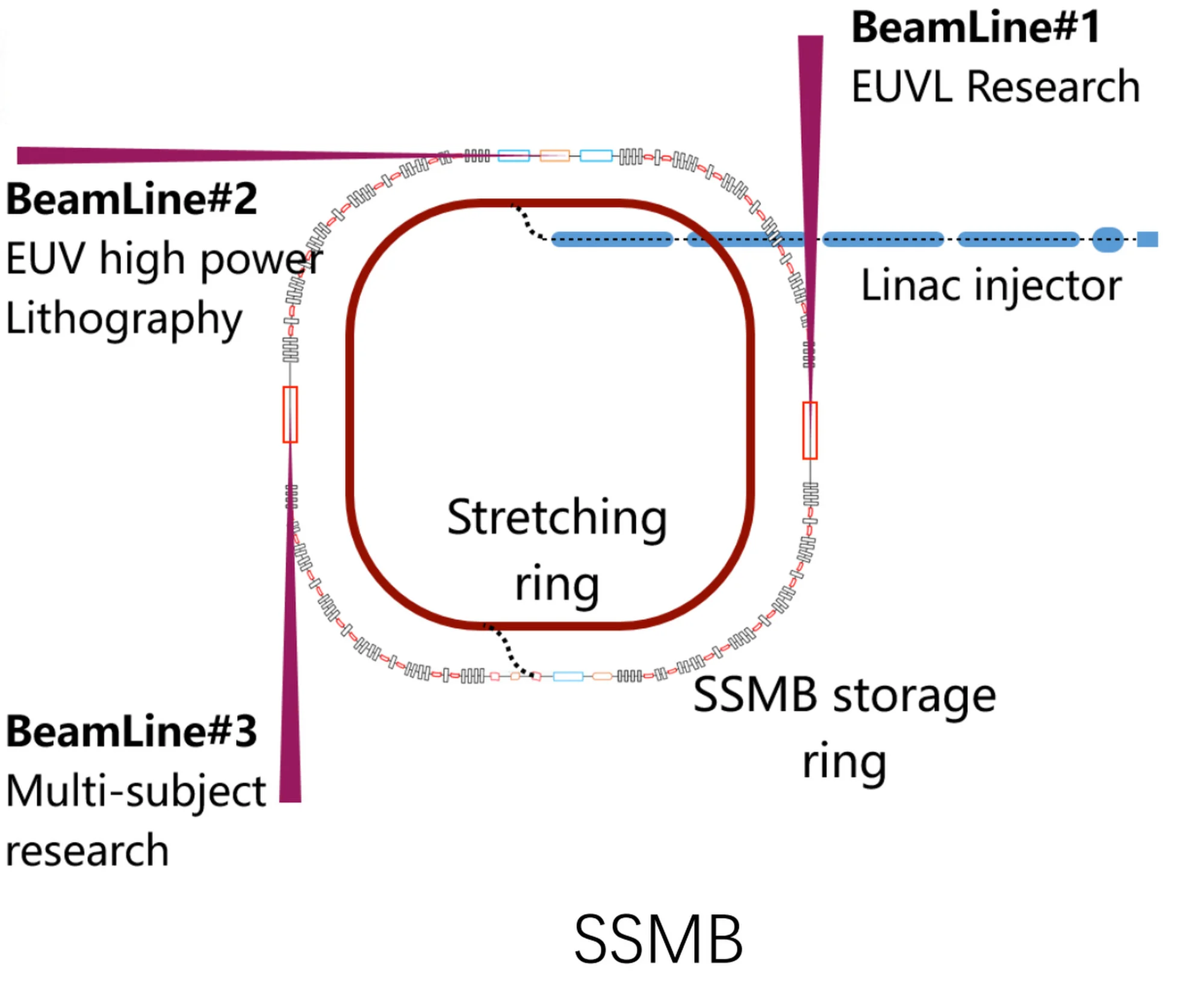
The Chinese research team, led by Tsinghua University, is developing a unique laser source using particle accelerators. Their goal is to sidestep the constraints of conventional lithography machines, which are pivotal in microchip production. The proposed particle accelerator will be roughly the size of two basketball courts, between 100-150 meters in circumference, and will serve as a high-quality light source for chip fabrication.
Professor Zhao Wu from Stanford University introduced the underlying technology, termed steady-state microbunching (SSMB). SSMB captures the energy emitted by charged particles during acceleration, transforming it into a continuous, pure EUV light source. Compared to the prevalent ASML EUV method, SSMB boasts superior power and efficiency, potentially reducing chip production costs.
"An SSMB-EUV light source has been designed at THU, with designed EUV power higher than 1kW, and some key technologies are nearly ready," said team member Professor Pan Zhilong at a presentation at an academic workshop in January 2022.
This ambitious project contrasts with the strategies of companies like ASML, which focus on miniaturizing chip-making machines. Instead, China's vision involves creating a giant factory that houses several lithography machines, all centered around a single accelerator. This design aims to enable competitive manufacturing processes (such as 2nm and beyond) that will be used to make high-performance chips without using traditional extreme ultraviolet (EUV) lithography scanners.
"As a completely new light source, the experimental verification of the technology has been implemented. But it is necessary to build a solid SSMB light source research device operating in the EUV band," said project leader Professor Tang Chuanxiang from Tsinghua University.
"Then we can [use the device to] cultivate scientific and industrial users, and polish the SSMB technology."
Get Tom's Hardware's best news and in-depth reviews, straight to your inbox.
According to the report, Tsinghua University's team has made significant strides in this domain; they have successfully trialed the technology and are now scouting locations for the project's construction, the report claims. Their achievements could pave the way for China to bypass potential future sanctions and emerge as a semiconductor powerhouse.
However, the journey to realizing SSMB-based EUV lithography machines remains long and challenging. Professor Tang Chuanxiang heads the project and emphasizes the need for continuous innovation and collaboration across industries to develop a functional lithography system.
"There is still a long way to go before our independent development of EUV lithography machines, but SSMB-based EUV light sources give us an alternative to the sanctioned technology," said Tang. "It requires continuous technological innovation based on SSMB EUV light sources and cooperation with upstream and downstream industries to build a usable lithography system."

Anton Shilov is a contributing writer at Tom’s Hardware. Over the past couple of decades, he has covered everything from CPUs and GPUs to supercomputers and from modern process technologies and latest fab tools to high-tech industry trends.
-
gg83 Enough of these articles. Please stop copy and posting crud from untrustworthy "news" organizations.Reply -
rluker5 So what would having the laser run around an additional circle have to do with the lithography? Maybe it would be a different way of doing the first part of getting the beam handy, but don't they also do a ton of stuff to get the pattern sized and focused and keep the beam clean?Reply
Seems like a lot of extra work for no good reason. Like if you sold your old GPU on Ebay and shipped it to Indonesia, then Brazil to get some added stickers before it made it's way back to the buyer in the next state over.
I suppose a more apt comparison would be if I found a new light bulb treatment for my video projector that was the size of a bookshelf and tubed that into where the bulb would go in some other brand projector because that new bookshelf bulb would somehow make a better picture? A bookshelf sized bulb contraption doesn't seem like a reinvention of the projector that is doing the light manipulation for the picture. it is ancillary. -
gg83 Reply
Perfect analogy.!rluker5 said:So what would having the laser run around an additional circle have to do with the lithography? Maybe it would be a different way of doing the first part of getting the beam handy, but don't they also do a ton of stuff to get the pattern sized and focused and keep the beam clean?
Seems like a lot of extra work for no good reason. Like if you sold your old GPU on Ebay and shipped it to Indonesia, then Brazil to get some added stickers before it made it's way back to the buyer in the next state over.
I suppose a more apt comparison would be if I found a new light bulb treatment for my video projector that was the size of a bookshelf and tubed that into where the bulb would go in some other brand projector because that new bookshelf bulb would somehow make a better picture? A bookshelf sized bulb contraption doesn't seem like a reinvention of the projector that is doing the light manipulation for the picture. it is ancillary. -
TJ Hooker Reply
The laser (EUV beam) isn't what's circulating in the accelerator. It's a particle accelerator, not a light accelerator (which wouldn't make sense).rluker5 said:So what would having the laser run around an additional circle have to do with the lithography? Maybe it would be a different way of doing the first part of getting the beam handy, but don't they also do a ton of stuff to get the pattern sized and focused and keep the beam clean?
Seems like a lot of extra work for no good reason.
You need a suitable EUV source for EUV lithography. This is not trivial; it took ASML decades to get a working method. A particle accelerator is apparently another method for generating EUV suitable for lithography. They're not just doing it for fun, they're doing it because they can't use the same type of source as others due to sanctions.
It'd be like if you couldn't buy a normal projector bulb, nor could you buy the parts to make a normal bulb yourself. So you come up with a different light source, because otherwise you can't use your projector.rluker5 said:I suppose a more apt comparison would be if I found a new light bulb treatment for my video projector that was the size of a bookshelf and tubed that into where the bulb would go in some other brand projector because that new bookshelf bulb would somehow make a better picture? A bookshelf sized bulb contraption doesn't seem like a reinvention of the projector that is doing the light manipulation for the picture. it is ancillary.
I have no idea how effective this setup with be for generating EUV for lithography. But it seems pretty obvious what they're trying to do and why. -
BFG-9000 Well we could make antimatter in particle accelerators too if we wanted to, for only a NASA estimated cost of $62.5 trillion per gram.Reply
Perhaps they are willing to pay the price to produce a Potemkin village of a phone like the Mate 60 just for bragging rights, but it seems an unlikely method to produce saleable and profitable products.
Hmm, would you rather be able to thumb your nose at sanctions, or produce a photon torpedo? -
TJ Hooker Reply
Antimatter is already being made in particle accelerators, and it didn't cost trillions of dollars. Do you have a source for that estimate? Maybe they were estimating to produce some large amount (e.g. a kg of antimatter).BFG-9000 said:Well we could make antimatter in particle accelerators too if we wanted to, for only a NASA estimated cost of $62.5 trillion per gram.
https://home.cern/science/physics/antimatter -
Darkoverlordofdata And in another article, you state that they have issues raising money for current technology.Reply
Maybe this is more like the Starwars/Strategic Defense Initiative - they are luring US down the same rabbit hole. -
BFG-9000 Reply
So far, CERN has made less than 10 nanograms of antimatter and at that rate (which is ~1 nanogram per year if the accelerators are used to do nothing but produce antimatter) would take 1 billion years to produce 1 gram. Production of antimatter at a reasonable rate using particle accelerators would therefore require covering much of the earth in particle accelerators and the energy infrastructure to power them, hence NASA's estimate of $62.5 trillion per gramTJ Hooker said:Antimatter is already being made in particle accelerators, and it didn't cost trillions of dollars. Do you have a source for that estimate? Maybe they were estimating to produce some large amount (e.g. a kg of antimatter).
https://home.cern/science/physics/antimatter
The efficiency of antimatter production in particle accelerators is so low that about 1 billion times more energy is required to make antimatter than is finally contained in its mass. Using E = mc^2, we find that 1 gram of antimatter contains:
0.001 kg x (300,000,000 m/s)2 = 90,000 GJ = 25 million kWh
Taking into account the low production efficiency, it would need 25 million billion kWh to make one single gram
