Intel Shows New Stacked CFET Transistor Design At ITF World
Twice the nanosheets.
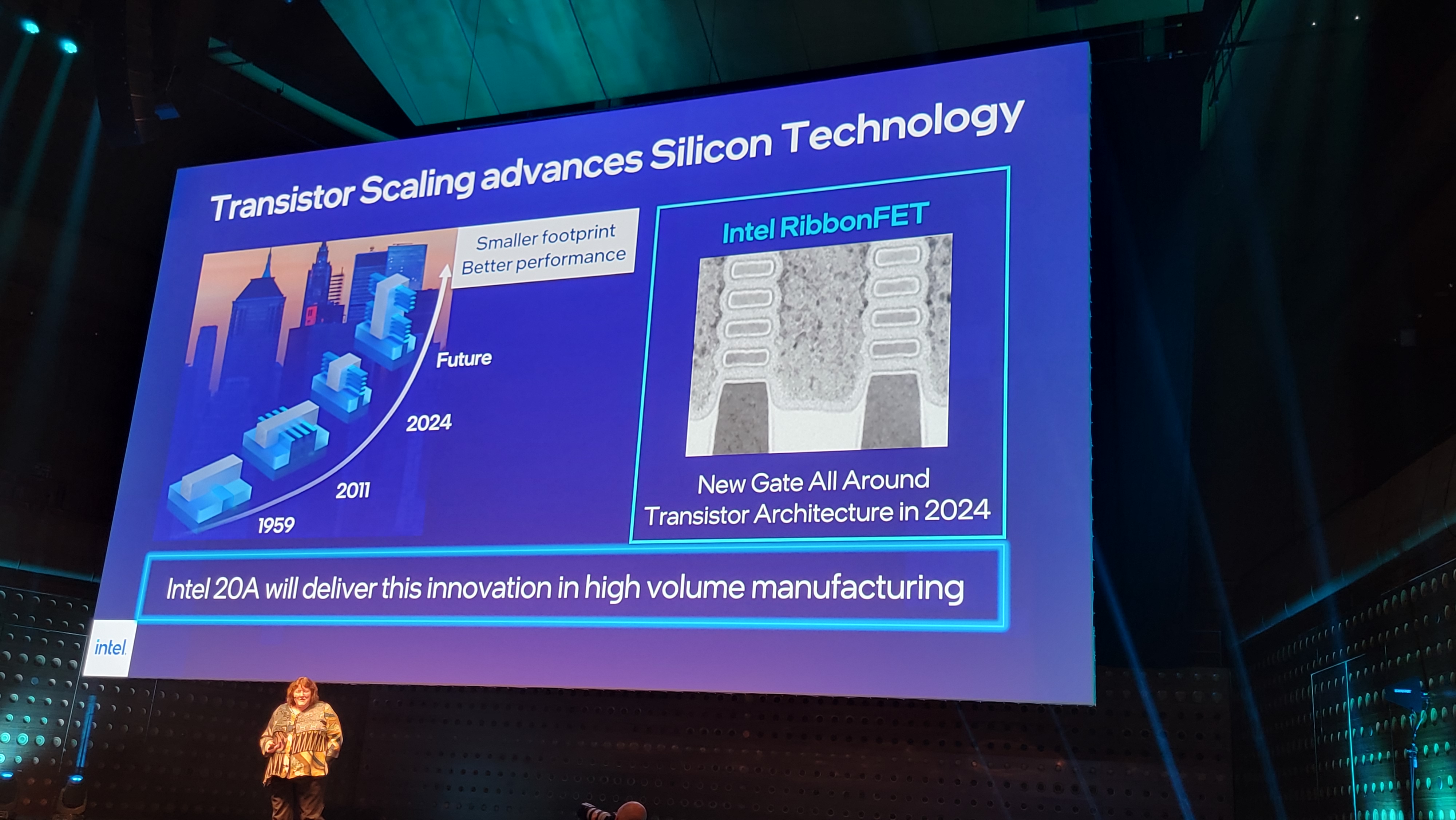
At ITF World 2023 in Antwerp, Beligum, Ann Kelleher, Intel’s Technology Development GM, presented an outline of Intel’s latest developments in several key areas, and one of the most interesting revelations was that Intel would embrace stacked CFET transistors in the future. This marks the first time that Intel has shown this new type of transistor in its presentations, but Kelleher didn’t provide a date or firm timeline for production.
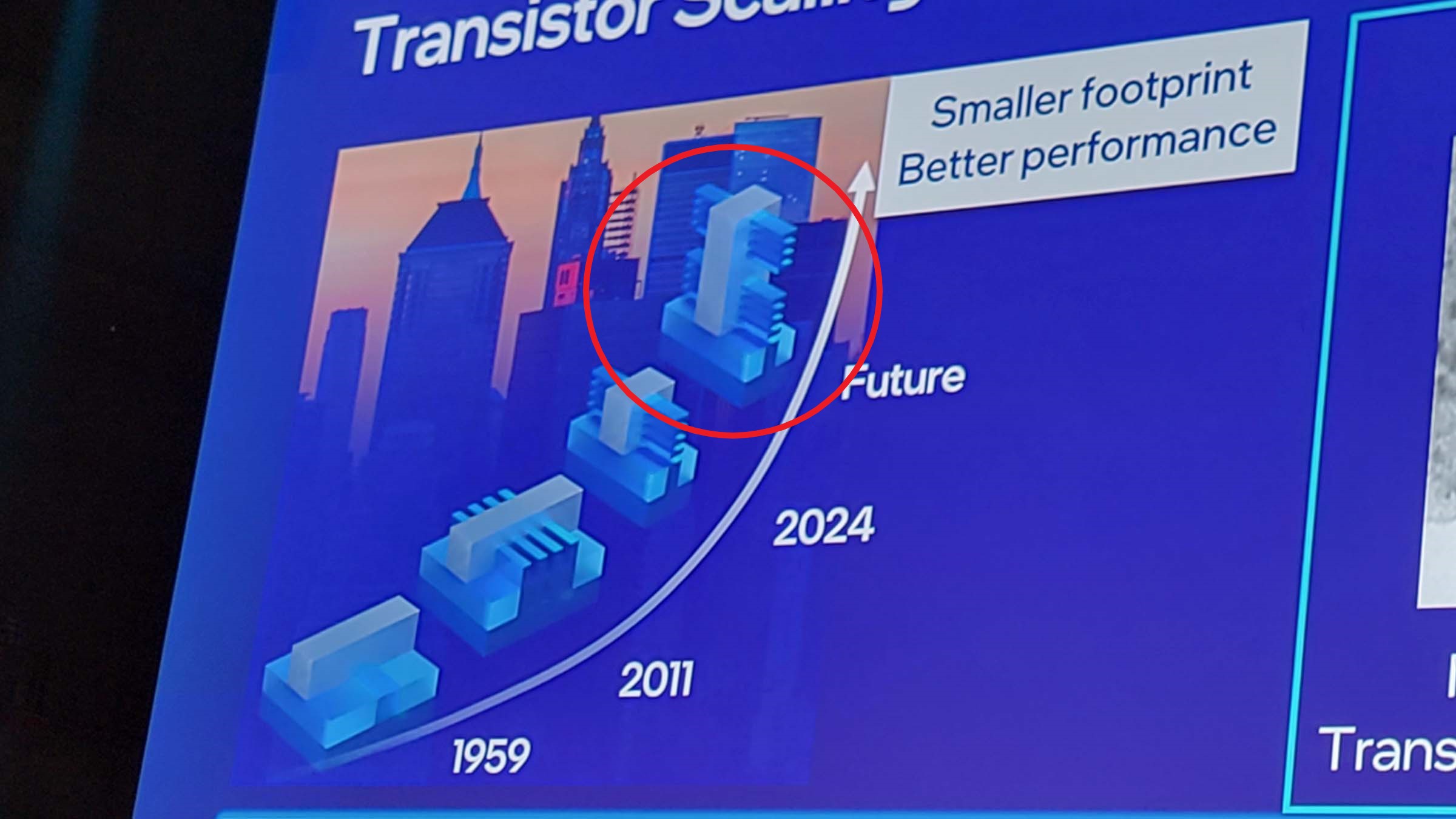
Here we can see a zoomed-in version of the slide with a ring added around the new type of transistor. The first two transistor types at the bottom of the slide are older variants, while the ‘2024’ entry represents Intel’s new RibbonFET transistors that we’ve covered extensively in the past. Intel's first-gen design with the 'Intel 20A' process node features four stacked nanosheets, each surrounded entirely by a gate. Kelleher says this design remains on track to debut in 2024. RibbonFET uses a gate-all-around (GAA) design, which confers both transistor density and performance improvements like faster transistor switching while using the same drive current as multiple fins, but in a smaller area.
Kelleher’s slide also shows the next generation of Intel’s GAA design – the stacked CFET. The Complementary FET (CFET) transistor design has been on imec’s roadmaps for some time, but we haven’t yet heard the company state that it plans to adopt this design. As a reminder, the imec research institute studies future technologies and collaborates with the industry to bring them to fruition.
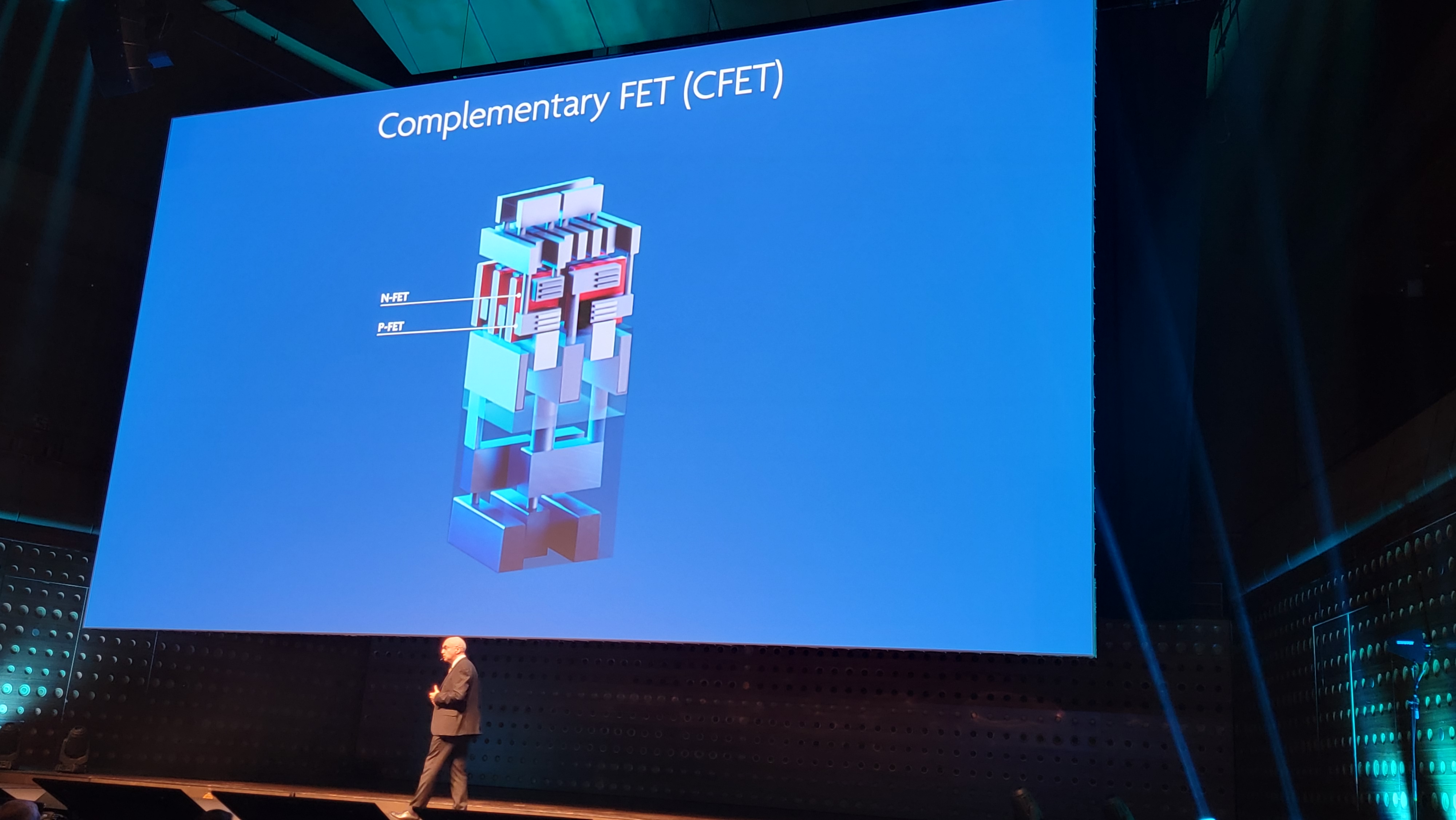
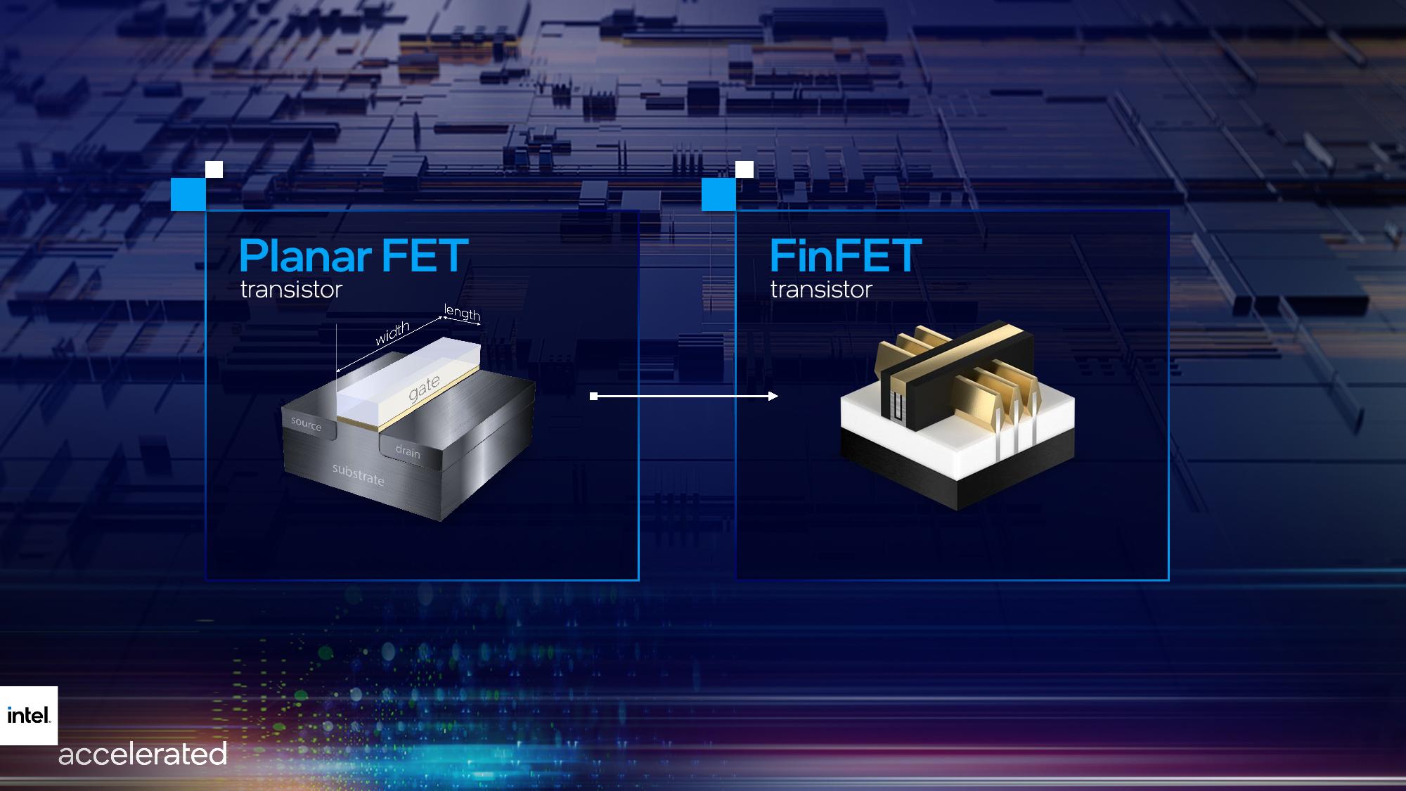

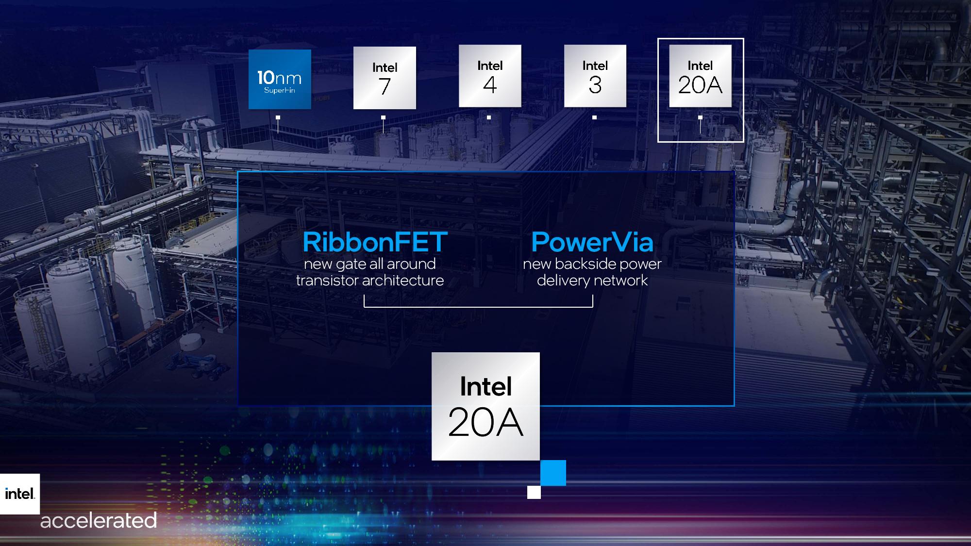
Naturally, there is some variation between Intel’s stylized render and the imec CFET render we’ve included in the first image of the album above, but Intel’s image conveys the point well – this design allows the company to stack eight nanosheets, a doubling of the four used with RibbonFET, thus increasing transistor density. We also have images of the three other types of Intel transistors in the album above — Planar FET, FinFET, and RibbonFET.
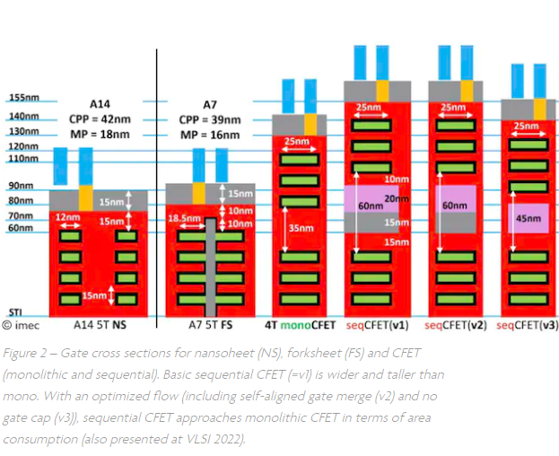
CFET transistors, which you can read more about here, stack n- and pMOS devices atop each other to enable higher density. Two types of CFETs are currently being researched — monolithic and sequential. The four devices on the right side of the above image detail various proposed CFET designs. For now, it is unclear which type of design Intel would adopt, or if it will devise another type of implementation. Given that imec doesn’t have CFETs on its roadmap until around when chips shrink to 5 angstroms in the 2032 timeframe, it could be some time before we find out.
That said, it isn’t guaranteed that Intel would target CFET in that timeframe: Interestingly, Intel’s slide shows its next-gen GAA nanosheet transistor (RibbonFET) and then jumps directly to CFET, omitting the GAA forksheet transistors that most think will be the step between nanosheet and CFET. You can also see that type of transistor in the above slide — it is the second from the left.
Given that Intel’s image isn’t very detailed, it is possible that the company also plans to use forksheet transistors before it moves to CFET, but it hasn’t chosen to share the details yet. We’re following up with Intel to see if we can learn any more details.
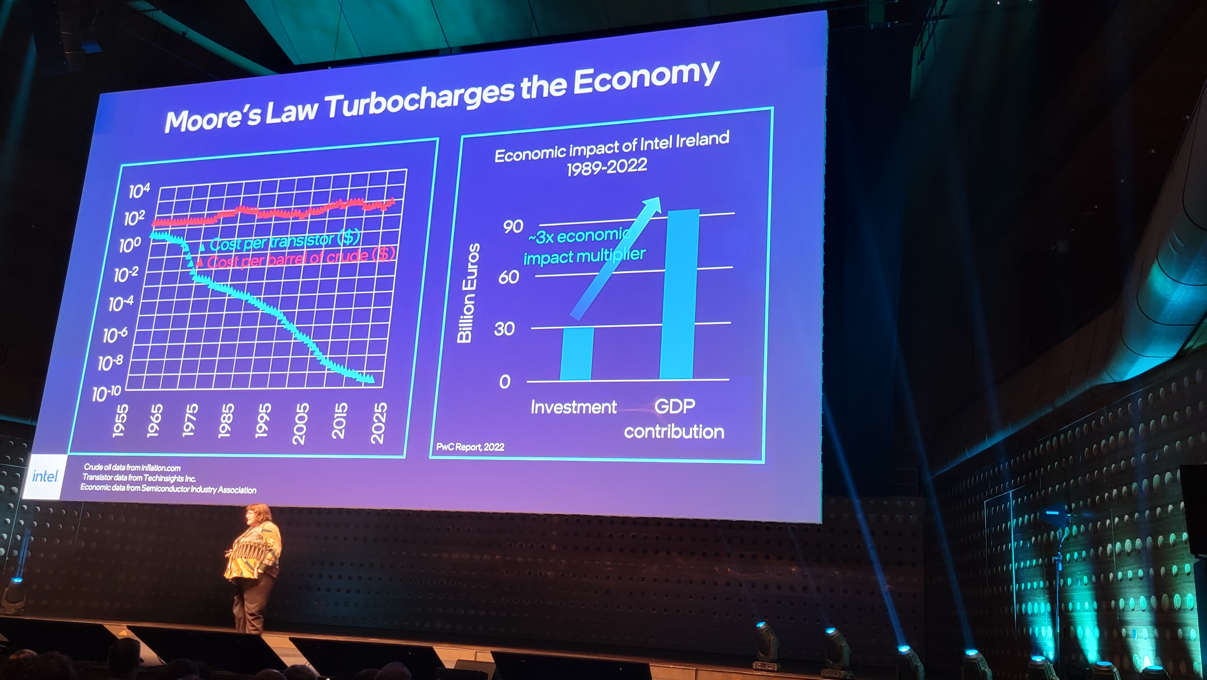
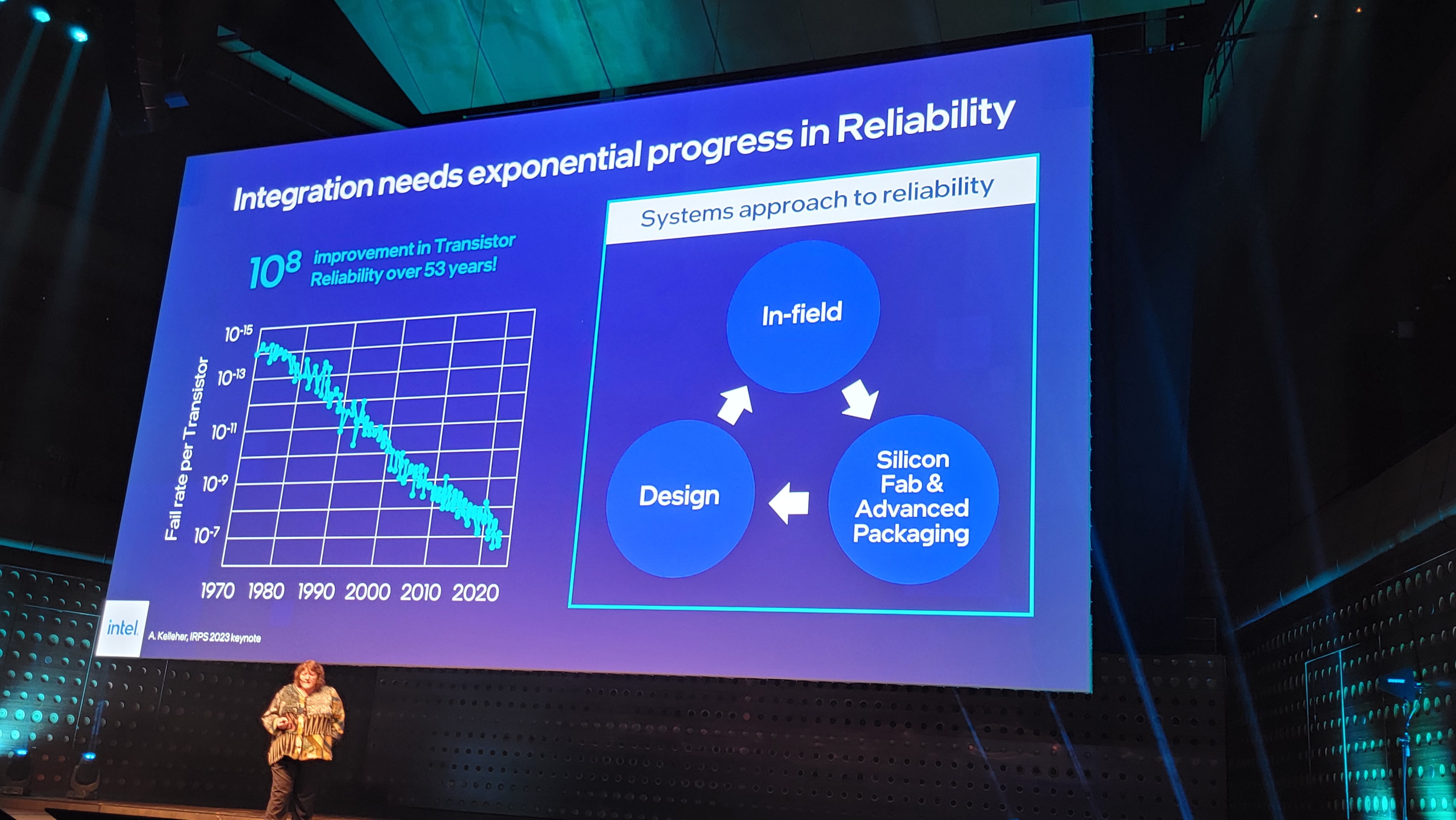
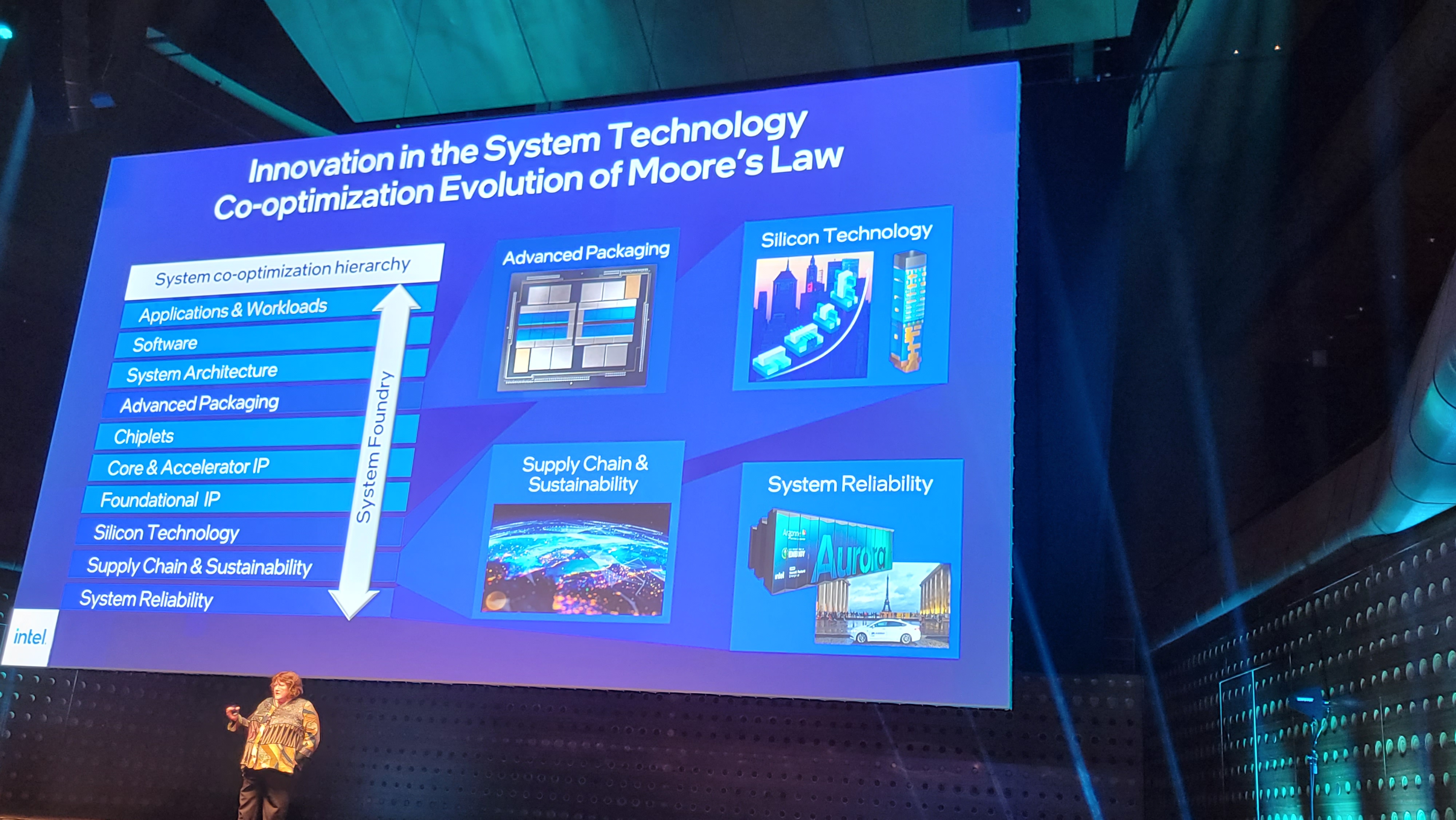

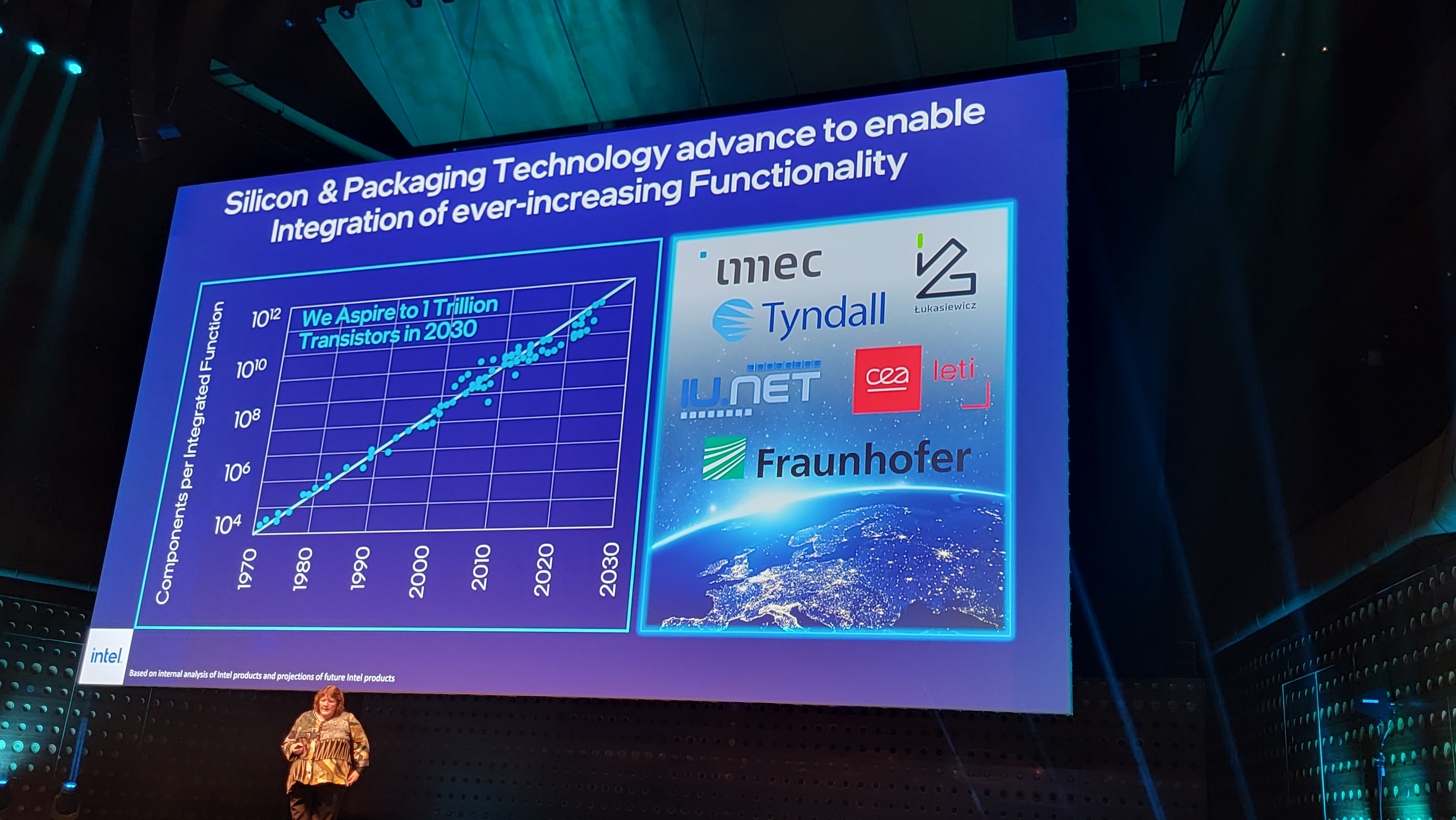


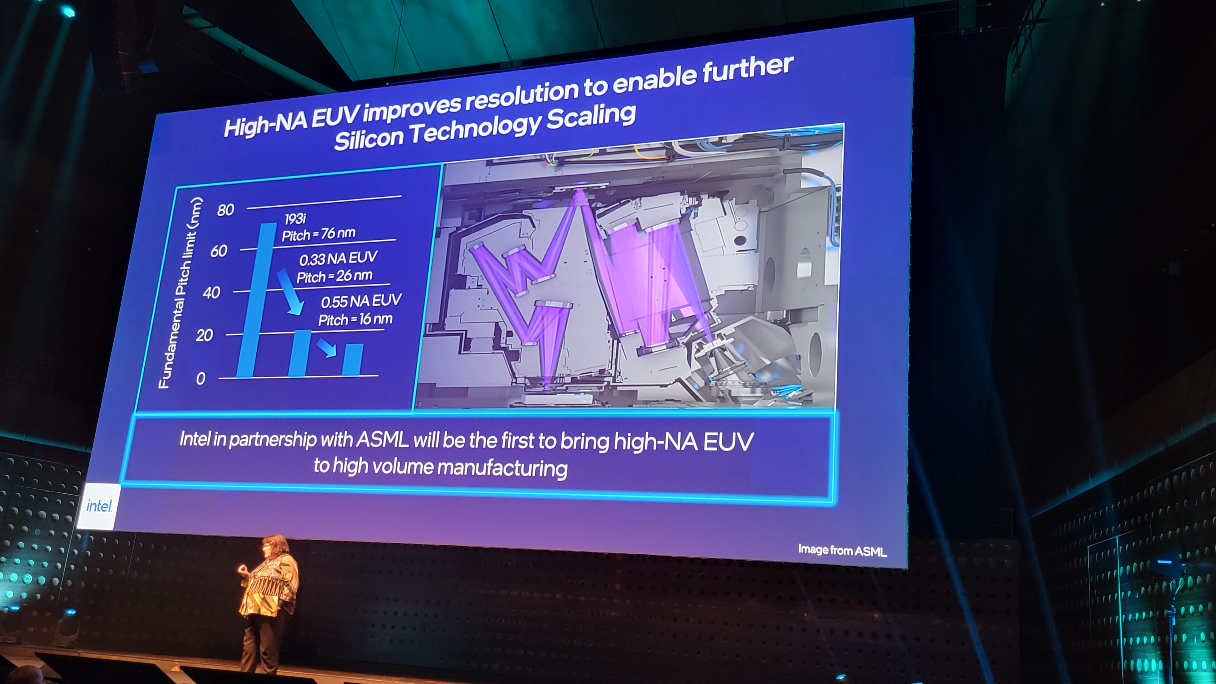
Here are the remainder of the slides from Kelleher’s presentation for your perusal. Kelleher covered a diverse range of topics, including the decline in the cost paid per transistor over time, the increase in the reliability of transistors over time, the increasingly complex packaging process, and the importance of a shift to the System Technology Co-Optimization methodology for Intel's design efforts.
Kelleher’s presentation took place at imec’s ITF World conference, and she opened her speech by reminiscing on her own history with imec – she first worked for imec as a student nearly thirty years ago, eventually spending two years with the research giant. Intel also has a long relationship with imec spanning over the last 30 years, and that work continues today.
You might not be familiar with the Interuniversity Microelectronics Centre (imec), but it ranks among the most important companies in the world. Think of imec as a silicon Switzerland, of sorts. Imec serves as a quiet cornerstone of the industry, bringing fierce rivals like AMD, Intel, Nvidia, TSMC, and Samsung together with chip toolmakers such as ASML and Applied Materials, not to mention the critical semiconductor software design companies (EDA) like Cadence and Synopsys, among others, in a non-competitive environment. This collaboration allows the companies to work together to define the roadmap of the next generation of tools and software they will use to design and manufacture the chips that power the world.
Get Tom's Hardware's best news and in-depth reviews, straight to your inbox.

Paul Alcorn is the Editor-in-Chief for Tom's Hardware US. He also writes news and reviews on CPUs, storage, and enterprise hardware.
-
InvalidError Once you have GAA where the transistor channel isn't tied to the substrate anymore, the only limit to how many transistors you can stack on each other is thermal density. CFET is only the logical first step beyond GAA.Reply -
Paul Alcorn Reply
Most of the industry predicts that forksheets come first, actually.InvalidError said:Once you have GAA where the transistor channel isn't tied to the substrate anymore, the only limit to how many transistors you can stack on each other is thermal density. CFET is only the logical first step beyond GAA. -
InvalidError Reply
Forksheets are nothing more than two GAA stacks sharing a gate drive signal for space efficiency. IMO, this is far too obvious an improvement to call out separately as it makes no sense to build a GAA inverter gate/buffer any other way.PaulAlcorn said:Most of the industry predicts that forksheets come first, actually. -
Paul Alcorn Reply
They're called out in roadmaps separately, as they increase density significantly and will serve for a few years before CFET comes to fore. Bringing nFET and pFET together seems to be a pretty significant and complicated advance to me, as well as the use of the dielectric barrier.InvalidError said:Forksheets are nothing more than two GAA stacks sharing a gate drive signal for space efficiency. IMO, this is far too obvious an improvement to call out separately as it makes no sense to build a GAA inverter gate/buffer any other way. -
InvalidError Reply
The only difficulty in "bringing them together" was that with FinFET, manufacturers were still stuck in 2D for transistor construction. With GAA eliminating this restriction, almost any transistor configuration is possible now. It doesn't need to stop at stacking only one p-n pair, you could build many 2-3 inputs logic functions vertically depending on how many active layers you are willing to stack.PaulAlcorn said:Bringing nFET and pFET together seems to be a pretty significant and complicated advance to me, as well as the use of the dielectric barrier.
The only thing that makes forked "easier" is that it requires half as many total layers vs stacked CMOS pairs but it also has only about half as much areal density.
As I have written before, the main problem is power density: if you stack transistors N-high, you need to find a way to deal with having up to N-times that much power density.
We know from NAND that layers are at least 20X cheaper than die area. Now that the vertical genie for high-speed CMOS is out of the bottle, stacked transistors are inevitable. -
Arbie I used to believe what Intel said; and excited to watch it come true. Those were the days.Reply -
MattTraversoPhD Reply
There are other major limitations to stacking more than 2 layers in CFET, specifically routing. Each transistor needs 3 contacts (source, drain, gate) and sometimes transistors can share multiple. CFET works because most transistors in CMOS architecture are paired so they can share contacts (usually the source and the gate). If you start adding 3 or 4 transistors in a stack, you quickly run out of surface area for all the contacts to connect to all the transistors in a stack. When transistors in a stack aren't paired, it also becomes challenging (but surmountable) to vertically isolate their gates from each other.InvalidError said:The only difficulty in "bringing them together" was that with FinFET, manufacturers were still stuck in 2D for transistor construction. With GAA eliminating this restriction, almost any transistor configuration is possible now. It doesn't need to stop at stacking only one p-n pair, you could build many 2-3 inputs logic functions vertically depending on how many active layers you are willing to stack.
The only thing that makes forked "easier" is that it requires half as many total layers vs stacked CMOS pairs but it also has only about half as much areal density.
As I have written before, the main problem is power density: if you stack transistors N-high, you need to find a way to deal with having up to N-times that much power density.
We know from NAND that layers are at least 20X cheaper than die area. Now that the vertical genie for high-speed CMOS is out of the bottle, stacked transistors are inevitable.
3DNAND is a special case because little routing is needed. Each stack shares 1 source and 1 drain and the gates are shared by thousands of transistors in a plane, each. Even still, the staircase structures needed to contact each NAND gate are complex and non-trivial to manufacture.
Mono CFET also presents challenges to create the nanosheets and then etch deep enough that will probably limit the number of ribbons in a stack for a while. Sequential CFET with several layers of interconnects between the ribbons would be a possibility for solving both the routing problems and the stack pattern problems, but at that point, you're looking at something more in common with Foveros/active interposer than a monolithic chip solution.
Bottom line, although possible, I don't see it very likely to move beyond a stack of 2 paired transistors of CFET quickly.
I agree with your assessment of Forksheet. It's basically GAAFET with a dielectric to split each fin in half so that both PMOS and NMOS operate on the same fin.
I'm a former technical trainer in semiconductor manufacturing. I trained new hires on process flow and capabilities. I've been writing articles on medium about finfet, gaafet and cfet for a more general audience. I won't link them, here, but you can look me up. -
InvalidError Reply
I don't see how vertical gate isolation would be any more difficult than the N-channel and P-channel ribbon isolation when gates have always been vertically isolated from everything else in planar FETs - just don't etch a hole in the silicon oxide layer between layers that aren't supposed to connect to each other.MattTraversoPhD said:There are other major limitations to stacking more than 2 layers in CFET, specifically routing. Each transistor needs 3 contacts (source, drain, gate) and sometimes transistors can share multiple. CFET works because most transistors in CMOS architecture are paired so they can share contacts (usually the source and the gate). If you start adding 3 or 4 transistors in a stack, you quickly run out of surface area for all the contacts to connect to all the transistors in a stack. When transistors in a stack aren't paired, it also becomes challenging (but surmountable) to vertically isolate their gates from each other.
As for sharing contacts, one stage's output is the next stages' input. Full adders and things like XOR would benefit quite a bit from going 4-high where stages could be cascaded using little more than vias. -
JayNor Intel presented on 2d materials at IEDM in Dec. Any new info presented on 2d materials?Reply -
Diogene7 ReplyMattTraversoPhD said:There are other major limitations to stacking more than 2 layers in CFET, specifically routing. Each transistor needs 3 contacts (source, drain, gate) and sometimes transistors can share multiple. CFET works because most transistors in CMOS architecture are paired so they can share contacts (usually the source and the gate). If you start adding 3 or 4 transistors in a stack, you quickly run out of surface area for all the contacts to connect to all the transistors in a stack. When transistors in a stack aren't paired, it also becomes challenging (but surmountable) to vertically isolate their gates from each other.
3DNAND is a special case because little routing is needed. Each stack shares 1 source and 1 drain and the gates are shared by thousands of transistors in a plane, each. Even still, the staircase structures needed to contact each NAND gate are complex and non-trivial to manufacture.
Mono CFET also presents challenges to create the nanosheets and then etch deep enough that will probably limit the number of ribbons in a stack for a while. Sequential CFET with several layers of interconnects between the ribbons would be a possibility for solving both the routing problems and the stack pattern problems, but at that point, you're looking at something more in common with Foveros/active interposer than a monolithic chip solution.
Bottom line, although possible, I don't see it very likely to move beyond a stack of 2 paired transistors of CFET quickly.
I agree with your assessment of Forksheet. It's basically GAAFET with a dielectric to split each fin in half so that both PMOS and NMOS operate on the same fin.
I'm a former technical trainer in semiconductor manufacturing. I trained new hires on process flow and capabilities. I've been writing articles on medium about finfet, gaafet and cfet for a more general audience. I won't link them, here, but you can look me up.
I don’t really understand why so much exponential technical and financial resources are allocated to attempt to maybe gain low performance and low power efficiency incremental improvements (10% / 15%) on a technology, like silicon transistors, that is close to reaching its limit and is a dead end, versus re-allocating those resources to significantly invest in next generation computing technologies like spintronics related technologies (MRAM, Intel MESO concept, French R&D Spintec FESO concept,…) as it seems that could improve power efficiency from 5x to 30x with plenty new opportunities (better suited for AI,…) which, at this point (2023) seems quite obviously (to myself at least) the next step.
The development of CFET is much too expensive compared to the opportunities that spintronic related technologies would provide : CFET is unfortunately delaying a much better technology (spintronic technologies).
Also I don’t understand that at this stage DARPA and the US government (US CHIPS Act) still don’t yet make it a top priority fin order that the US regain its technological leadership…