Imec, the most advanced semiconductor research firm in the world, recently shared its sub-'1nm' silicon and transistor roadmap at its Future Summit event in Antwerp, Belgium. The roadmap gives us a rough idea of the timelines through 2036 for the next major process nodes and transistor architectures the company will research and develop in its labs in cooperation with industry giants, like TSMC, Intel, Samsung, and ASML, among many others.
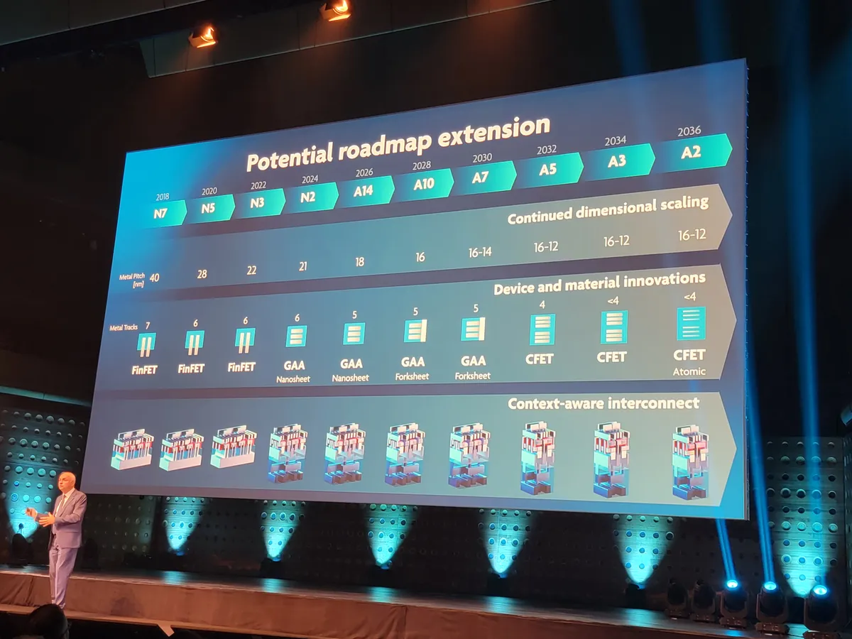
The roadmap includes breakthrough transistor designs that evolve from the standard FinFET transistors that will last until 3nm, to new Gate All Around (GAA) nanosheets and forksheet designs at 2nm and A7 (seven angstroms), respectively, followed by breakthrough designs like CFETs and atomic channels at A5 and A2. As a reminder, ten Angstroms are equal to 1nm, so Imec's roadmap encompasses sub-'1nm' process nodes.
You might not have heard of the Interuniversity Microelectronics Centre (imec) before, but it ranks among the most important companies in the world, alongside better-known companies like TSMC and EUV-toolmaker ASML. Think of imec as a silicon Switzerland, of sorts. While the semiconductor research-focused imec doesn’t operate with much fanfare, it serves as the quiet cornerstone of the semiconductor industry, bringing fierce rivals like Intel, TSMC, and Samsung together with chip toolmakers such as ASML and Applied Materials, not to mention the equally-critical semiconductor software design companies (EDA) like Cadence and Synopsys, in a non-competitive environment. This collaboration allows the companies to work together to define the next generation of tools and software they will use to design and manufacture the chips that power the world.
A standardized approach is becoming increasingly important in the face of the profoundly increasing complexity and cost of designing the chips, and the tools that make them. Imec also partners with customers, like Intel or TSMC, among many others, for R&D on new technologies they can use in their latest processors. The company is also famous for helping pioneer EUV technology in concert with its long-time partner ASML.
At the end of the day, all of the leading-edge chipmakers use much of the same equipment sourced from a few critical toolmakers, so some level of standardization is necessary. However, that requires R&D efforts that can begin a decade before deployment, meaning that imec’s roadmaps can give us a much longer view of the upcoming advances in the semiconductor industry than the nearer-term product roadmaps from companies like AMD, Intel, and Nvidia. In fact, many of those products wouldn’t even be possible without the collaborative work undertaken years in advance at imec. Let's take a closer look at the roadmap and some of the complementary tech behind it.
Defining the Problem


The industry faces increasing challenges as nodes progress, costs skyrocket, and the demand for more computing power, particularly for machine learning, increases non-linearly.
Imec is fully convinced that Moore’s Law is still alive and well 52 years after it was penned, though we think that doesn't apply to the economic component of the law that also defined a lower cost per transistor over time. In fact, as shown above, chip design costs are skyrocketing due to more complex design rules and longer design cycle times, contributing to increased cost-per-transistor. Additionally, single-threaded performance gains are slowing from the heady days of 50% yearly gains in the late 90s and early 2000s to ~5% per year.
However, if we don't take density or economics into account, Moore’s Law generally remains on track with doubled transistor counts every two years — Apple’s M1 Ultra with 114 billion transistors even exceeds that watermark. To combat the declining gains in single-threaded performance, we've seen the rise of domain-specific compute devices (specialized processors designed for a narrow set of tasks) like GPUs. These devices are normally heavily parallelized, thus allowing power/performance and area efficiency to improve at a more rapid rate.
Imec points out that while the need for more compute power used to double every two years, basically in line with the performance increases provided by adherence to Moore's Law, the raw compute power needed for machine learning/AI doubles approximately every six months. That presents a vexing problem, as even a continued doubling of transistor counts won't be able to keep pace. Imec thinks a three-pronged solution of dimensional scaling (including better density and packaging tech), new materials and device architectures, and system technology co-optimization (SCTO) can keep the industry on track.
Imec's Transistor and Sub-1nm Process Node Roadmap


The first step is to enable the next-gen tools. Today's 4th-Gen EUV lithography machines have a 0.33 aperture, so chipmakers will have to use multi-patterning techniques (more than one exposure per layer) to create the smallest of features at 2nm and beyond. Because the wafer will have to be 'printed' twice for a single layer, there's a higher chance of defects. That will result in reduced yields and longer cycle (production) times, contributing to increased costs.
The next-gen High-NA models (5th-Gen) will have a 0.55 aperture. This higher level of precision will allow the creation of even smaller structures in a single exposure, thus reducing design complexity and improving yields, cycle times (200+ wafers per hour), and cost. Imec and ASML expect these tools to be available for mass production in the 2026 timeframe. The first $400 million High NA tool will be completed at ASML in the first half of 2023. Imec will operate at the test lab at the ASML facility to speed access to the machine for chipmakers, a first (ASML usually ships the tool to imec's fab).
Intel will be the first company to receive a High NA EUV tool, the Twinscan EXE:5200, officially slated for delivery in 2025.
The second slide in the above album shows the roadmap for new types of transistors that will enable further density scaling and hopefully some performance improvement, too. Gate All Around (GAA)/Nanosheet transistors debut in 2024 with the 2nm node, replacing the FinFETs that power today's leading-edge chips. We've already seen announcements from several chipmakers, like Intel's quad-sheet RibbonFET, that incorporate different variations of this transistor technology.
As a reminder, ten Angstroms (A) equal one 1nm. That means A14 is 1.4nm, A10 is 1nm, and we go to the sub-1nm era in the 2030 timeframe with A7. However, the process naming node convention has turned into more of a marketing exercise for the chipmarkers rather than a metric tied to any sort of physical measurement. In the real world, a plethora of factors influences the economics and performance of a process node, such as transistor density, peak performance, performance per watt, different types of logic/circuits, SRAM density, and so on. In its charts, imec uses the metal and poly pitch in tandem with the standard naming conventions to provide a few other important metrics. We can also see transistor density measurements in ASML's slide (second from the last in the above album).
Imec expects GAA/nanosheet and forksheet transistors (at its most basic level, a denser version of GAA) to last through the A7 node. Complementary FET (CFET) will transistors will shrink the footprint even further when they arrive around 2032, allowing more densely-packed standard cell libraries. Eventually, we'll see versions of CFET with atomic channels, which will further improve performance and scalability.
As you can see in the last two slides (presented by ASML at the event), standard DUV brought us to 100 MTr/mm^2 (mega-transistor per squared millimeter, a density measurement), while today's 0.33NA will propel the industry to ~500 MTr/mm^2. The coming High NA machines will be needed at 2nm to bring that up to ~1000 MTr/mm^2, and perhaps beyond with multi-patterning.
Imec's BEOL 'Scaling Boosters' Roadmap


Further increasing transistor density and performance characteristics will also require enhanced Back End of Line (BEOL) processes. The BEOL steps focus on wiring the transistors together, enabling both communication (signals) and power delivery.
Imec calls these secondary density-improving techniques 'scaling boosters,' as they contribute to increased transistor density and performance even though they aren't directly related to the size/placement of the transistors.
Backside power distribution is a key advancement that brings power to the backside of the chip, with Intel already announcing its own version of this technique, dubbed PowerVIA. This technique routes all power for the transistors directly to the transistors through the backside of the transistor, partitioning power delivery to the backside of the transistors while data transmission interconnects remain in their traditional location on the other side.
Separating the power circuitry and the data-carrying interconnects improves voltage droop characteristics, allowing for faster transistor switching while enabling denser signal routing on the top of the chip. Signaling also benefits because the simplified routing enables faster wires with reduced resistance and capacitance. Imec firmly believes that backside power delivery will extend to all leading-edge chips and has been working on this technology for five years, creating its own unique patented backside power delivery technology.
Naturally, heat could become an issue with backside power delivery as the transistors will have metal layers placed on the side of the silicon that usually dissipates heat. Still, imec tells us that the metals used (currently copper) are adept enough at dissipating heat to reduce the impact. However, some design considerations will need to be made to accommodate this technique.
Further improvements on the roadmap include direct metal etch techniques for interconnects, along with self-aligned vias with air gaps. Interconnects, the tiny wires that enable power delivery and communication, have become one of the biggest barriers to scaling. That problem is becoming more pronounced over time — the width of these wires will need to be only a few atoms thick. Imec is also researching new metals that will replace copper, with graphene being among the candidates.
Imec is also researching system technology co-optimization (SCTO) techniques, such as 3D interconnects and 2.5D chiplet implementations. A dearth of Electronic Design Automation (EDA) software for 3D chip designs is the primary inhibitor to wider industry adoption. Imec is working with Cadence to enable advanced software that will simplify the 3D design process.
Stretching out to an even broader view beyond 2030, we see that imec envisions that new materials will replace silicon and the emergence of 2D atomic channels. Imec also believes that magnetics-based gates could emerge as an alternative as the industry inexorably moves towards quantum computing.
