


Intel CEO Pat Gelsinger whipped the covers off the company's new process and packaging roadmap that now stretches out to 2025, outlining an annual cadence of the company's future process nodes spanning from standard nanometer-scale tech down to incredibly small angstrom-class transistors. Intel also teased the first details of its angstrom-class (the next measurement below nanometer) technology, like RibbonFET, its first new transistor design since FinFET arrived a decade ago, and PowerVia, a new backside power delivery technique that sandwiches the transistors between layers of wiring. Intel will also change its process node naming scheme again, this time to match the naming used by external foundries like TSMC. That re-branding begins with Intel's 10nm Enhanced SuperFin, which will now be renamed to 'Intel 7.'
Intel says its process tech will match the current industry leader, TSMC, by 2024, and that it will retake 'process performance leadership' by 2025, helped along by being the first company to receive a next-gen High NA EUV machine from ASML for its next-gen chips. Intel also shared details of its future Foveros Omni and Direct technologies during its 'Intel Accelerated' webcast and announced that its Sapphire Rapids chips would be the "first dual-reticle-sized device" in the industry.
Intel's fledging foundry services business also notched two big wins, with AWS announcing that it will use Intel's packaging services while Qualcomm announced that it will explore using Intel's 20A process for future chip designs. Let's dive in.


Intel Renames 10nm to 7nm
Before we get to the roadmaps, in a necessary move that will likely draw criticism, Intel is renaming its process nodes to align with the current naming conventions used by the third-party foundries like TSMC and Samsung.
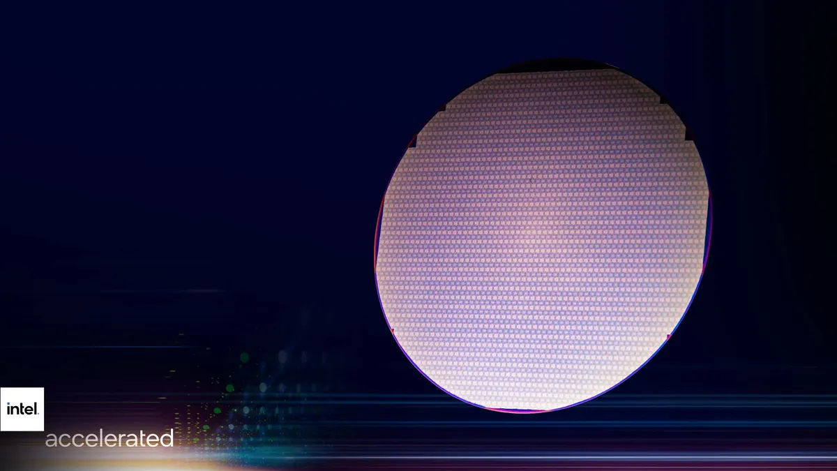
This new policy begins with what was known as the 10nm Enhanced SuperFin process that is set to debut with the Alder Lake processors. Intel announced this process node long ago, and it is already in volume production.
Intel is rebranding the next 10nm node to 'Intel 7' and discarding the 'nanometer' nomenclature, so we won't see the traditional 'nm' suffix attached to the company's process nodes anymore. Instead, Intel will name its nodes based on performance, power, and area advances. As a result, all of Intel's successive node names will be adjusted as well, with Intel's 7nm becoming 'Intel 4,' and so on.
Intel's shift in node naming comes as it builds out its own Intel Foundry Services (IFS) business, which will see it make chips for other companies as part of its IDM 2.0 initiative. Intel's IFS will compete directly with TSMC and Samsung, and given that the node naming convention is already broken, aligning with the rest of the industry makes plenty of sense.
However, changing the 10nm Enhanced SuperFin naming while the 'vanilla' 10nm SuperFin is already shipping definitely isn't as ideal as waiting for an entirely new node to make the change — this approach is unquestionably more confusing. In either case, Intel will eventually have to take criticism for making a change to its nomenclature at some point, and it has chosen to do so with its next line of chips. We'll come back to expand on this topic a bit later in the article.
Intel Process Roadmap 2021 - 2025
Intel's roadmap below starts with the 10nm SuperFin that currently ships in some of its products, like its Tiger Lake processors. However, as noted above, 'Intel 7' is the same 10nm Enhanced SuperFin process that Intel has already announced will power its Alder Lake and Sapphire Rapids chips — it just has a new name.
Similarly, Intel's 7nm, which it recently announced will be delayed, is now branded as 'Intel 4.' The remaining two entries on the roadmap, 'Intel 3' and 'Intel 20A' represent what intel previously branded as 7+ and 5nm, respectively.


Intel says that 'Intel 7,' the process formerly known as '10nm Enhanced SuperFin,' will ship this year for client (Alder Lake), and for the data center (Sapphire Rapids) in the first quarter of 2022. Intel says that 'Intel 7' delivers 10% to 15% more performance-per-watt than its predecessor, 10nm SuperFin.
As normal, that can translate to either higher peak performance (at the expense of efficiency) or increased efficiency (at the expense of performance), but you can't have both simultaneously. It's noteworthy that higher performance doesn't scale linearly due to the increased power required at the upper end of the voltage/frequency curve, so Intel 7 likely won't be 15% faster than 10nm SuperFin.
Moving on to newer climes, Intel 4 (previously known as 7nm) comes to market in products in the first half of 2023, though it will "be ready for production" in the second half of 2022. Intel says this node provides a 20% performance-per-watt gain over its predecessor (the same rules above apply) and represents the company's full embrace of EUV technology. That's an important step forward — Intel's laggardly adoption of EUV fabrication is thought to be a major contributing factor to its 10nm delays.
Chips based on the Intel 4 process will debut in 2023, with client Meteor Lake processors coming in the first half and Granite Rapids server products following. That timeline still leaves Intel's competitors, like TSMC and Samsung, with a process node advantage in the 2023 time frame. TSMC projects it will be in full production of its 3nm node in 2023, explaining Intel's continued need to outsource some products. Intel plans to leverage its packaging technology and disaggregated design philosophy to integrate externally-produced TSMC chips into its own products to help sidestep the delay.
Intel 3, previously branded as 7+, will bring an 18% performance-per-watt gain over Intel 4 when it shows up in products in the second half of 2023. 'Intel 3' is an incredibly fast follow to 'Intel 4' that launches earlier the same year, due to the previously mentioned delays. Still, Intel has confirmed that, based on its early modeling and test chip data, it represents "a higher level of improvement than a standard full node for Intel — or indeed for other vendors."
Intel plans to begin an entirely new era in the first half of 2024: The angstrom era. These chips represent the point where some physical features can no longer be accurately measured in nanometers, or billionths of a meter. Instead, these features will now be measured in angstroms, or one ten-billionth of a meter. The first angstrom-class process from Intel will come as 20A (A is for angstrom), which brings RibbonFET, Intel's first gate-all-around (GAA) transistor, and PowerVia, a novel approach to delivering power to incredibly small transistors.
Intel Angstroms, RibbonFET and PowerVia


RibbonFET will mark Intel's first gate-all-around (GAA) design and the company's first new transistor design since FinFET debuted in 2011. Intel's design features four stacked nanosheets, each surrounded entirely by a gate. Intel claims this design enables faster transistor switching while using the same drive current as multiple fins, but in a smaller area. This certainly seems plausible; Intel's competitors have also adopted GAA designs.
Intel isn't sharing much information about RibbonFET yet, but it bears a striking resemblance to IBM's recently announced GAA/nanosheet tech that it fabbed on a 2nm test wafer (images below). This is incredibly relevant, as Intel recently announced in its IDM 2.0 announcement that it would collaborate with IBM on future logic and packaging technologies. This partnership is important for Intel as it looks to recover from years of stagnation with its process technologies. During our briefings with IBM about its research results, the company was quite clear that its new 2nm tech will benefit all of its partners, including Intel. You can read more about IBM's similar tech here.

As we noted in our coverage of IBM's nanosheet/GAA tech, the smallest transistors in the world are of no use if you can't wire them together, and that has been one of the most pressing constraints to shrinking to smaller nodes.
Intel's new PowerVia technology seems to be a promising approach to navigating the problem with interconnects. PowerVia routes all power for the transistors directly to the transistors through the backside of the transistor. This essentially partitions power delivery to the backside of the transistors while data transmission interconnects remain in their traditional location on the other side.
Intel says that separating the power circuitry and the data-carrying interconnects improves voltage droop characteristics, allowing for faster transistor switching while enabling denser signal routing on the top of the chip. Signaling also benefits because the simplified routing enables the use of faster wires with reduced resistance and capacitance.
This technique will obviously pose many of its own challenges, such as the power delivery circuitry potentially serving as an insulating layer that traps heat within the transistors. It will be interesting to see how Intel tackles those potential pitfalls.
Intel 18A and High NA EUV

Intel didn't include it in the roadmap, but it already has its next-gen angstrom-class process in development. 'Intel 18A' is already planned for "early 2025" with enhancements to the RibbonFET transistors.
Intel's 18A will be the inflection point for using High NA EUV, which is a new ultra-precise version of EUV machines that can etch designs at smaller (<8nm) resolutions than current machines. These machines will be required to do single-patterning EUV at such fine geometries, while existing EUV tools would require less-desirable multi-patterning EUV techniques.
Intel says it will be the first company to receive a High NA EUV machine from ASML, signaling that it plans to lead with the next-gen EUV machines as opposed to lagging behind TSMC as it did with 10nm. It's noteworthy that while Intel did state that it would be first to receive a High NA EUV machine, it didn't claim that it would be the first to enter high volume manufacturing with High NA EUV.
Intel tells us that it will offer the leading-edge Intel 3 and the following nodes, including 20A and 18A, to its foundry customers. That means we will likely see Intel stick with offering its prospective foundry customers trailing edge nodes for now — Intel 3 doesn't enter production until the second half of 2023.

Intel's summary says that the company will achieve process performance parity with the industry leader, TSMC, in 2024, and take the lead in 2025. However, Intel's footnote specifies that this is based on performance-per-watt, and not transistor performance or density.
It's noteworthy this parity statement only applies to Intel's process tech, and not its end products. The company still plans to still compete with "leadership products" from now until 2025 through a combination of new microarchitectures, packaging innovations that tie together various technologies in new and more efficient ways (more on that below), and also by outsourcing some of its highest-end chip designs for the first time in its history. Intel says it will release both consumer and data center "CPU leadership" chips with an as-yet unspecified TSMC node in 2023.
Intel Packaging Update


Intel's packaging update was a bit more spartan. The company announced that it would use EMIB packaging tech, which uses an embedded silicon bridge in a package to connect multiple dies, for its Sapphire Rapids processors, marking the first data center product with the interconnect technology. This has been a bit of an open secret, as pictures of Sapphire Rapids have already surfaced. However, Intel did reveal that it will improve next-gen EMIB from a 55-micron bump pitch to 45 microns.
Intel's Foveros 3D chip stacking technology debuted in the company's Lakefield processors that the company recently retired, but the next-gen Foveros implementation debuts in Intel's upcoming Meteor Lake processors. This generation of Foveros improves to a 36-micron bump pitch.
Intel's upcoming Foveros Omni takes things a step further. This interconnect technology uses copper columns at the peripheries of the interconnected dies to deliver power, while TSV connections throughout the center of the die shuffle data between the chips. This differs from the first-gen Foveros because it separates the data and power transmission, allowing for cleaner routing for both power and data signals. In turn, this enables a tighter 25-micron bump pitch and allows mixing and matching different base dies. This technology is essentially the same as Intel's ODI packaging tech, which you can read more about here.
Intel has also given its hybrid bonding tech a new use in conjunction with its Foveros packaging. Foveros Direct leverages die-on-wafer hybrid bonding (copper-to-copper) as an alternative to standard thermo-compression bonding. This new technique features aggressive sub-10nm bump pitches that increase interconnect density, simplify interconnect circuitry, and lower resistance and power consumption — all while serving up higher bandwidth. Intel has already taped out a stacked SRAM chip with hybrid bonding, and now the company is applying the technique to its Foveros interconnect. However, Intel hasn't stated when this tech will come to market.
Intel Renames Process Nodes — Continued


Intel's decision to rename its process nodes will certainly garner plenty of criticism, but it is a necessary evil. Intel's process node naming was simple enough back in 1997, when node naming was based on the transistor's gate length (or M1 half-pitch metric), but the correlation between the physical measurement and the actual name of the node changed over time. In fact, the arrival of FinFET transistors killed the correlation between the two entirely. Now Intel's node naming changes come with either new technology or increased transistor density.
When it comes to nanometers, everyone knows that a smaller number is better for semiconductors. But while Intel's naming diverged from a physical measurement slowly, third-party foundries like TSMC and Samsung made more radical adjustments based on even simple changes to the underlying technology. That spurred name changes for situations like the move from planar to FinFET transistors, even when the transition didn't improve transistor density. Even PDK/BKM (Product Design Kit/Best Known Method) changes are enough of an excuse for third-party fabs to assign a new number to a process, turning the naming convention into more of a marketing exercise than a metric tied to any sort of physical measurement.
And the third-party foundries are winning the marketing wars. However, in the real world, a plethora of factors influence the economics and performance of a process node, such as transistor density, peak performance, performance per watt, different types of logic/circuits, SRAM density, and so on.
Intel's missteps with its 10nm node, which caused a string of '+' revisions and the delay of three following nodes, exacerbated the node naming issue as Intel ceded its process leadership to TSMC. Now, depending on when TSMC first ships its 3nm process, the company leads Intel by either one or two process nodes. That's particularly painful for Intel because while its process tech does lag TSMC, its naming lags, too, falsely amplifying the extent of TSMC's lead. Currently, based on transistor density, Intel's 10nm is more analogous to TSMC's 7nm, and Intel's 7nm is comparable to TSMC's 5nm, so a naming adjustment makes sense.
Intel also shared some supporting quotes (in the album above) that point to others in the industry pointing out that node naming no longer has any correlation to the actual tech. (One of Intel's supporting quotes in the slide above says Intel 7nm is close to TSMC 3nm, but take that with a grain of salt.)
It makes sense for Intel to move forward to new naming now that it will compete more directly with TSMC and Samsung in the foundry market, but we're surprised that it chose to make the move at its 10nm generation instead of waiting for 7nm (which is now called Intel 4). Given that Intel has already shifted from its '+' naming to using full names, like 'Enhanced SuperFin,' the new naming adds yet another layer of confusion to interpreting the company's progress because it is applied to products that are already in flight. Let's hope Intel sticks to this naming convention, and its roadmap, at least for a while.
