
Intel's Architecture Day 2020 was awash in new revelations, you can find the full breakdown here, but its new 10nm SuperFin technology and advanced packaging technology rank among the highlights. Both of these technologies will be critical factors as the chipmaker looks to defray the impact from the fallout of its delayed 7nm node.
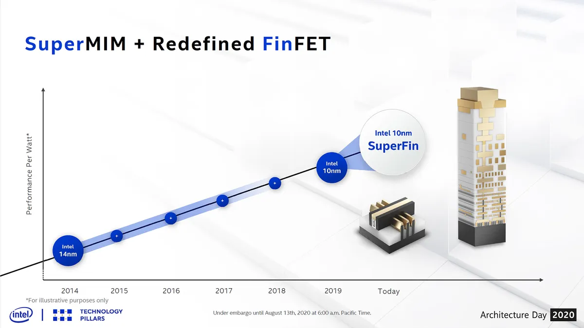
Intel says the new 10nm SuperFin technology provides the largest intra-node performance improvement in the company's history, giving its forthcoming chips higher frequencies and lower power consumption than the first version of its 10nm node. That's a critical need because the company had originally planned for a rapid transition to its 7nm process, leaving its generally unproductive and troublesome 10nm node in the rearview mirror while reserving the node for only a few products as the company quickly moved forward to what it saw as the better node.
To help blunt the blow of the 7nm delay, Intel announced that it would boost its 10nm production by 20% over its prior projections and said it planned to wring out another "full node" of performance from the troubled node. It also plans to leverage its advanced packaging technology to rapidly integrate chips produced at third-party foundries into its own products. Both of these technologies are going to be incredibly important as Intel strives to remain competitive in the face of ever-growing pressure from all sides in its key money-making segments; the desktop PC and data centers. Both segments are now under attack from a resurgent AMD and the burgeoning ARM ecosystem.
Intel's 10nm SuperFin Technology


Intel's plans to wring out more performance from its 10nm aren't entirely surprising - the company learned the value of inter-node improvements the hard way during its incessant 10nm delays. Through a long string of "+" revisions to its 14nm node, with each step powering performance enhancements throughout the Skylake, Kaby Lake, Coffee Lake and Cooper Lake iterations of Intel's chips. Each intra-node step yielded a 3.8% to 5.9% improvement in transistor performance at iso leakage, which translates to tangible performance benefits that helped Intel remain competitive despite its continuous 10nm delays. In fact, Intel claims that it has extracted nearly enough extra performance from 14nm as it has historically gotten from a move to a new, denser process node.
After four intra-node enhancements, much to the amusement and confusion of industry observers, Intel is now on its 14nm++++ node. Intel obviously didn't plan for this many iterations of the node when it first slapped the "+" branding on its first 14nm enhancement, and the scheme has become more than unwieldy. In fact, due to rampant confusion about the naming scheme, including among Intel's own teams, the company will now assign a new unique name to each process node.
"10nm SuperFin" marks the first outing for its new terminology, but Intel says the node is the equivalent of a 10nm+ revision. Intel says that the name "SuperFin" comes from a combination of SuperMIM, one of the key ingredients to the design that we'll cover below, and FinFET, which is Intel's term for its first 3D transistor design that debuted three generations ago and carries on to today.
Intel's inaugural 10nm node encountered plenty of problems, necessitating a lengthy redesign process to fix several not-yet-explained issues. Intel tells us that its currently-shipping version of 10nm still uses Cobalt, Contact Over Active Gate (COAG), and Self-Aligned Quad Patterning (SAQP). This trio of new technologies enabled a 2.7X density improvement over 14nm, but have been rumored to be the source of Intel's delays.


Intel's 10nm SuperFin builds on those technologies with several steps forward of its own. Intel improved the gate pitch to enable higher drive current for some high-speed functions, and enhanced epitaxial growth on the source and drain elements helps lower resistance and improve strain. That helps more current flow through the channel, allowing charge carriers to move more quickly.
The 10nm SuperFin transistors have a new thin barrier that reduces interconnect resistance by 30%, which improves interconnect performance - a critical factor as interconnects continue to shrink and become one of the largest barriers to chip scaling. Intel claims the SuperMIM (Metal-Insulator-Metal) capacitor brings a 5X improvement in MIM capacitance compared to the "industry standard" devices that have the same footprint. This helps combat Vdroop, which helps ensure longer sustained frequency potential. Intel says it used new Hi-K materials stacked in a repeating superlattice structure, and also added two high-performance layers to the top of the stack. The changes don't impact density, but have a big impact on performance.


The 10nm SuperFin transistors offer higher clock speeds at any given voltage, and can operate at a lower voltage at any given frequency. The transistors also have a greater dynamic range from the Vmin to Vmax (minimum/maximum voltage), and Vmax extends further than found with the original 10nm transistors. By tuning the architecture to exploit the full dynamic range of the transistors, Intel claims Tiger Lake offers both higher maximum frequencies in thermally-unconstrained use and is faster and more efficient in TDP-limited environments. Intel says the culmination of the tuning imparts a greater-than-generational performance improvement from the marginally IPC-optimized Willow Cove core over the Sunny Cove cores present in Ice Lake.
Intel says the net effect is the same amount of performance uplift that the company would normally expect from a whole series of intra-node "+" revisions, but with just one iteration. Intel claims these transistors mark the largest single intra-node improvement in the company's history.

Intel famously encountered issues with its original 10nm node that necessitated a redesign, so speculation will run rampant that many of the new features are merely borne of the need to fully correct the issues that hindered first-gen 10nm's performance and profitability.
Regardless, Intel claims to have gained a step-function improvement in the 10nm process node, and the improvements have caught the attention of the company's data center architects. Koduri said that the company is working on a new tentatively-named "Enhanced SuperFin" process, optimized specifically for the data center, that will bring about further performance and interconnect improvements. The latter is an important consideration for data center chips that rely on the utmost bandwidth between compute-heavy cores and heavily-utilized I/O interfaces.
Intel says this process tech will debut with the company's Rambo Cache in its Xe Ponte Vecchio cards and its Sapphire Rapids data center chips.
Decoupling Architecture from Process Nodes
Intel's struggles with its 10nm node led the company to rethink its approach to chip design completely. In the past, Intel's design methodology was focused on single-die monolithic designs with architectures tightly coupled and tuned to each specific process node. Unfortunately, this left the chipmaker exposed to the fallout of any delays in its race to smaller, denser nodes.
Intel is frank that the deep bonds between architectures, IP, and specific process nodes cost it the ability to bring new architectures, like Sunny Cove, to market within a reasonable time frame. Intel also lost the ability to introduce critically important new features in a timely fashion, like PCIe Gen 4, creating deficiencies in its product stack. The lack of flexibility also delayed the rapid development of newer types of products, like its Xe Graphics. The tight coupling between architecture and process nodes also made it nearly impossible to port those designs over to older process nodes, or to shift its designs to nodes from other foundries.
Intel's initial set of contingency plans marked a transformational change to the company's design methodologies. First, Intel committed itself to decoupling its architectures from the process, thus making its architectures portable between nodes. This new approach allows the chipmaker to use newer architectures on older nodes, thus speeding deployment in the face of unanticipated delays. It also allows Intel to select the best node for the intended purpose, be it either an internally-developed node, or a node from an external vendor.
These changes do result in sacrificing some level of deep architectural tuning for each process node, which in turn results in less performance-enhancing customizations. However, the net effect is a faster, more flexible design process that allows the company to sidestep challenges with its process tech.
Intel Advanced Packaging


Intel's advanced packaging technologies will allow it to mix and match IP and process nodes from other vendors into the same heterogeneous packages, yielding time to market advantages. This also reduces the company's investment in certain areas, like external I/O and memory devices, where other vendors have better solutions. The ultimate goal is to blend these different technologies into one package with interconnect performance and bandwidth that either matches or exceeds the performance of a monolithic die.
The idea behind mixing and matching components isn't new to Intel, though: The company began work on its EMIB (Embedded Multi-Die Interconnect Bridge) nearly 20 years ago. This technique uses small silicon bridges embedded into a substrate (deep dive here) to boost performance and reduce cost. After patenting the tech in 2008, Intel moved on to its first high-volume product with Kaby Lake-G. This SoC paired a GPU block Intel purchased from AMD with an HBM stack from another external vendor, proving that Intel could deploy EMIB in tandem with external chiplets in high-volume manufacturing. Intel followed that rollout with its Stratix 10 and Agilex FPGAs, the latter of which can use chiplets from three different foundries, on six different process nodes, in one heterogeneous package.


The standardized AIB (Advanced Interface Bus) interface is the key that unlocks that level of cooperation and integration between so many disparate partners. Intel has worked to further this once-proprietary standard by contributing it to the open-source CHIPS alliance without requiring royalties or licensing, thus allowing other companies to develop chiplets that are compatible with both Intel and others' chiplets.
Intel says the initiative has paid off, with 10 AIB-based tiles from multiple companies are either in production or in the power-up stages of development. The chipmaker also says that 10 more tiles, including from start-ups and universities, are under development. These tiles include such functions as high-speed transceivers, data converters, silicon photonics, and machine learning accelerators. Intel's FPGA's already use chiplets heavily, as they often serve as Intel's lead vehicle for advanced packaging tech. In fact, Intel's next-gen FPGAs will be the first large devices to use Foveros 3D packaging (details are slim).
Intel says that AIB 2.0 will arrive in early 2021 and that it has already open-sourced an AIB generator that uses industry-standard PDKs, thus enabling the rapid generation of custom IP blocks.
The key takeaway here is that Intel's efforts in forging an industry-standard chiplet interface are moving along well, with AIB 2.0 offering three times the bandwidth, much lower bump densities, higher bandwidth density, lower voltage, and more energy efficiency - all in a standard that is backward compatible with AIB 1.0.


Intel also has its 3D Foveros technology, which allows logic-on-logic die stacking, and its Co-EMIB interconnect that is a combination of EMIB and Foveros that allows for connecting multiple 3D-stacked die packages. ODI and MDIO packaging also weigh in, all of which you can read about here.
Even with all of these various technologies, Intel revealed one final new addition at its Architecture Day: Hybrid Bonding. This technique allows for die-on-wafer hybrid bonding as an alternative to traditional thermo-compression bonding. This new technique features aggressive bump pitches (which increases interconnect density), simpler interconnect circuitry, and lower capacitance and power consumption - all with higher bandwidth. Intel says it has already taped out a stacked SRAM chip with Hybrid Bonding, so we expect to learn more about this technology soon.

As with all semiconductor technologies, the path to interconnect scaling comes through smaller feature sizes, like improved bump pitch and density, which also helps to reduce power consumption. Intel's final packaging technology roadmap lists aggressive future targets for EMIB and Foveros and also teases the Hybrid Bonding specs compared to the other interconnects.
Intel says Hybrid Bonding will scale to a sub-10 micron bump pitch with a bump density of 10,000 mm^2, which is far more impressive than the targets for the existing interconnects. The tech also aims to conduct data transfers at an almost unimaginably-low power consumption of 0.05 pJ/bit, signaling that Intel has ambitious targets for the future of its interconnect technologies.
While Intel is busy developing its newer forms of interconnects, its EMIB technology and the AIB interface has now become proven and mature in the market. We expect Intel will look to leverage this packaging tech, perhaps in tandem with Foveros, as it begins integrating more chiplets into its own designs. Those chiplets could even include Intel's own architectures etched on someone else's process node as it looks to create stopgap products as recovers from its delayed 7nm node.
