Intel Video Shows How It Makes a 10nm Processor
From sand to shipping silicon...finally

Intel has released two videos about its chip design and manufacturing process that give us a rare glimpse into not only the company's production process, but also into its problematic 10nm process.
Intel's woes with the 10nm process are well-documented. The company has suffered almost incalculable damage to its long-term roadmaps due to the delay of mass production of its newest node, and even recently cited that it didn't expect to reach parity with its competitors (most likely in reference to third-party foundry TSMC) until it releases its 7nm process at the end of 2021.
The world of processor design is fraught with technical challenges, and long design cycles are problematic: It can take up to four years from the design stage to final production. As an engineer once quipped, designing a chip is like playing Russian roulette and waiting four years to see if you've blown your brains out. But that didn't stop Intel from plowing forward with audacious goals for its 10nm process. Intel bet big when it began the 10nm design, eschewing the standard doubled gen-on-gen density by aiming for a 2.7X density increase. The company later cited that goal as a key reason it struggled with 10nm, largely because the density goals required several new technologies that contributed to the delays. We can see a few of those potential missteps in the video below.
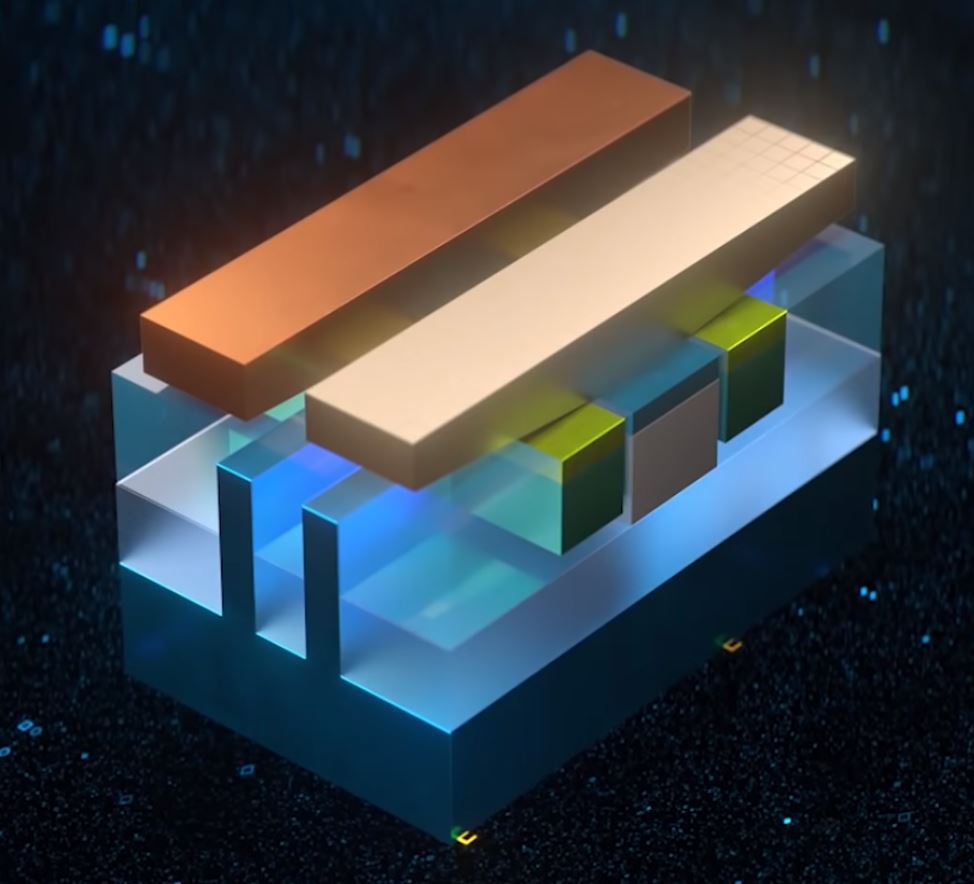
The video covers the manufacturing process "from sand to silicon," and while all of it is worth a watch, the deep dive into Intel's transistor tech begins at roughly 1:50 into the video. Here the company details its FinFET transistor technology and outlines the stunning number of steps required to build up a single transistor (more than a 1000). However, these photolithography, etch, deposition, and other steps are applied to an entire wafer that has multiple die that each wield billions of transistors.
Intel details its contact over active gate (COAG) technology at 3:10 in the video. This tech builds the contact portion of the transistor over the gate instead of extending it from the end of the transistor as Intel has done in the past. That reduces the overall area consumed by the transistors, thereby improving density (more details here at WikiChip). Intel is rumored to have altered, or perhaps even removed (which is unlikely), its COAG feature from its newer iterations of the 10nm process. This part of the design is key, as it helps dictate the performance of transistors that switch on and off at a rate exceeding five billion cycles a second with the 14nm process, but those speeds fall considerably with the 10nm process.
The video also gives us a glimpse of the dizzyingly-complex web of interconnects present on the chip. These tiny wires connect the amazingly-small transistors together, facilitating communication, and are stacked in a complex 3D cluster. However, these small wires can be mere atoms thick, which can lead to failure-inducing electromigration. Smaller transistors require thinner wires, but that also leads to increased resistance that requires more current to drive a signal, which complicates matters. To tackle that challenge, Intel switched from copper wiring to cobalt. Intel used this material to create thinner wires (even though it has higher resistivity) because it doesn't require as much insulation material wrapped around each wire, but the company only uses it at the lowest levels of the 3D web of interconnects. However, the switch to cobalt is yet another challenge that is rumored to be at the root of Intel's troubles.
Intel has divulged that it significantly overhauled the 10nm process to address unspecified issues, but we'll likely never know the full extent of those changes. At the end of the day, however, economical production is the true measure of success, and that is often measured by the yield rate (ie, how many functional chips are harvested per wafer). Intel has struggled in this area, and even by its own projections won't reach parity on process nodes until 2021. In the meantime, the company is looking to its new technologies that aren't entirely contingent upon process leadership, like EMIB and Foveros, and it plans to adopt new chiplet-based architectures. We also expect Intel will continue to work on making its architectures portable across nodes to blunt the blow from potential future missteps.
Get Tom's Hardware's best news and in-depth reviews, straight to your inbox.
But Intel's primary challenger, AMD, is also focused on next-gen packaging and fabrics to extend its own chiplet-based architecture, so competition will be brisk. Meanwhile, multiple ARM-based server chips now benefit from TSMC's node, which threatens further margin erosion and makes Intel's ability to adhere to an H2 2020 schedule for its Ice Lake chips imperative.
The world of processor design is a minefield of technical challenges, but the intricacies of a chip are truly a modern marvel. We'd love to see more detailed videos of the inner workings of other modern process nodes, in particular the 7nm node from TSMC.
While we wait, Intel also posted another chip manufacturing video that's decidedly more basic and obviously geared for mainstream audiences. Check it out below.

Paul Alcorn is the Editor-in-Chief for Tom's Hardware US. He also writes news and reviews on CPUs, storage, and enterprise hardware.
