Intel Unveils Sunny Cove, Gen11 Graphics, Xe Discrete GPU, 3D Stacking
3D Chip Stacking With Foveros
Foveros (Greek for "awesome") is a new 3D packaging technology that Intel plans to use to build new processors stacked atop one another. The concept behind 3D chip stacking is a well-traveled topic that has been under development for decades, but the industry hasn't been able to circumvent the power and thermal challenges, not to mention poor yields, well enough to bring the technology to high-volume manufacturing.

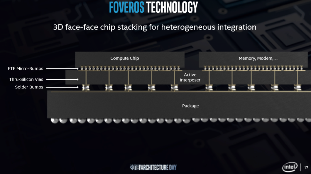
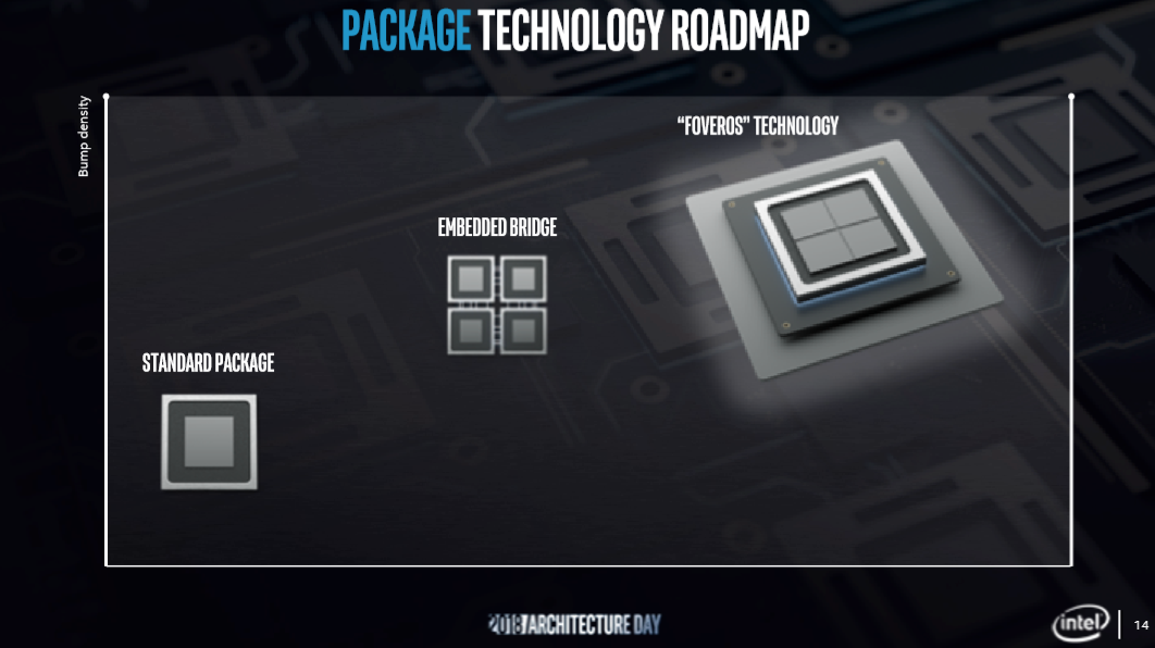

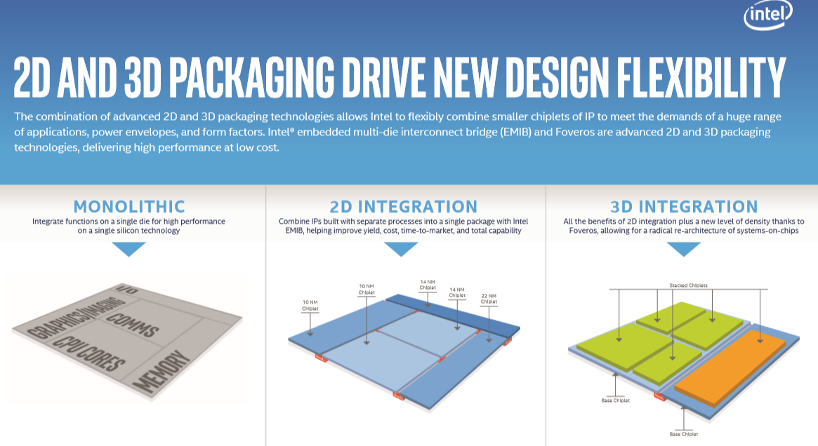


Intel says it built Foveros upon the lessons it learned with its innovative EMIB (Embedded Multi-Die Interconnect Bridge) technology, which is a complicated name for a technique that provides high-speed communication between several chips. That technique allowed the company to connect multiple dies together with a high-speed pathway that provides nearly the same performance as a single large processor. Now Intel has expanded on the concept to allow for stacking die atop each other, thus improving density.
The key idea behind chip stacking is to mix and match different types of dies, such as CPUs, GPUs, and AI processors, to build custom SOCs (System-On-Chip). It also allows Intel to combine several different components with different processes onto the same package. That lets the company use larger nodes for the harder-to-shrink or purpose-built components. That's a key advantage as shrinking chips becomes more difficult.
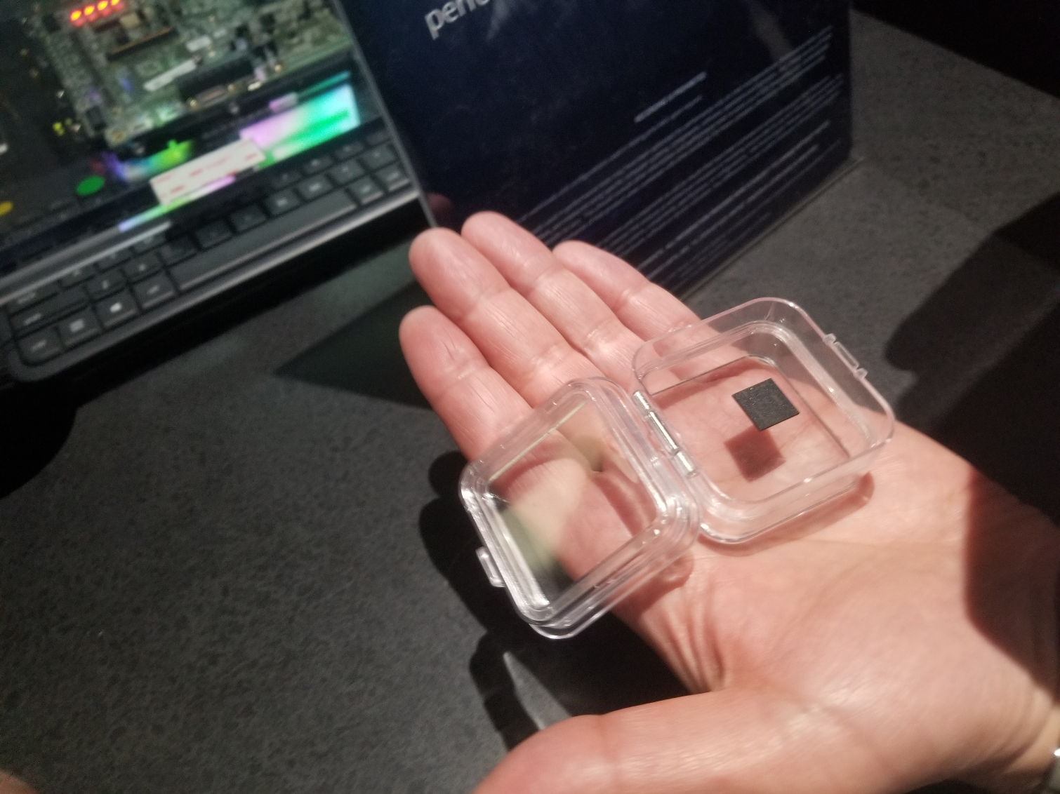

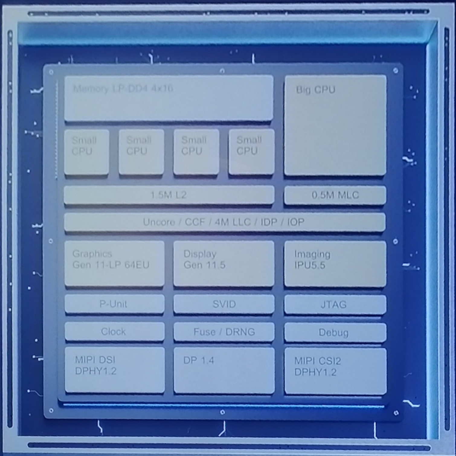
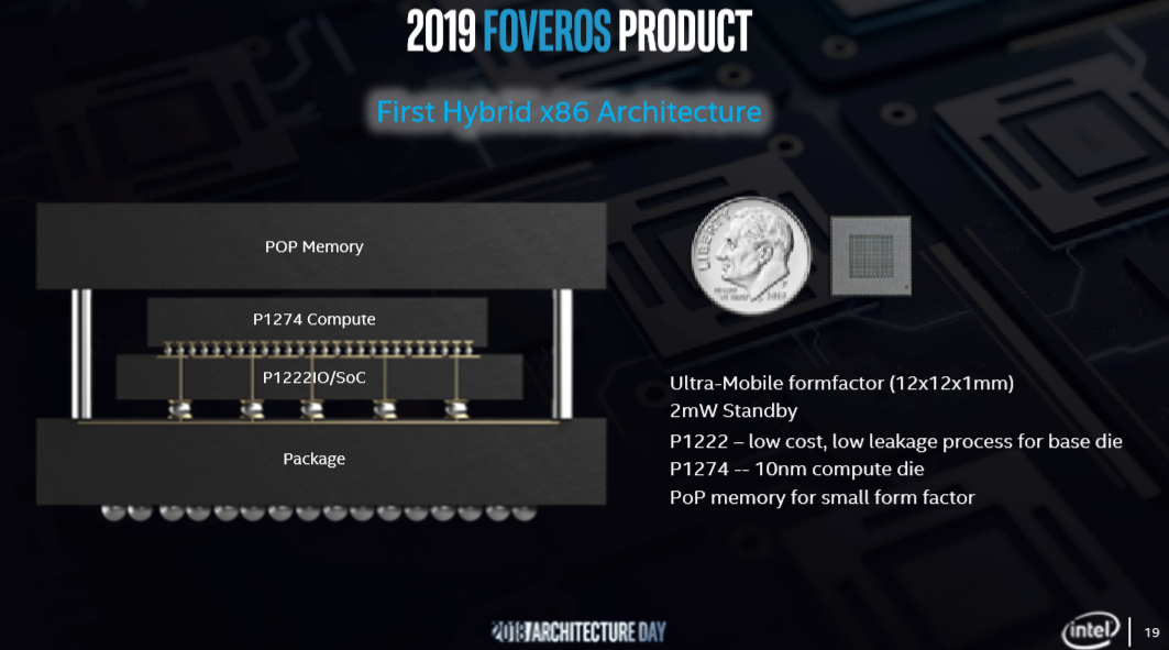
Intel had a fully functioning Foveros chip on display at the event, that it built for an unnamed customer. The package consists of a 10nm CPU and an I/O chip. The two chips mate with TSVs (Through Silicon Via) that connect the die through vertical electrical connections in the center of the die. The channels then mate with microbumps on an underlying package. Intel also added a memory chip to the top of the stack using conventional a PoP (Package on Package) implementation. The company envisions even more complex implementations in the future that include radios, sensors, photonics, and memory chiplets.
The current design consists of two dies. The lower die houses all of the typical southbridge features, like I/O connections, and is fabbed on the 22FFL process. The upper die is a 10nm CPU that features one large compute core and four smaller 'efficiency' cores, similar to an ARM big.LITTLE processor. Intel calls this a "hybrid x86 architecture," and it could denote a fundamental shift in the company's strategy. The company later confirmed that it is working on building a new line of products based on the new hybrid x86 architecture, which could be the company's response to the Qualcomm Snapdragon processors that power Always Connected laptops. Intel representatives did confirm the first product draws less than 7 watts (2mW standby) and is destined for fanless devices but wouldn't elaborate further.
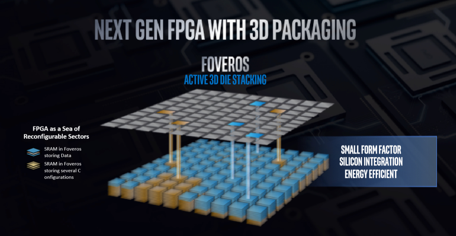
The package measures 12x12x1mm, but Intel isn't disclosing the measurements of the dies. Stacking small dies should be relatively simple compared to stacking larger dies, but Intel seems confident in its ability to bring the technology to larger processors. Ravishankar Kuppuswamy, Vice President & General Manager of Intel's Programmable Solutions Group, announced that the company is already developing a new FPGA using the Foveros technology. Kuppuswamy claims Foveros technology will enable up to two orders of magnitude performance improvement over the Falcon Mesa FPGAs.
Get Tom's Hardware's best news and in-depth reviews, straight to your inbox.
Current page: 3D Chip Stacking With Foveros
Prev Page Intel Architecture Day Next Page Intel Xe Discrete Graphics and Gen11 Graphics
Paul Alcorn is the Editor-in-Chief for Tom's Hardware US. He also writes news and reviews on CPUs, storage, and enterprise hardware.
