Intel Foundry Roadmap Update - New 18A-PT variant that enables 3D die stacking, 14A process node enablement
Smaller, faster, better.
Intel's new CEO Lip Bu-Tan took to the stage at the company's Intel Foundry Direct 2025 event here in San Jose, California, to outline the company's progress on its foundry initiative. Tan announced that the company is now engaging lead customers for its upcoming 14A process node (1.4nm equivalent), the follow-on generation of its 18A process node. Intel already has several customers with plans to tape out 14A test chips, which now come with an enhanced version of the company's backside power delivery technology dubbed PowerDirect. Tan also revealed that the company's crucial 18A node is now in risk production with volume manufacturing on schedule for later this year.
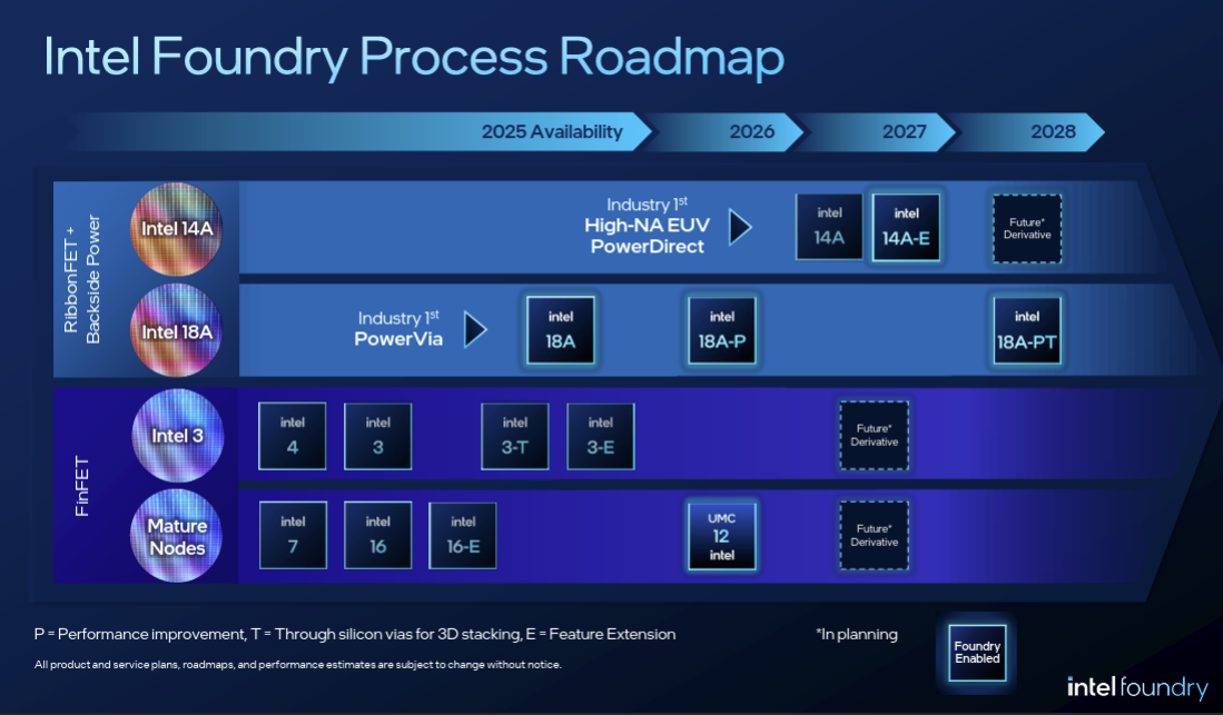
Intel also revealed that its new 18A-P extension, a high-performance variant of the 18A node, is now running through the fab with early wafers. Additionally, the company is developing a new 18A-PT variant that supports Foveros Direct 3D with hybrid bonding interconnects, enabling the company to stack dies vertically on top of its most advanced leading-edge node.
The Foveros Direct 3D technology is a key development because it provides a capability that rival TSMC already uses in production, most famously in AMD's 3D V-Cache products. In fact, Intel's implementation matches TSMC's offering in critical interconnect density measurements.
Article continues belowOn the mature-node side of the operation, Intel Foundry has its first production 16nm tapeout in the fab now, and the company is also now engaging customers for the 12nm node it is developing in partnership with UMC.
Perhaps the most important developments at the show revolve around Intel's continued expansion with EDA and intellectual property (IP) partners that provide the critical tools and IP blocks that enable its customers to develop new designs with industry-standard design flows and tools. The company has also expanded its Intel Foundry Accelerator Alliance program to include the Chiplet Alliance and Value Chain Alliance programs.
Intel Foundry's progress comes during turbulent times in the semiconductor industry as geopolitical divisions threaten to fracture the global chip supply chain. Intel is currently the only US-based domestic supplier of leading-edge process node technology and advanced packaging capacity, a key advantage as tensions between China and TSMC continue to escalate. Despite TSMC's expansion of production in the US, a recent law passed by Taiwan now prevents the company from producing its most cutting-edge tech in the United States, leaving Intel as the only domestic foundry with both leading-edge chip production and R&D.
Naga Chandrasekaran, the Chief Technology and Operations Officer of Intel Foundry, and Kevin O’Buckley, the General Manager of Foundry Services, are also slated to deliver keynotes during the event, providing more details about the technology and roadmaps. We will update this article with additional information as it becomes available, but we have plenty to share to get started. Let's take a closer look at Intel's progress.
Get Tom's Hardware's best news and in-depth reviews, straight to your inbox.
Intel 14A Process Node
Intel 14A Process Node
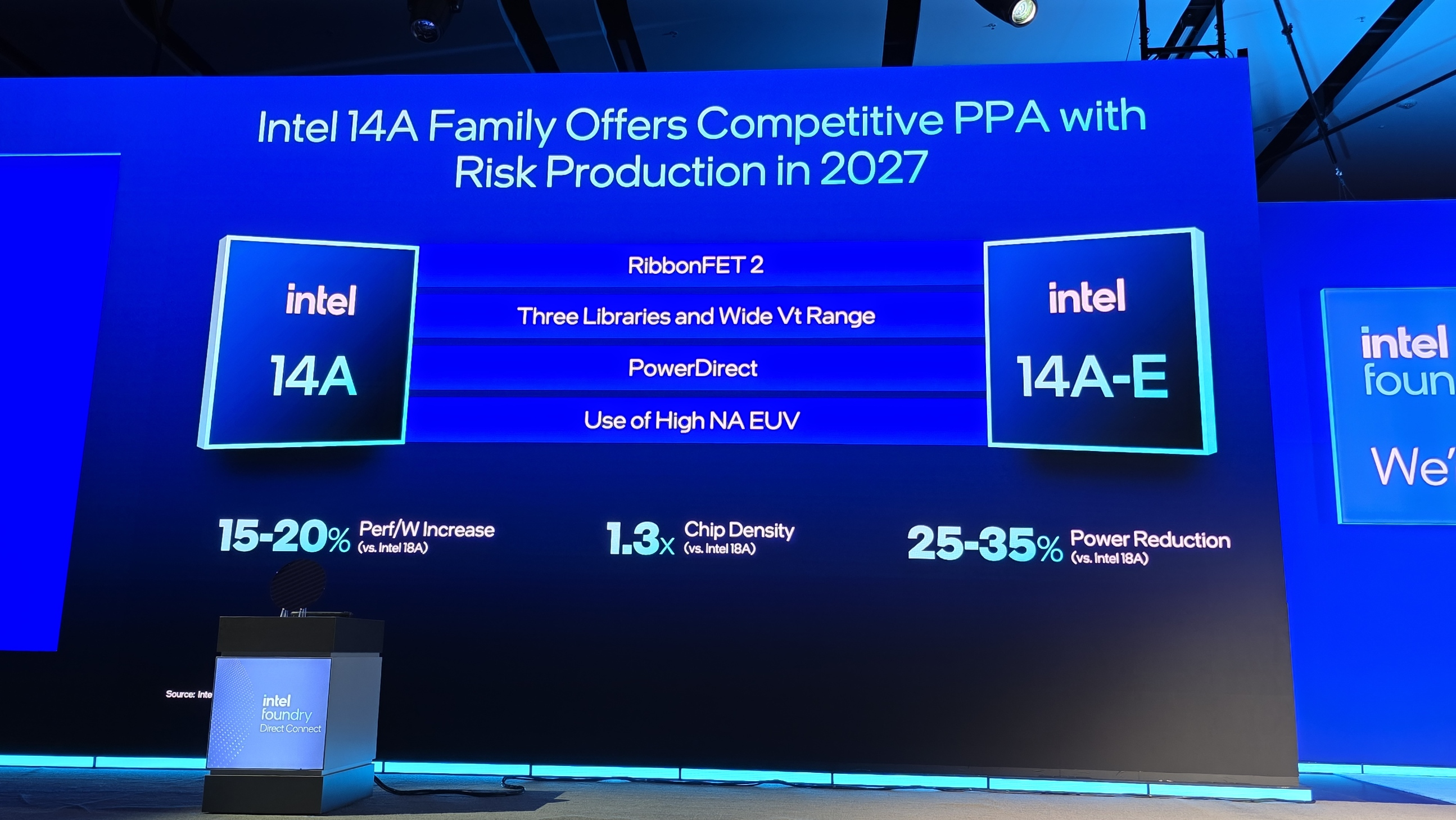
Intel's 14A, the next generation after 18A, is already in the works and scheduled for risk production in 2027. If all goes to plan, 14A will be the industry's first node to employ High-NA EUV lithography. TSMC's competing A14 (1.4nm-class) node is expected to arrive in 2028, but the Taiwanese company will not utilize High-NA for production.
Intel has already shared early versions of the Process Design Kit (PDK), a set of data, documentation, and design rules that enables the design and validation of a processor design, with its lead 14A customers. Intel states that multiple customers have already indicated their intention to build chips using the 14A process node.
Intel's 14A will have a second-generation version of its PowerVia backside power delivery technology. The new PowerDirect implementation is a more advanced and complex scheme that delivers power directly to each transistor's source and drain through specialized contacts, which minimizes resistance and maximizes power efficiency. This is a more direct and efficient connection than Intel's current PowerVia scheme, which connects to the contact level of the transistors with Nano TSVs.
TSMC's N2 node does not include backside power delivery; however, with A16, the company will employ a direct-contact backside power delivery network, dubbed Super Power Rail (SPR). A16 is essentially a derivative of the N2P node with SPR. The A16 node is expected to enter production in late 2026. TSMC's A14 will not leverage a backside power design methodology.
Intel's 18A-PT process node enables die stacking
Intel's 18A-PT process node enables die stacking
Intel's 18A node is the mainstream variant, but the company also has several 'line extensions' of the node, designated by different suffixes. These flavors of the underlying node are tailored for different use cases.
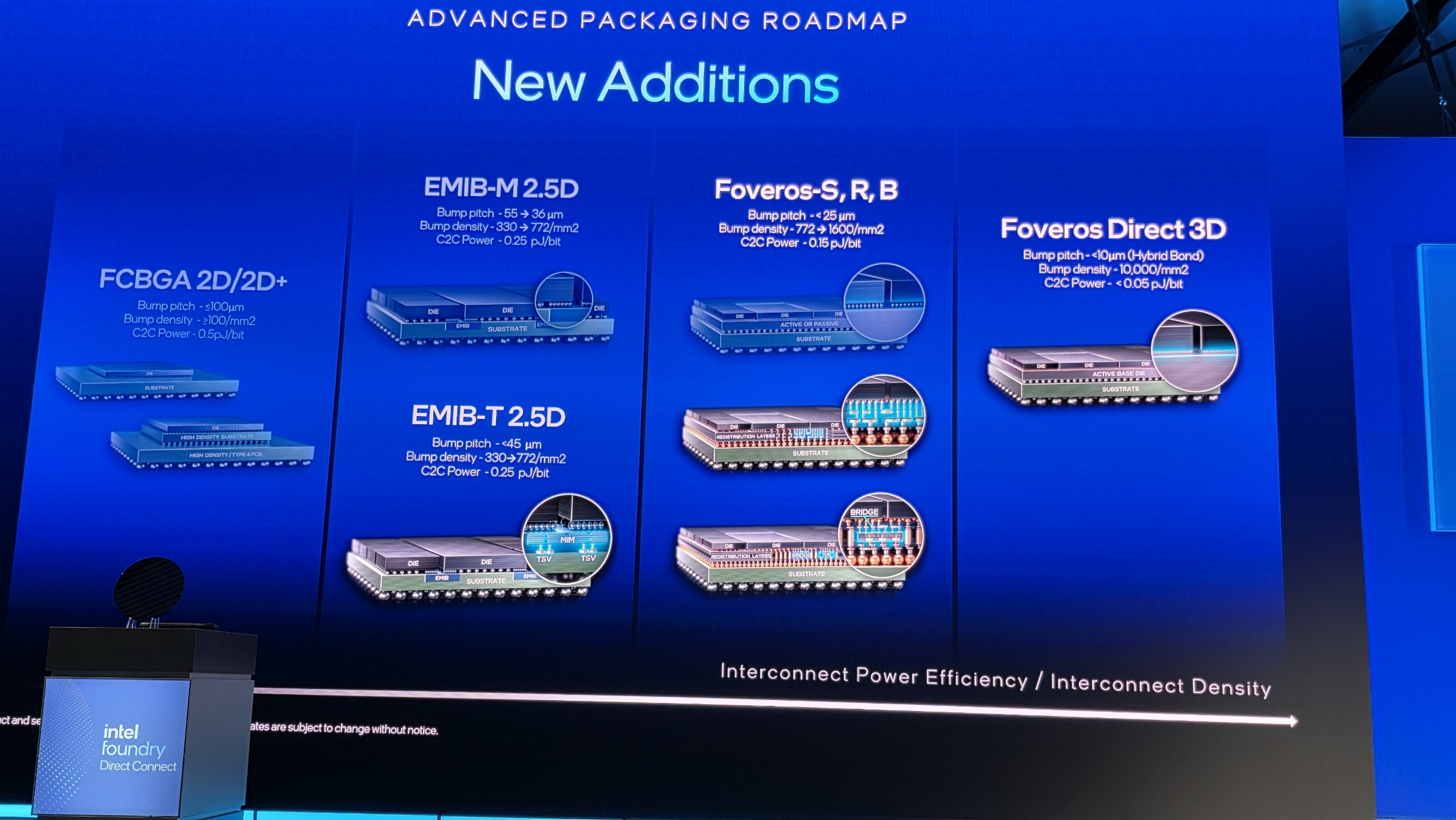
Intel has a new 18A variant up its sleeve; the new 18A-PT node that will provide the same performance and efficiency benefits as the performance-oriented 18A-P, but adds in Foveros Direct 3D hybrid bonding. This bump-less copper-to-copper bonding technique (meaning it doesn't use microbumps or solder to connect the two dies) fuses chips together with through-silicon vias (TSVs). Intel's implementation will employ a pitch of less than 5 microns, a distinct improvement over its initial goal of a 10um pitch by 2023, to fuse chiplets on top of the 18A-PT die. The pitch is a measurement of the center-to-center spacing between the interconnects, and lower values indicate higher density, which is better.
Notably, AMD uses TSMC's SoIC-X technology, a similar hybrid bonding approach, to fuse an L3 chiplet atop its X3D processors with a 9 micron bump pitch. TSMC's SOIC-X tech currently ranges from 4.5 to 9 microns, but the company has a 3-micron pitch offering on the roadmap for 2027. If productized effectively and on schedule, Intel's Foveros Direct 3D will dramatically improve its positioning against TSMC's packaging technology.
Intel's Clearwater Forest will be its first to use Foveros Direct 3D packaging, but the company hasn't disclosed the pitch for that specific product yet. Notably, TSVs are typically only included in the base die, and Clearwater Forest uses Intel 3-T for the base die with the Intel 18A compute dies stacked on top. Enabling TSVs for 18A will thus allow it to also have dies stacked atop, and SRAM cache is a logical use case.
Intel 18A process node updates
Intel 18A process node updates
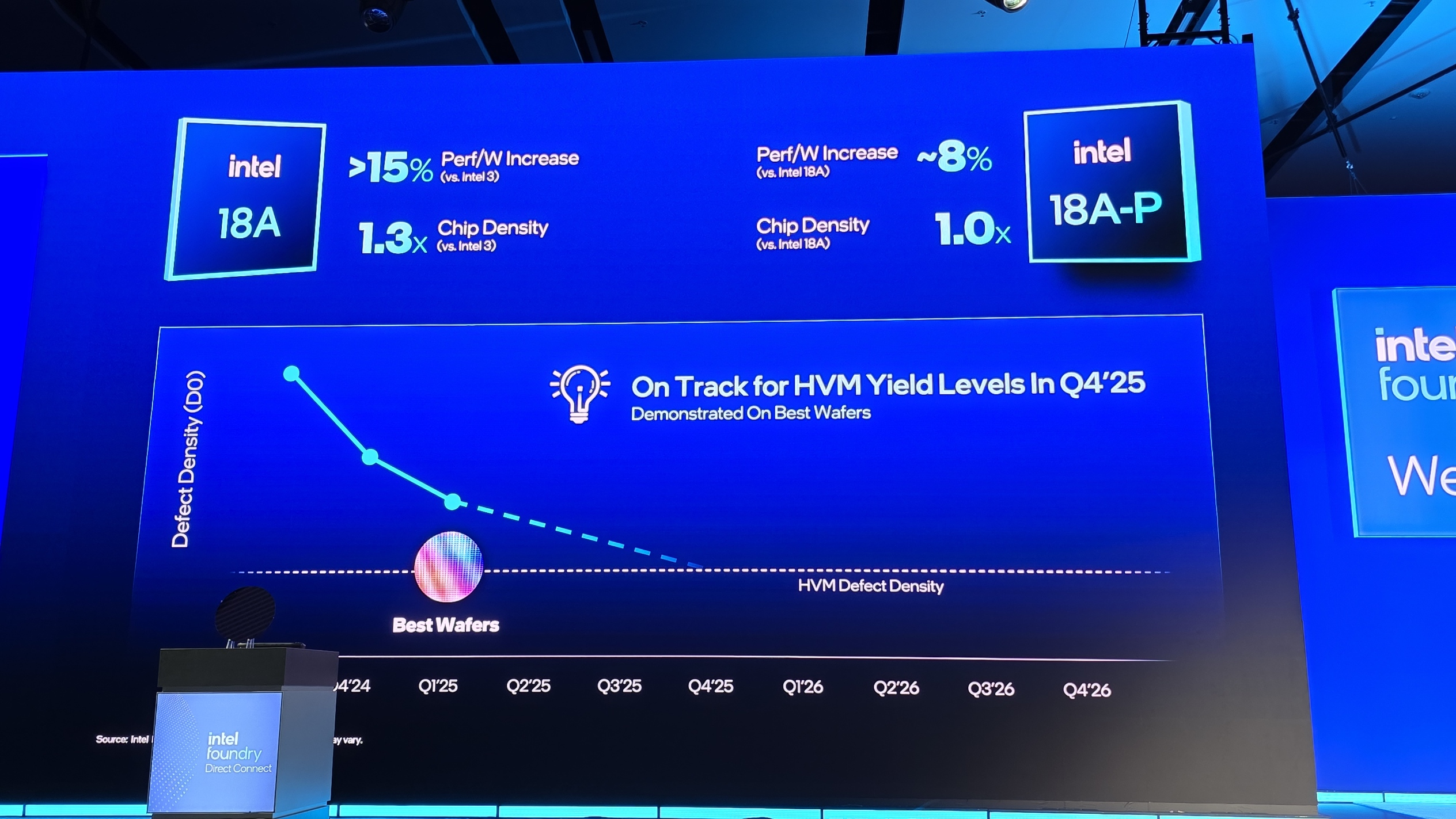
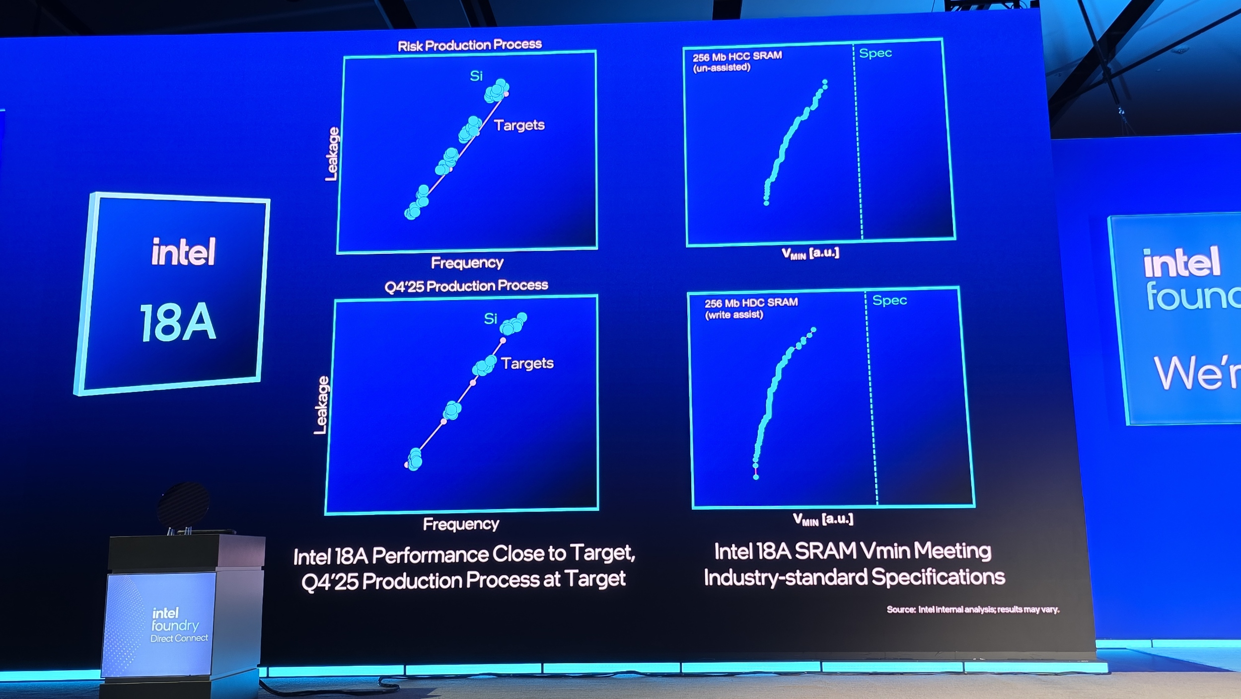
As we reported last month, Intel's 18A (1.8 nm-equivalent) process node has entered risk production, marking the commencement of the first low-volume production runs of the node, with High Volume Manufacturing (HVM) scheduled for the end of the year. Intel did not specify which processors had begun production, but the timing generally aligns with expectations for its Panther Lake processors, which are expected to arrive at the end of the year. Intel's first 18A production will come from its Oregon fabs, but the company has already 'run the [18A] lot' through its Arizona fab, indicating it will soon begin production there as well.
The 18A node is the first in the industry to be productized with both a PowerVia backside power delivery network (BSPDN) and RibbonFET gate-all-around (GAA) transistors. PowerVia provides optimized power routing on the back of the chip to improve performance and transistor density. RibbonFET also offers better transistor density, along with faster transistor switching, in a smaller area through the use of four vertical nanosheets surrounded entirely by the gate.
The 18A node enters HVM in roughly the same timeframe as TSMC's competing 2nm N2 node. However, TSMC's N2 node does not come with a backside power delivery network, but it does have GAA technology with three vertical nanosheets. There have been some basic comparisons between the process nodes made based on presentations at a recent industry event. The general takeaway is that Intel's node is faster and lower-power than TSMC's, though TSMC retains the edge in density (and presumably cost). However, these distinctions could vary depending on the specific implementation in different chip designs.
Intel divulged today that it has wafers of its high-performance 18A-P node in the fab. This 18A variant features an optimized power and frequency curve, providing an 8% improvement in performance per watt. This can be leveraged as either higher clock speeds or lower power consumption at the same performance, depending upon chip-specific tuning.
The 18A-P node is design rule-compatible with the 18A node, easing the design process for customers. Intel is already collaborating with Electronic Design Automation (EDA) software vendors to enable broad support for industry-standard design tools, and it is also working with Intellectual Property (IP) designers to provide the necessary IP blocks, thereby simplifying implementation.
Mature Nodes: 16nm and 12nm continue advancing
Mature Nodes: 16nm and 12nm continue advancing
Intel Foundry not only addresses the leading edge of technology, but it is also working on several mature nodes. Intel's 16nm node, which is essentially a version of its 22FFL node that leverages industry standard design tools and PDKs, has a tapeout in the fab now.
Intel is also continuing its work with partner UMC to develop a 12nm node that will be produced in three of Intel's Arizona fabs beginning in 2027. In fact, Intel is currently engaging lead customer for this node. 12nm will be used primarily for mobile communication infrastructure and networking applications.
Takeaways, for now
Takeaways, for now
Intel canceled high volume manufacturing of the 20A node as a cost-cutting measure, but the company is now on the cusp of of production with with its18A node, marking a critical milestone as it looks to regain the manufacturing lead over TSMC. The addition of new line extensions, with the die-stacking-capable 18A-PT being a particularly strong advance, will help the company to further broaden its appeal to potential foundry customers.
The development of the company's 14A node is also well underway, signifying that the company is on track to providing a steady cadence of new nodes and features to the roadmap. We haven't yet heard any new details about Intel's plans for its 10A (1nm-class) process node yet, which is expected to begin development in 2027. Intel's press release also doesn't mention any new progress on its Intel 3 node, but we expect more details to emerge throughout the day.
Intel's event is focused heavily on displaying its broad portfolio of EDA, IP, and services driven by an ecosystem of indsutry stalwarts, like Synopsys and Cadence. The new Intel Foundry Chiplet Alliance is also an important development that will enable customers to mix-and-match chiplets into their design based upon interoperable and validated designs.
Intel's advanced packaging services are also of particular importance as they provide the fastest on-ramp to meaningful revenue generation. Intel did mention that it will make its 3D stacking Foveros implementation available to foundry customers, and noted a new partnership with Amkor. However, details are slight for now. We'll update this article as more information becomes available.

Paul Alcorn is the Editor-in-Chief for Tom's Hardware US. He also writes news and reviews on CPUs, storage, and enterprise hardware.
-
Heiro78 I don't get the naming scheme. I woulda thought the lower the number the better/ smaller architectureReply -
EzzyB I keep hearing that 18A is "faster, but less dense." I know the site is almost exclusively interested in whatever is faster! 😁 What is the use case for something that's maybe not quite as fast, but more dense. Just size of the chip? More space for more things on the chip? Maybe cheaper to make?Reply -
EzzyB Reply
Oh that one is easy. Let the old timer tell you! 😜Heiro78 said:I don't get the naming scheme. I woulda thought the lower the number the better/ smaller architecture
In the old days "NM" was the measure, in nanometers, of the separation of different components, mainly transistors on a chip. I say the old days because "NM" ceased to have any real meaning around the turn of the century (300 NM nodes.) So that is the standard that was set, and then broken long ago.
Notice in the article Tom's says something like "2nm equivalent." That's because 1.8A of 2.0 or whatever aren't really accurate anymore. It's marketing.
A half decade ago or so there was a big hullabaloo about how TMCS had advanced to "7nm", but Intel was stuck on "10 NM". But, if you looked at the chips, while not exactly the same, they were, in fact quite comparable.
So, in the beginning the naming scheme was about the size of features on the chips. The smaller the size the more features you could put on the chip. But, as I said. It's really misleading now. I think we're actually somewhere around 17-20 actual nanometers still even though the branding has gotten away from all companies involved. -
DS426 Reply
Yes, probably more focus on chip features and definitely size of the chip where taking up space on advanced node wafers is getting more and more expensive. This would mean that performance optimization would literally come at the trade-off of higher cost.EzzyB said:I keep hearing that 18A is "faster, but less dense." I know the site is almost exclusively interested in whatever is faster! 😁 What is the use case for something that's maybe not quite as fast, but more dense. Just size of the chip? More space for more things on the chip? Maybe cheaper to make? -
User of Computers Didn't seem to affect the stock price much lol. Guess investors don't really care about the progress?Reply -
Pierce2623 Reply
GPUs would be better on “denser but not quite as fast”.EzzyB said:I keep hearing that 18A is "faster, but less dense." I know the site is almost exclusively interested in whatever is faster! 😁 What is the use case for something that's maybe not quite as fast, but more dense. Just size of the chip? More space for more things on the chip? Maybe cheaper to make? -
-Fran- Hm... Does the market and investors even believe this?Reply
I'm not asking that in a sarcastic or mean way. I honestly don't know (or think) if people believe Intel can pull this aggresive roadmap, because it is rather aggressive.
Regards. -
TerryLaze Reply
What do you think is aggressive about it?!-Fran- said:Hm... Does the market and investors even believe this?
I'm not asking that in a sarcastic or mean way. I honestly don't know (or think) if people believe Intel can pull this aggresive roadmap, because it is rather aggressive.
Regards.
New node two years after the previous one, that's pretty normal. -
jkflipflop98 Reply
I've learned a long time ago that investors and analysts are pretty much idiots. They have no idea what's going on. I read "expert analyst" blurbs all the time and they're so far off the target that I can't help but to laugh. And those are the people the investors are listening to. It's literally the blind leading the blind.User of Computers said:Didn't seem to affect the stock price much lol. Guess investors don't really care about the progress? -
jkflipflop98 Reply
For the longest time, the nm metric described the distance from the contact points on the transistor - basically the size you could make the entire transistor. Then at some point in the 2000's it kind of morphed to the smallest structure you could fab. Then it turned into the width of the smallest line you could lithographically imprint. Now it's just lost all meaning whatsoever. Intel was the last holdout that actually measured from contact to contact. We stopped doing that with 7nm and just started going with the flow. If everyone else is going to lie, may as well follow suit.Heiro78 said:I don't get the naming scheme. I woulda thought the lower the number the better/ smaller architecture