
We've already covered the first major announcements from the Intel Foundry Direct Connect event, but it turns out that Intel miscommunicated about a presentation that was thought to be under NDA — now Intel says the presentation is open to be reported to the public, so we have some more news to share: Intel's previously-unannounced Intel 10A (analogous to 1nm) will enter production/development in late 2027, marking the arrival of the company's first 1nm node, and its 14A (1.4nm) node will enter production in 2026. [Edit: to be clear, this means 10A is beginning development, not entering high volume manufacturing, in 2027] The company is also working to create fully autonomous AI-powered fabs in the future.
Intel's Keyvan Esfarjani, the company's EVP and GM and Foundry Manufacturing and Supply, held a very insightful session that covered the company's latest developments and showed how the roadmap unfolds over the coming years.
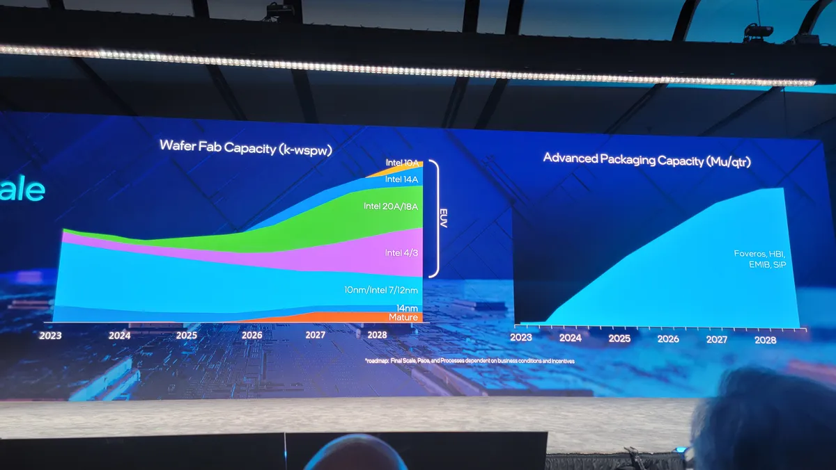

Here, we can see two charts, with the first outlining the company's K-WSPW (thousands of wafer starts per week) capacity for Intel's various process nodes. Notably, capacity typically indicates how many wafers can be started, but not the total output — output varies based on yields. You'll notice there isn't a label for the Y-axis, which would give us a direct read on Intel's production volumes. However, this does give us a solid idea of the proportionality of Intel's planned node production over the next several years.
Intel did not specify the arrival date of its coming 14A node in its previous announcements, but here, the company indicates it will begin production of the Intel 14A node in 2026.
Even more importantly, Intel will begin production/development of its as-yet-unannounced 10A node in late 2027, filling out its roster of nodes produced with EUV technology. Intel's 'A' suffix in its node naming convention represents Angstroms, and 10 Angstroms converts to 1nm, meaning this is the company's first 1nm-class node.
Intel hasn't shared any details about the 10A/1nm node but has told us that it classifies a new node as at least having a double-digit power/performance improvement. Intel CEO Pat Gelsinger has told us the cutoff for a new node is around a 14% to 15% improvement, so we can expect that 10A will have at least that level of improvement over the 14A node. (For example, the difference between Intel 7 and Intel 4 was a 15% improvement.)
Capacity for the Intel 4 and Intel 3 processes doesn't build as quickly as 20A/18A, but that isn't surprising — the majority of the company's wins for its third-party foundry business have been with the 18A node, which Intel says is according to plan. As shown, Intel will also steadily draw down its overall production of its 14nm, 10nm, Intel 7, and 12nm nodes as it transitions to the EUV-enabled nodes.
Notably, Intel's slide has a footnote that says, "*roadmap: Final Scale, Pace and Processes dependent on business conditions and incentives," mirroring the company's ongoing statements that funding from the CHIPS Act will impact its ability to scale production.
Intel's 18A and 20A nodes have been in at least some form of production since 2023, which isn't too surprising — the company won a RAMP-C contract for 18A with the US government back in 2021, and companies like IBM, Microsoft, and Nvidia have been working on generating test chips since (Understandably, Intel will not share details with the public, but it has won a $1 billion award from the US Government for the program).
Additionally, Intel's 20A finds the company integrating two new technologies at once - backside power (PowerVIA) and GAA transistors (RibbonFET). To de-risk the process and avoid stumbles like it saw with 10nm, Intel announced in April of 2022 that it had run a different flavor of 20A through its fabs, an internal test node with only backside power paired with standard FinFETs, to ensure backside power worked separately before being integrated into the final 20A node. As such, we can expect that 20A wafers have been flowing through an Intel fab for quite some time.
As shown on the right, Intel will also aggressively ramp up its advanced packaging production capacity for Foveros, EMIB, SIP (silicon photonics), and HBI (hybrid bond interconnect). Advanced packaging capacity has been a key choke point for the current shortages of AI accelerators. This increased capacity will ensure a steady supply of advanced processors with complex packaging, including HBM.
Intel's ramp of advanced packaging capacity is explosive — the company had very little production capacity for these interconnects in 2023. As an aside, Intel recently wrapped up all of its internal packaging efforts using standard packaging; it is now all-in on advanced packaging and will use OSATs (outsourced assembly and test companies) for standard packaging tasks.
The second slide in the above album visualizes how Intel's move to operating as an external foundry will allow it to increase both the amount of production for each of its nodes and the length of time that each node is in production, thus maximizing profit from its fab and equipment expenditures as it serves its customer orders over longer periods.


Esfarjani also shared details about Intel's globe-spanning operations. In addition to its existing facilities, the company plans to invest $100 billion over the next five years on expansions and new production sites.
The slides above outline the various locations of node production, with 18A occurring in Fab 52 and 62 in Arizona. In contrast, the advanced packaging and 65nm foundry operations for Tower will occur in Fab 9 and 11X in New Mexico. Intel didn't share where it plans to produce its 10A node, and it also has ongoing expansions in Ohio, Israel, Germany, Malaysia, and Poland.
This geographically distributed production capacity, spanning both chipmaking and packaging, allows Intel to have global redundancy in its operations while also offering its foundry customers the option of leveraging a supply chain entirely located in America.


As we illustrated in our coverage of our tour of Intel's Penang, Malaysia facilities, the company leans heavily on automation in its foundries. Intel now plans to use AI in all segments of its production flows, from capacity planning and forecasting to yield improvements and actual floor-level production operations, in a '10X moonshot' effort.
Esfarjani didn't provide a timeline for the company's moonshot effort but said it will impact every aspect of its operations in the future. That includes the introduction of AI "Cobots," which are collaborative robots that can work along with humans, and extensive robotic automation in the manufacturing process.
In the meantime, Intel will continue to aggressively pursue any and all potential customers for its operations. You can read more about those efforts in our interview with Stu Pann, the SVP and GM of Intel Foundry Services, who is tasked with making Intel Foundry the world’s second-largest foundry by 2030.
