Inside Intel's CPU Packaging Factory: From Wafer to Chip
Touring Intel's Malaysian facilities.
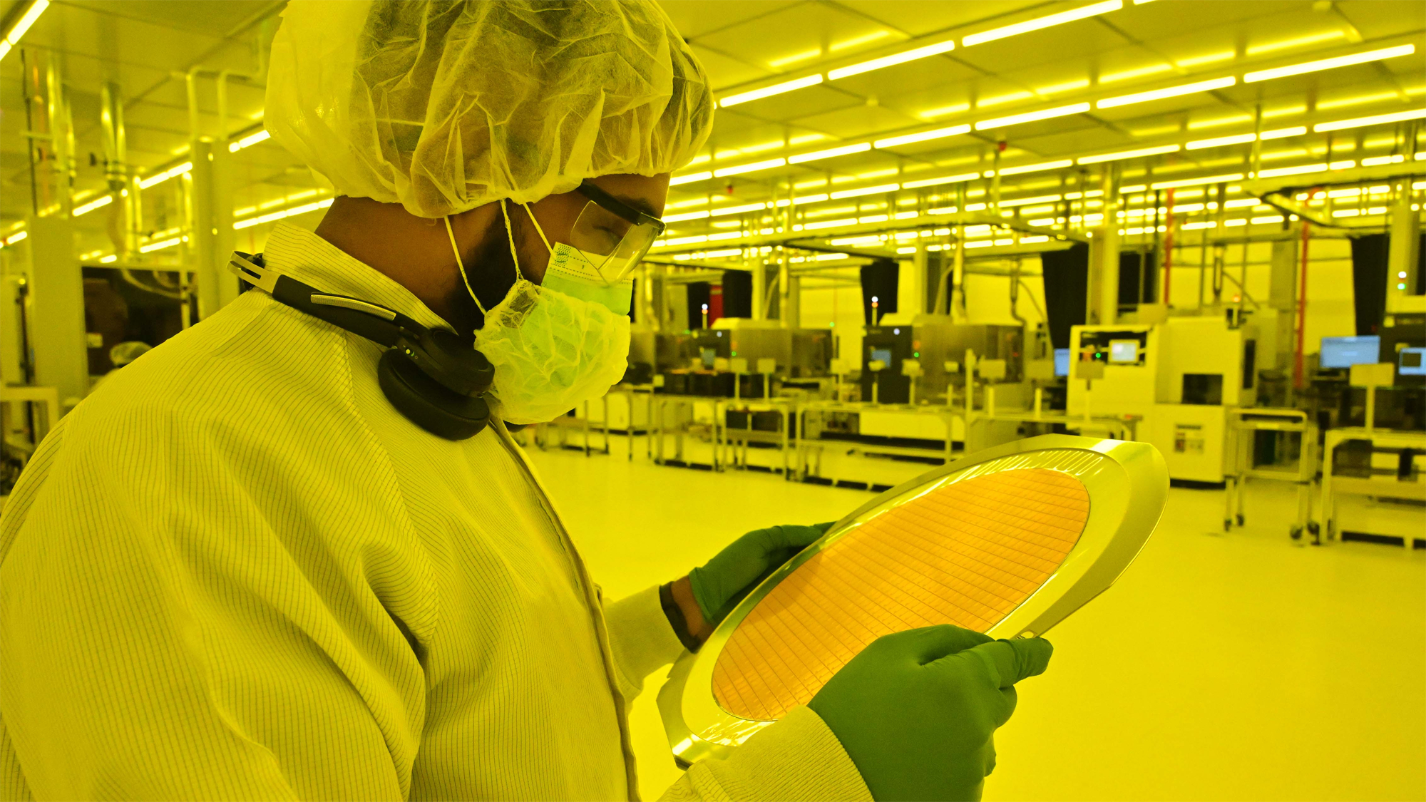
Intel recently invited the global press to see its facilities in Malaysia as part of the Intel Tech Tour, marking the first time the company has opened its packaging facilities in the region to the press. Unlike previous tours that have focused on the actual creation of microprocessors in the company's fabs, Intel's Malaysia tour focused on the next step in production: Packaging, which has become one of the most important battlefields for chip-making supremacy as the industry quickly moves toward chiplet-based architectures to offset the slowing of Moore's Law.
Intel and TSMC are competing furiously to provide the most advanced packaging technologies available, and Intel's Malaysia facilities play a key role in its efforts as it looks to ramp up its Meteor Lake production, a new series of consumer CPUs that employ groundbreaking production techniques. Until now, these facilities have been shrouded in secrecy, and that veil hung thick over our tour. The production capabilities of these facilities and the technology and machines that power them are among some of Intel's most closely guarded secrets. We couldn't bring anything into the production line areas — not even a Fitbit or lip balm — a requirement that security personnel verified with metal detectors before and after we entered the restricted areas.
That level of secrecy is needed to protect Intel's proprietary tech, but it made note-taking a bit tough, especially given the sheer volume of technical information the company shared once we were inside the buildings. We weren't allowed to ask plant personnel questions pertaining to output, yields, or production capacity, or repeat or rephrase any question they refused to answer; violations that we were warned would result in being quickly escorted from the premises. Photos of these restricted areas also weren't allowed, but Intel provided us with hundreds of heavily-screened photos so we can give you a peek behind the curtain. We also have videos of several areas as well.
At its most basic level, chip packaging is the undertaking of processing a finished wafer, cutting it into separate dies, testing and sorting (binning) the chips, connecting them to an underlying substrate that often involves complex connections to other dies, and then placing an integrated heat spreader (IHS) on top to create a fully-functional processor that's ready to head off into distribution channels, then eventually into your PC or other devices. Many of the world's best CPUs are packaged at the facility we visited.
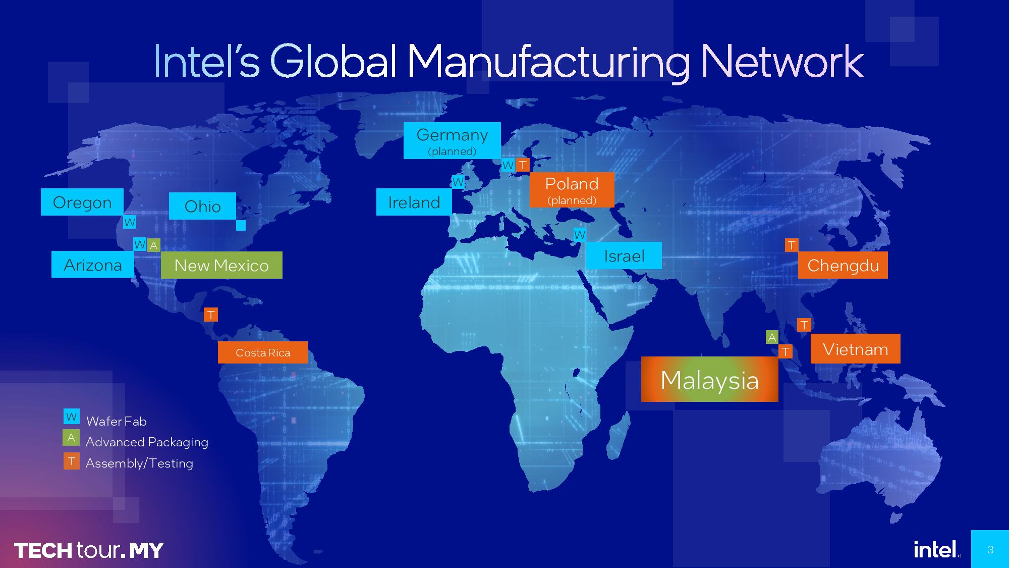
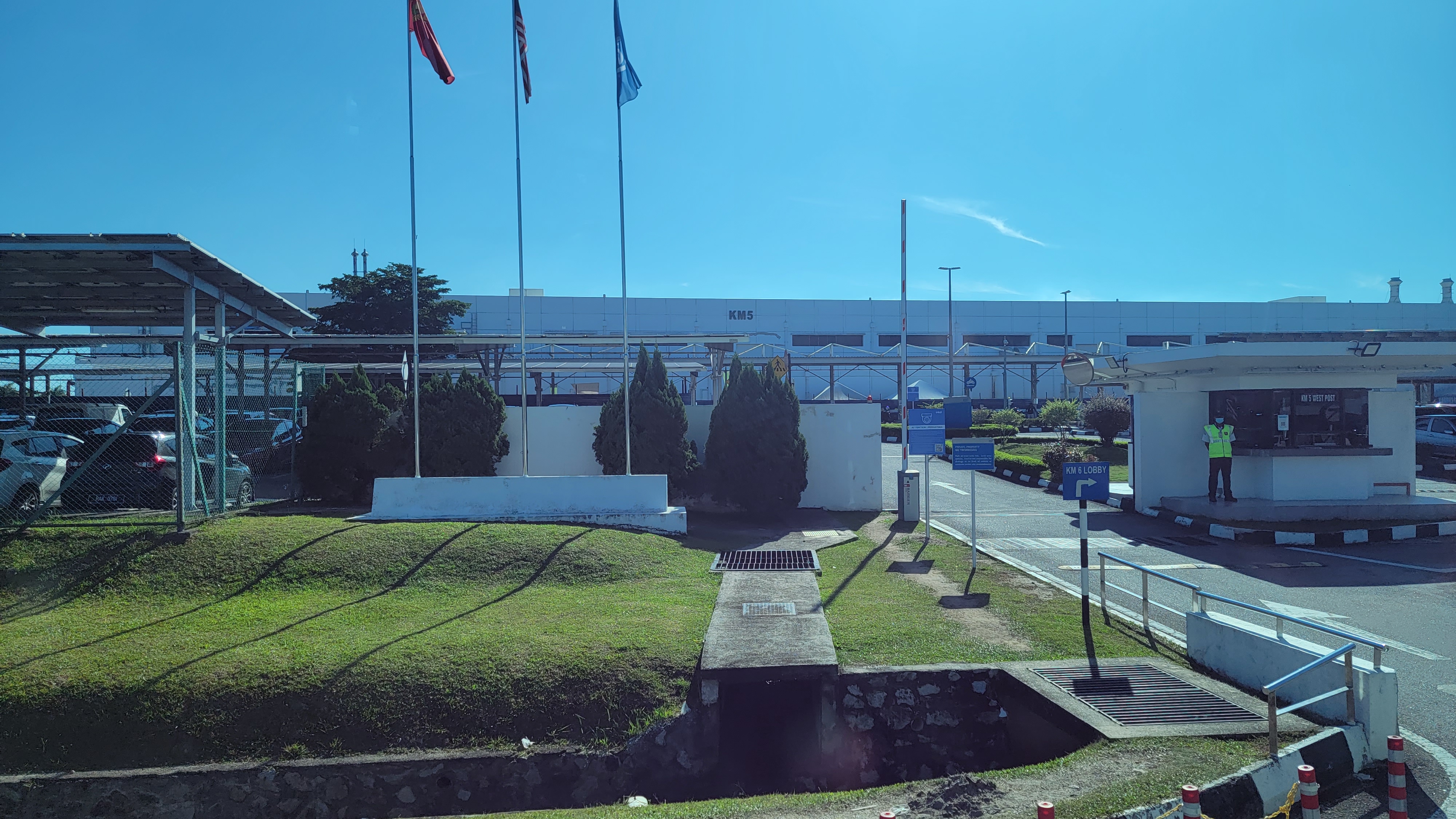


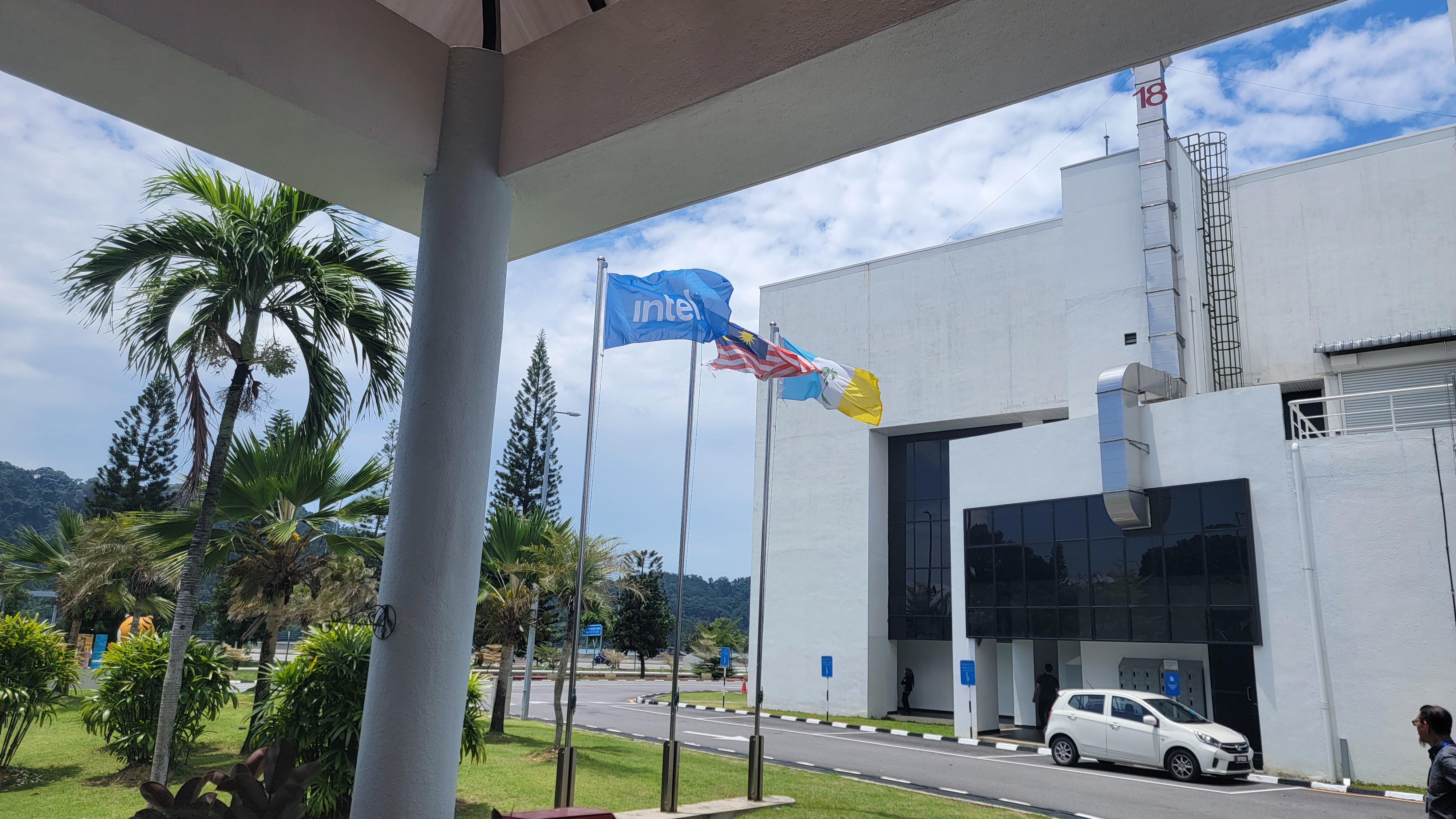
While this process admittedly isn't as exotic as the magical process of actually fabricating a processor by bending light to our will to etch nanometer-scale features, the technological wizardry involved in chip packaging is also mind-bending, especially given the sheer scale of Intel's operation. In total, the company sells nearly a million processors per day, and it leverages a global network of packaging facilities, including facilities in the US, Malaysia, China (Chengdu), and Vietnam, to accomplish that feat.
The map in the album above indicates the locations of Intel's different fab operations, including the wafer fabs (blue), advanced packaging facilities (green), and assembly and test facilities (orange), with Malaysia conducting both advanced packaging and assembly and test. The Malaysian facilities in its Penang and Kulim campuses represent the crown jewels of the company's packaging capabilities. Although those fabs are listed as advanced packaging capable due to their EMIB packaging capabilities, they currently don't do Foveros packaging for Meteor Lake — that step is done first in Rio Rancho, New Mexico. The final process of employing EMIB packaging in the final chip is done in Malaysia. Intel's ongoing expansion in Penang will soon add the ability to do Foveros packaging in Malaysia.
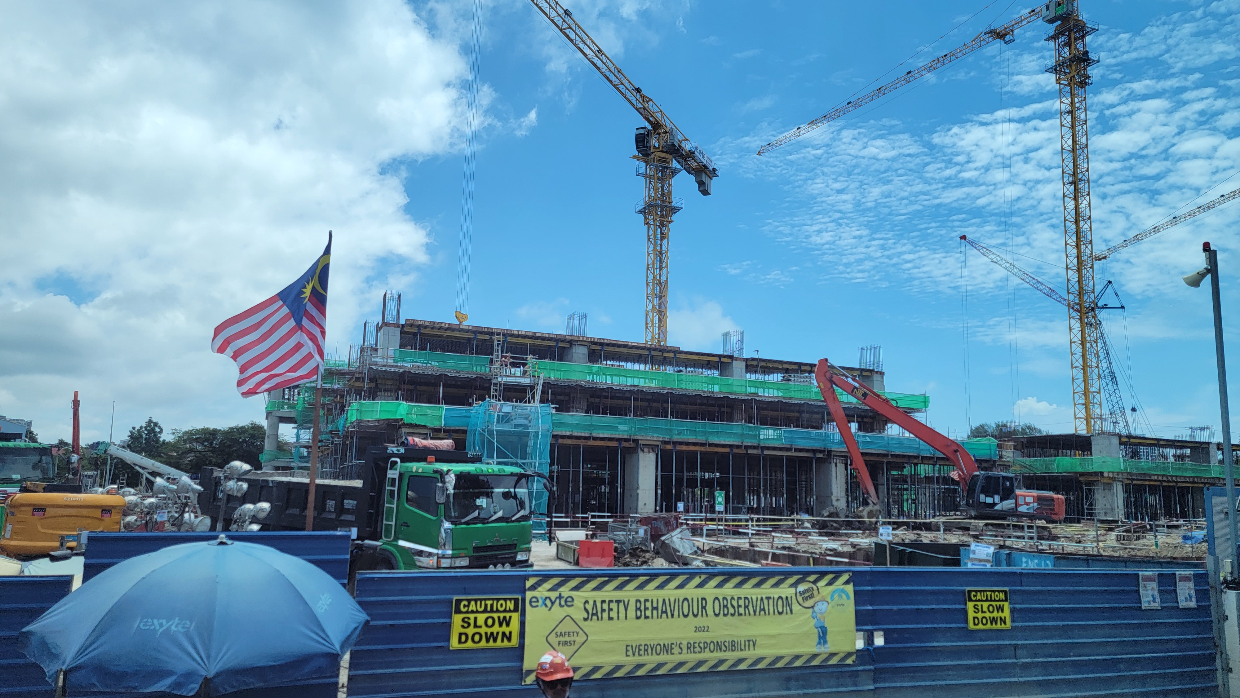
Intel has held several tours of its factories in recent times, and an assortment of construction cranes piercing the sky always makes it easy to spot the company's campuses from far away. Intel's Malaysian campuses are no exception.
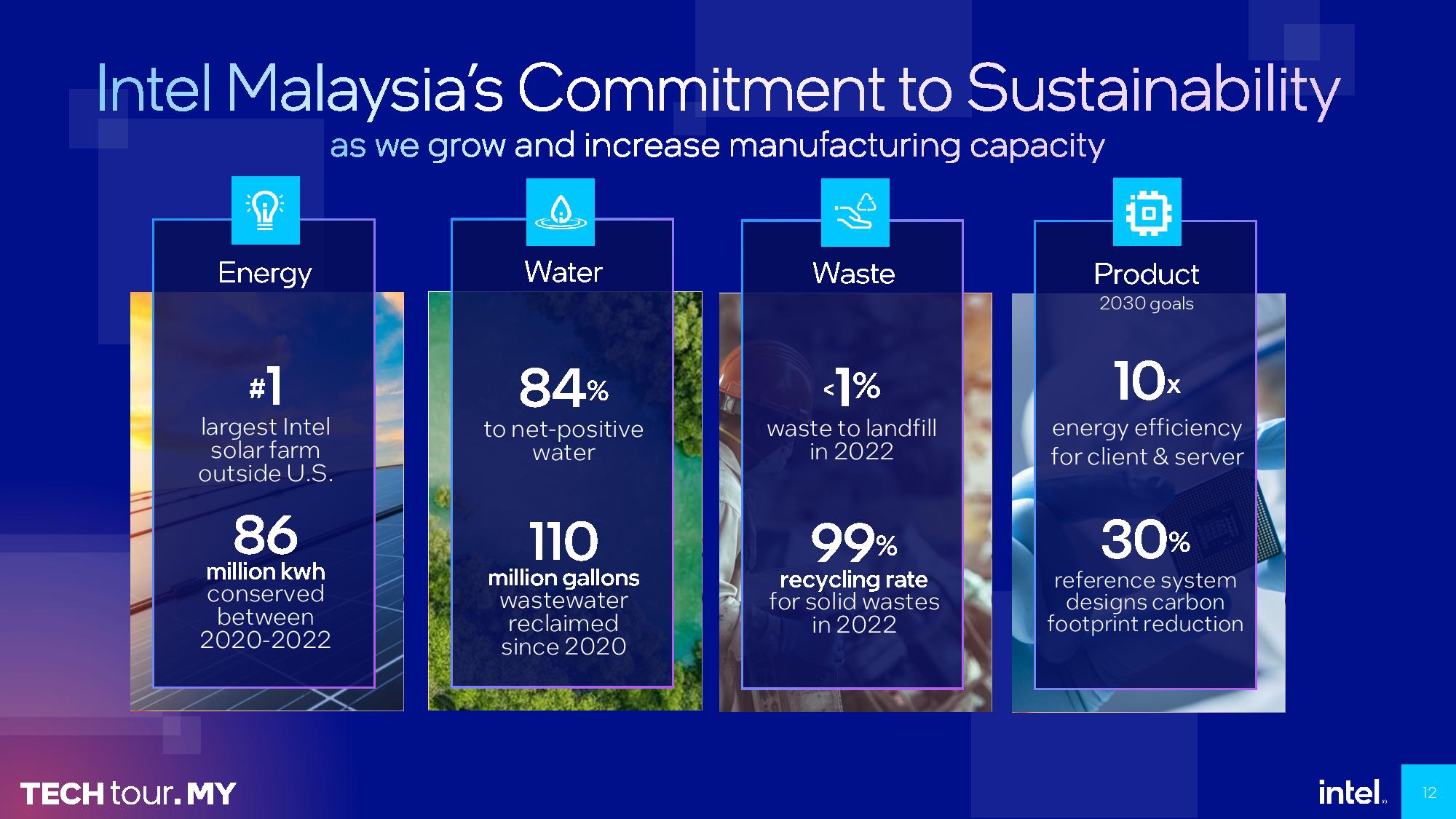
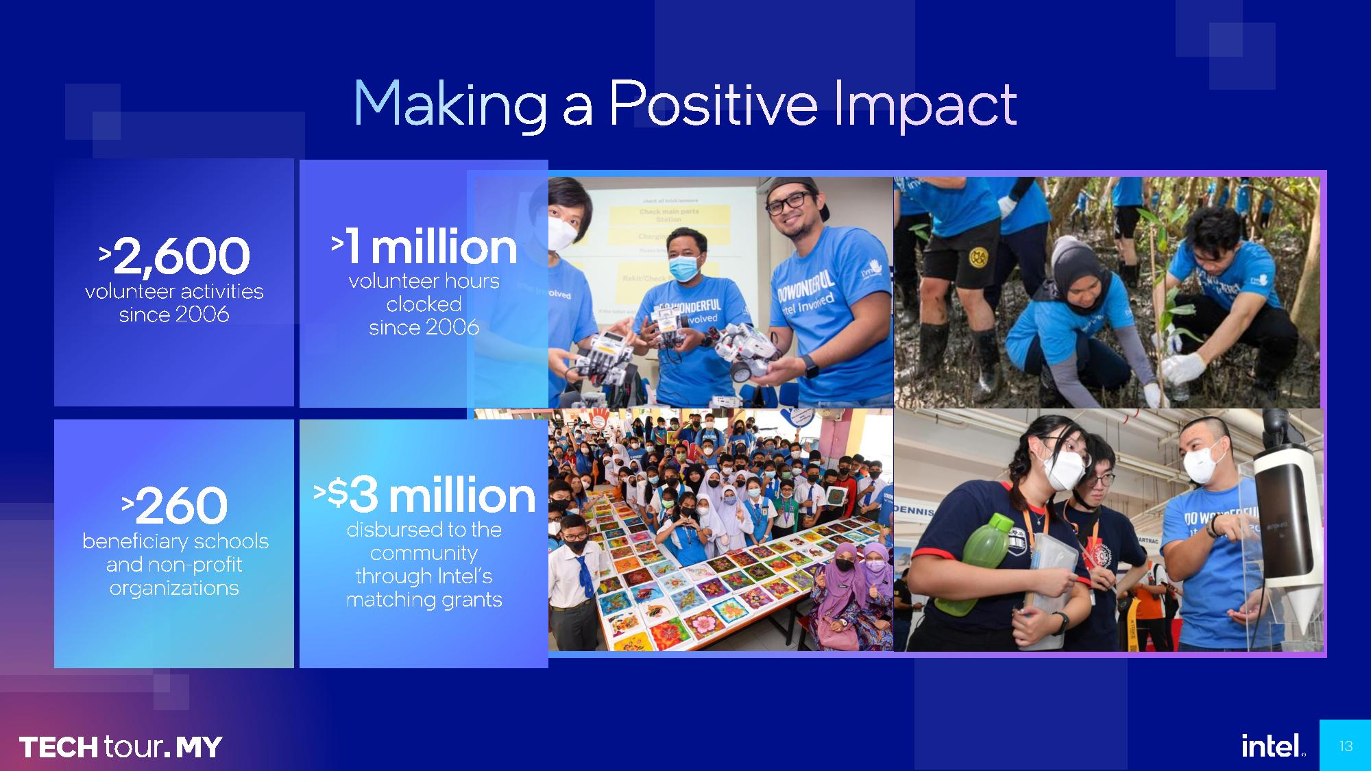
These cranes aren't needed for the day-to-day operation of the plants. Instead, they're part of Intel's rapid expansion as it races to build out both the fab and packaging capacity to satisfy the at-times insatiable demand for semiconductors while working to reach its goal of delivering five new process nodes in four years. The company is clearly aligned on this audacious goal; 'Five nodes in four years' is a pervasive mantra repeated by everyone from the executives and marketing leads down to the personnel on the factory floor.
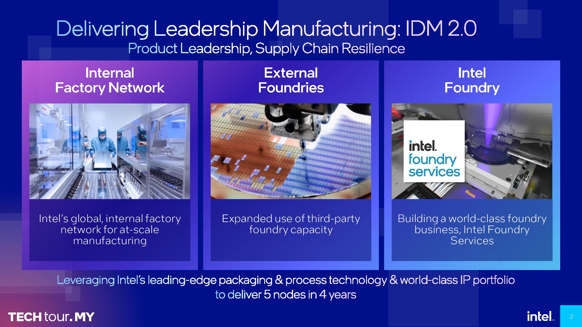
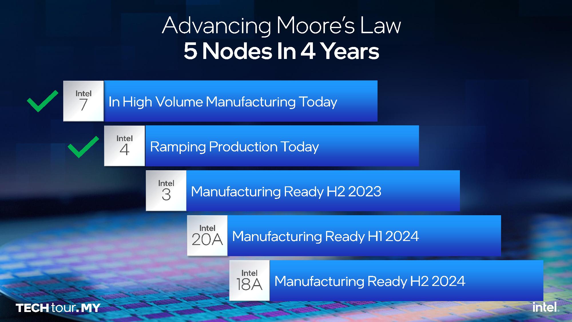
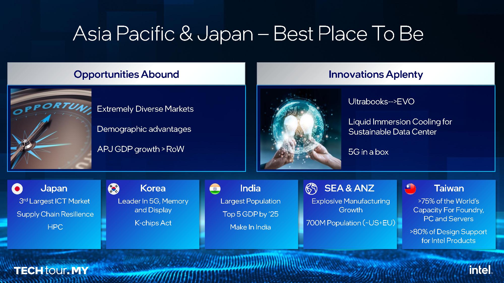
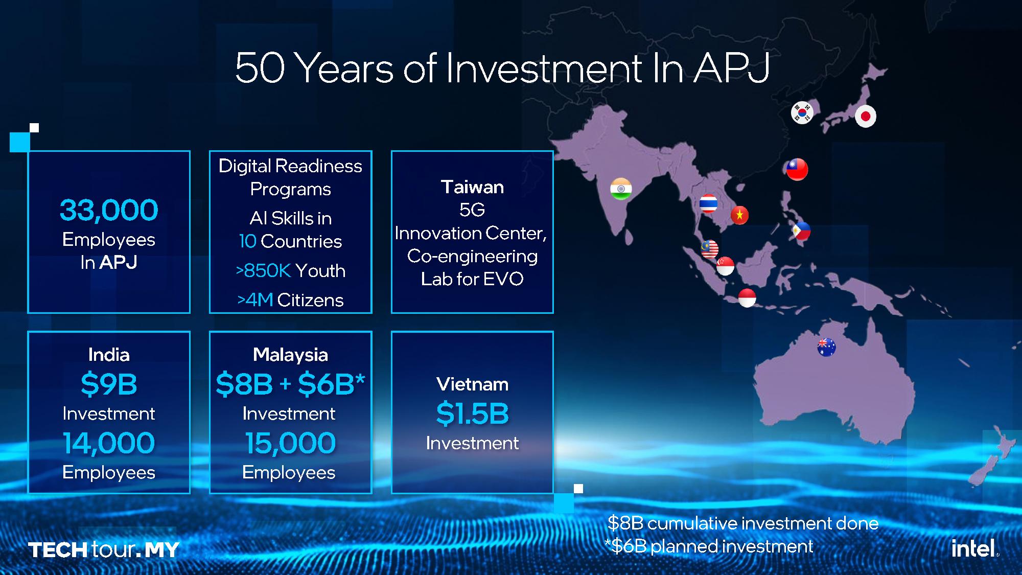
Intel already has two phases of that goal under its belt with the Intel 7 and Intel 4 nodes, and says it remains on schedule to achieve the other three milestones with Intel 3, 20A, and 18A. If successful, those advanced nodes will grant Intel the lead over TSMC for the first time in years, fueling not only Intel's own products but also helping the company deliver on its IDM 2.0 objective that will find the company fabbing and packaging chips for external customers for the first time through its Intel Foundry Services (IFS) unit.
Intel's calculated IDM 2.0 gamble requires rapid production expansion, some of it partially funded by the US government via the $52 billion CHIPS Act as the country seeks to shore up its indigenous production. However, some of the success of Intel's IFS will rely upon its packaging abilities, with Amazon Web Services being among the first customers for its chip packaging services.
Intel also needs to boost its own advanced packaging production capacity as it ramps up the production of its Meteor Lake chips, the first high-volume chips to employ the company's Foveros and EMIB packaging technologies, and Malaysia plays a key role.
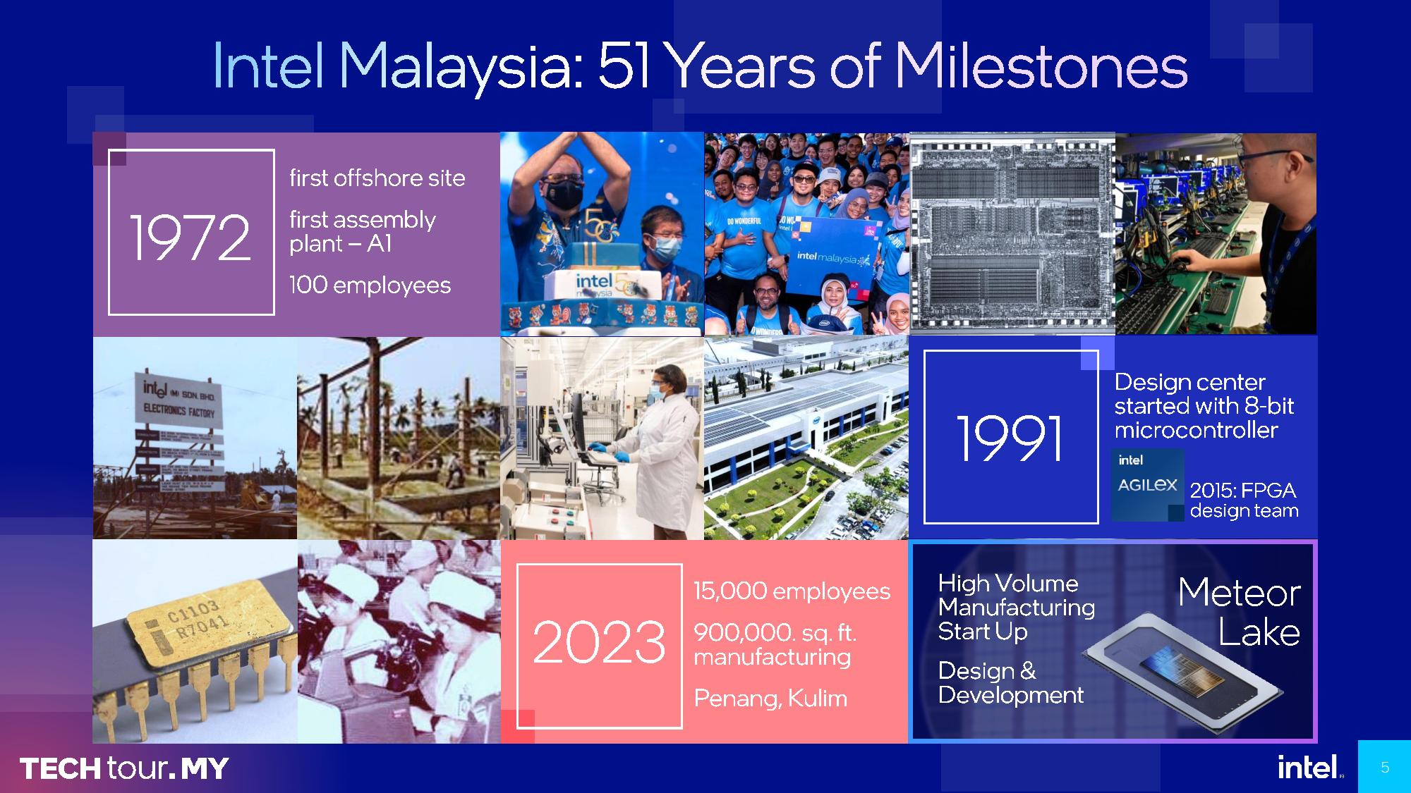
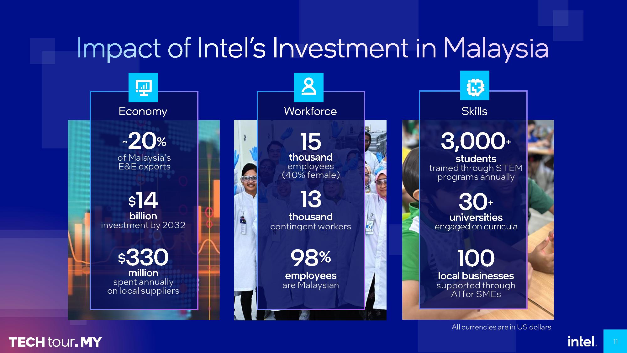
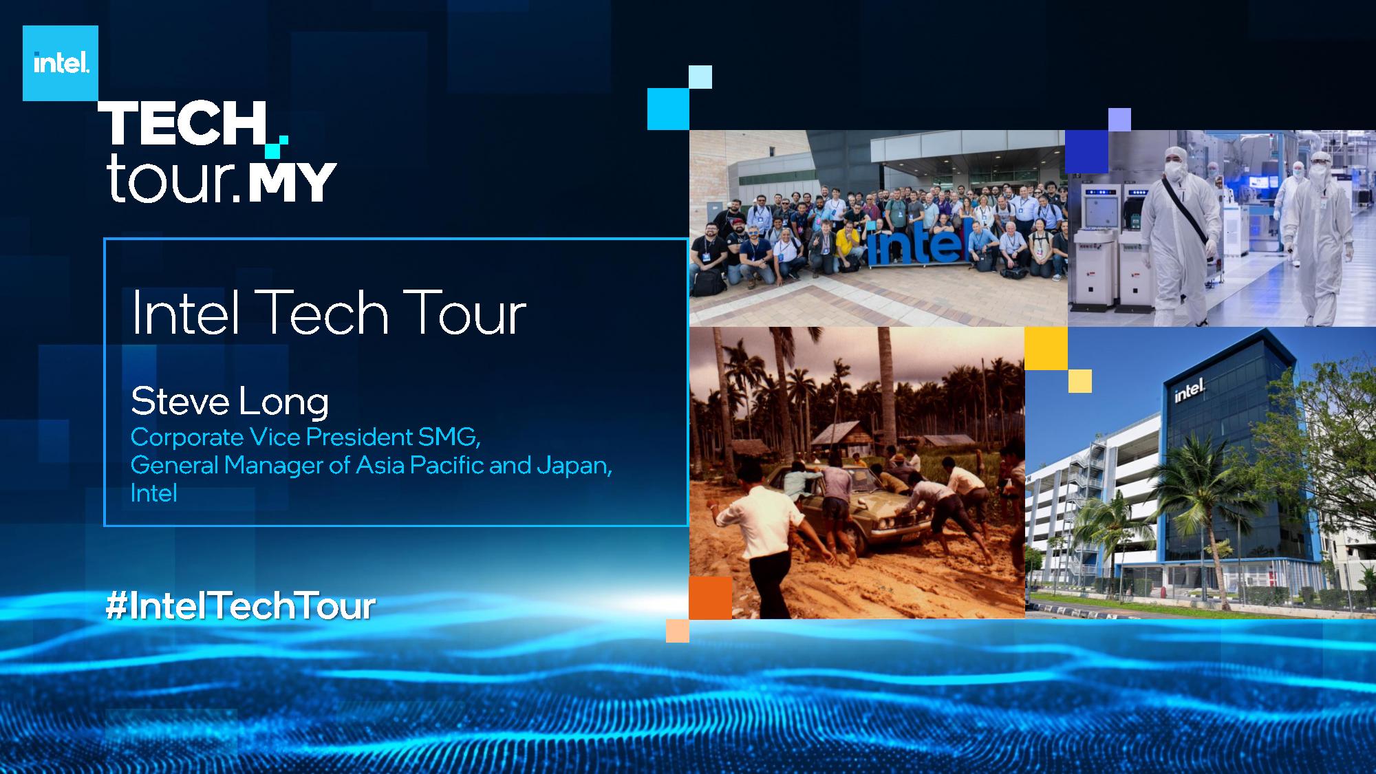
Intel began production in Malaysia, its first off-shore site, 50 years ago with 100 employees at its A1 factory. The Malaysian facilities stand prominent in Intel's history; in the famous image above, we can see Penang employees pushing Intel co-founder Andy Grove's vehicle from the mud after a monsoon hit in 1972. Intel's operations in Malaysia have expanded rapidly from those humble beginnings; Intel now employs 15,000 employees in Penang and Kulim and has 900,000 square feet of manufacturing space. Intel says the sites have processed 1.2 billion chips in the last ten years and have 'sorted' (binned) over 500 million die.
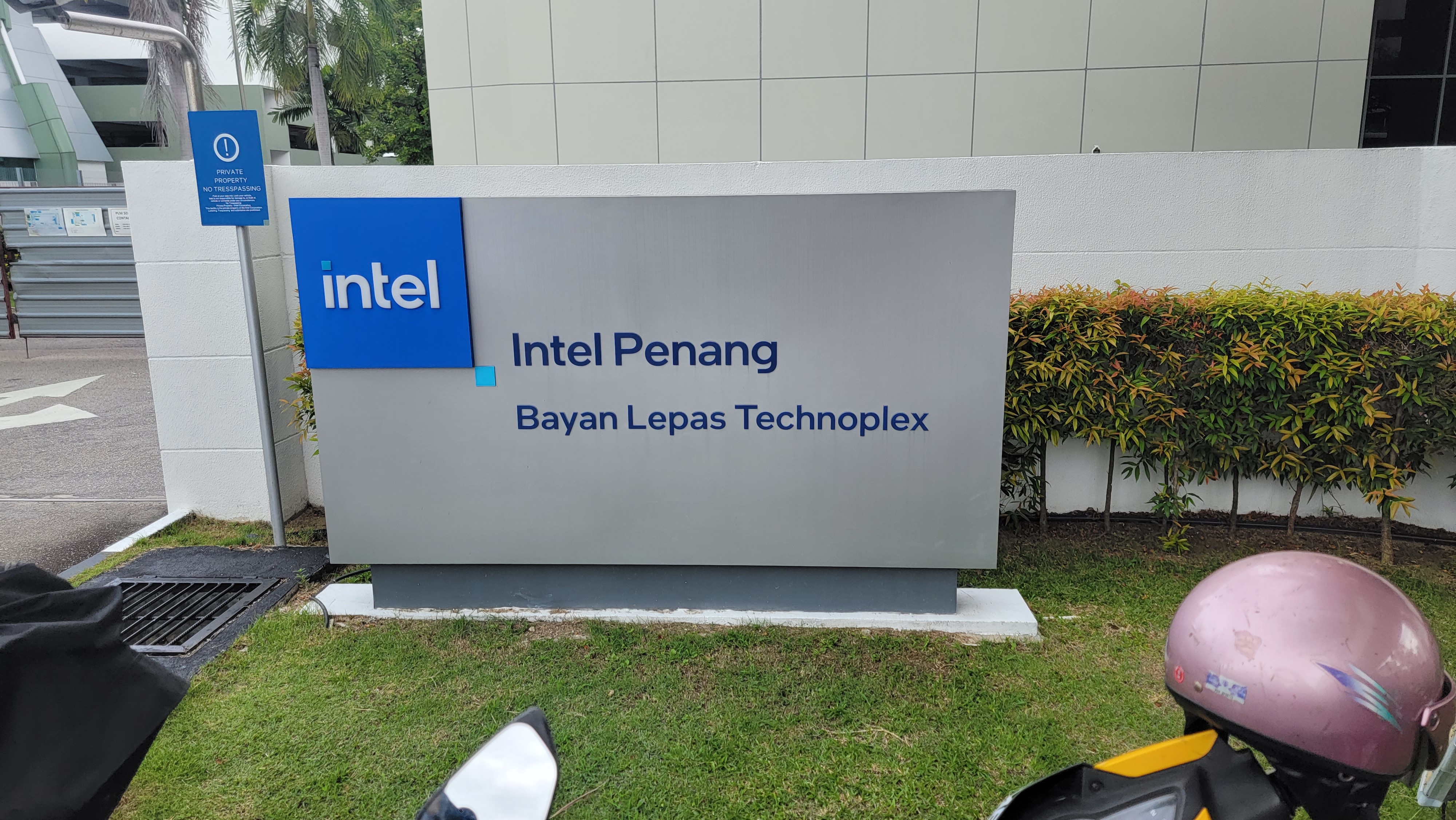
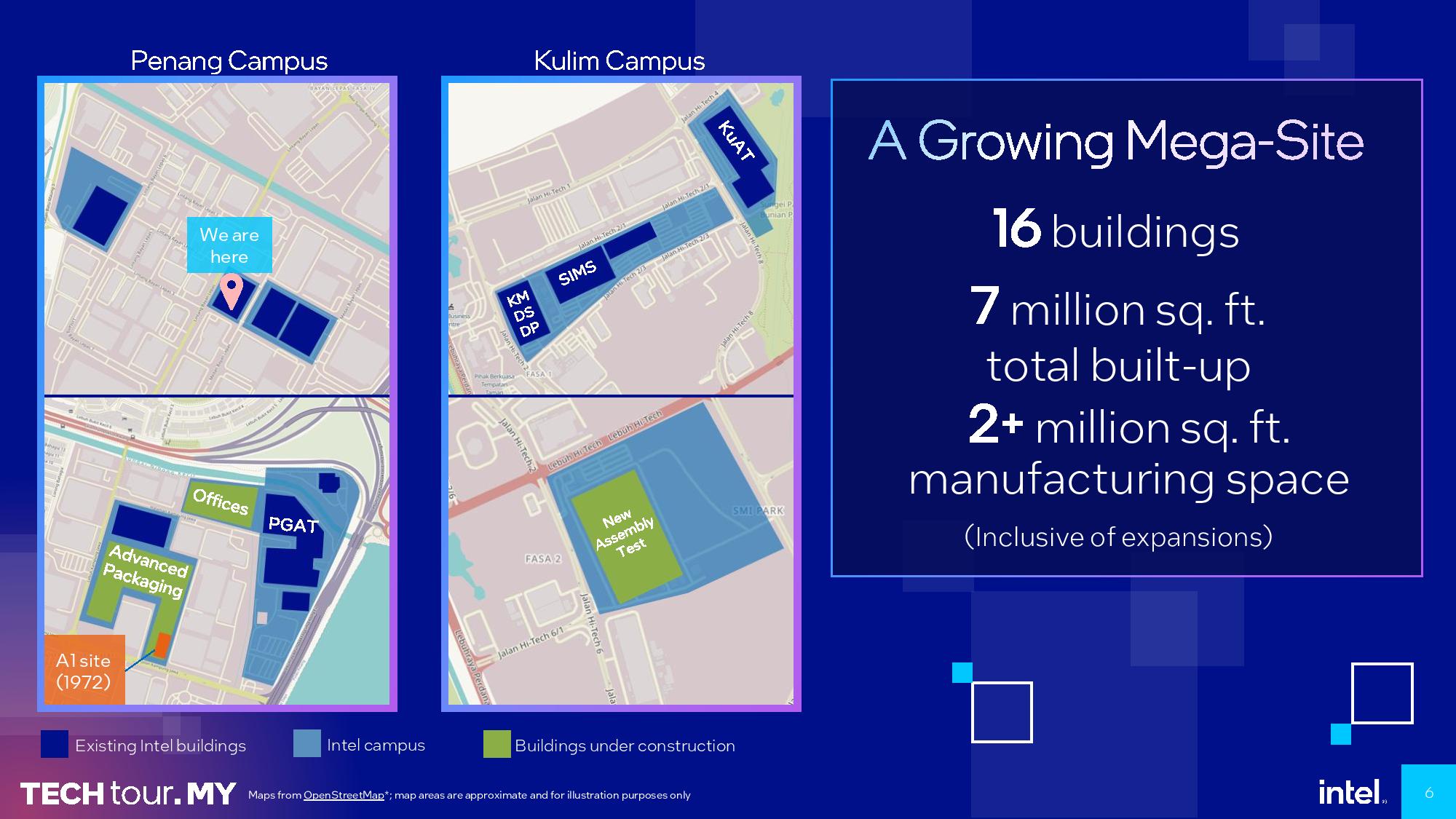
Intel's current expansions will boost its Malaysian operations to 2 million square feet of manufacturing space and 7 million total square feet dedicated to operations, all spread over 16 buildings. Part of the Meteor Lake production will take place at the company's new Pelican facility that it's building at its Penang Malaysia campus for use in the 2025-2026 timeframe. Intel is also building a new Falcon facility at its Kulim site, which we also visited. Both of those come on the heels of other recent expansions that have significantly increased capacity at both locations.
The Chip Production Process Flow
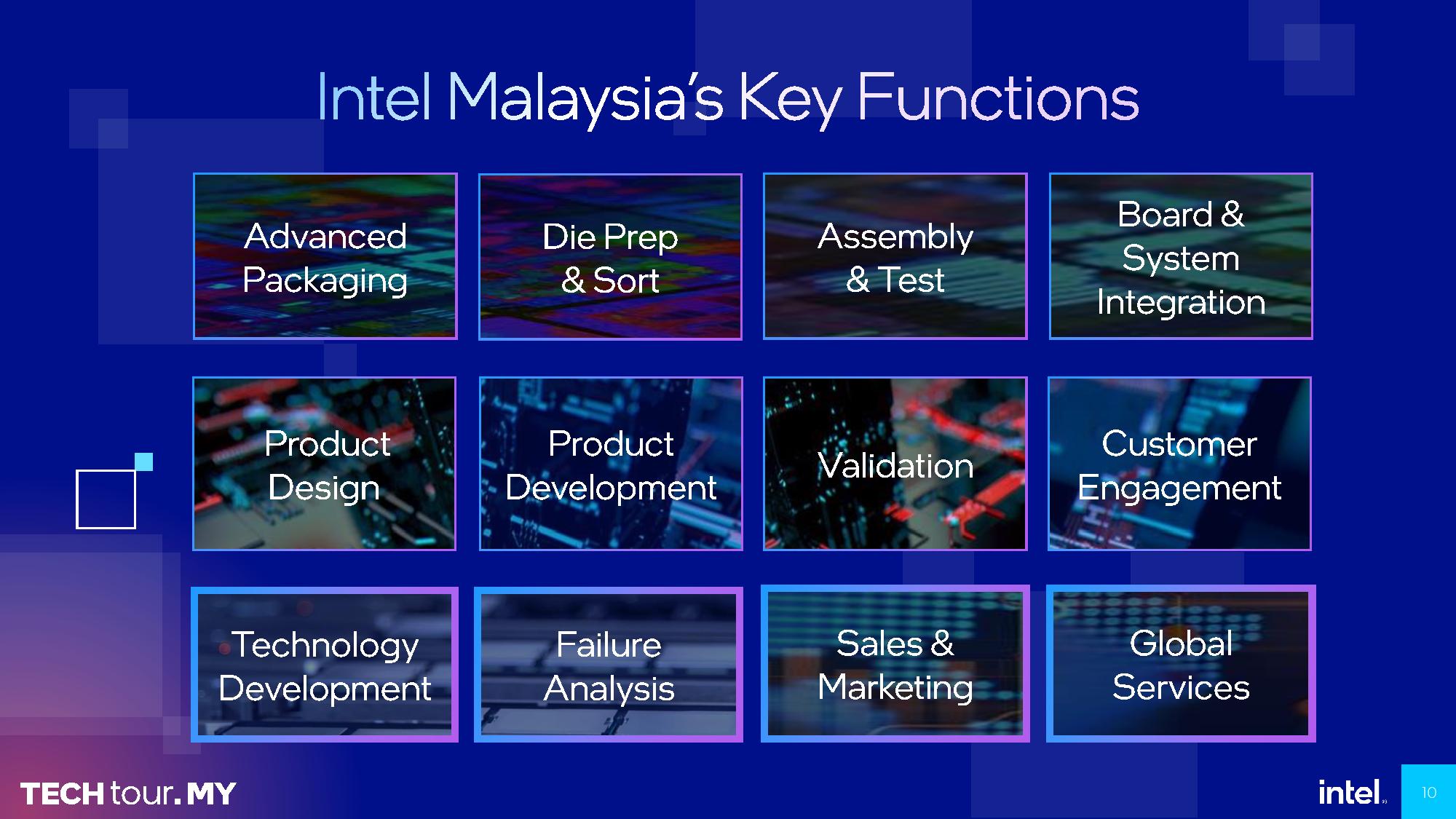
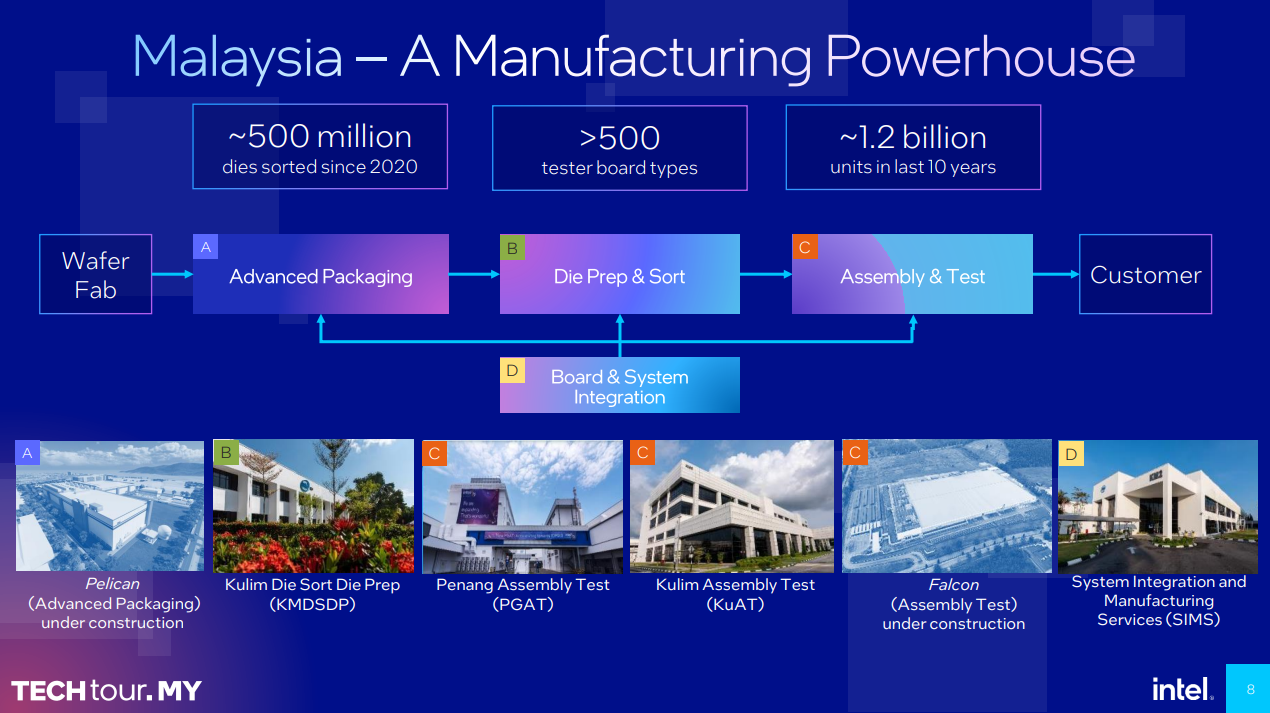
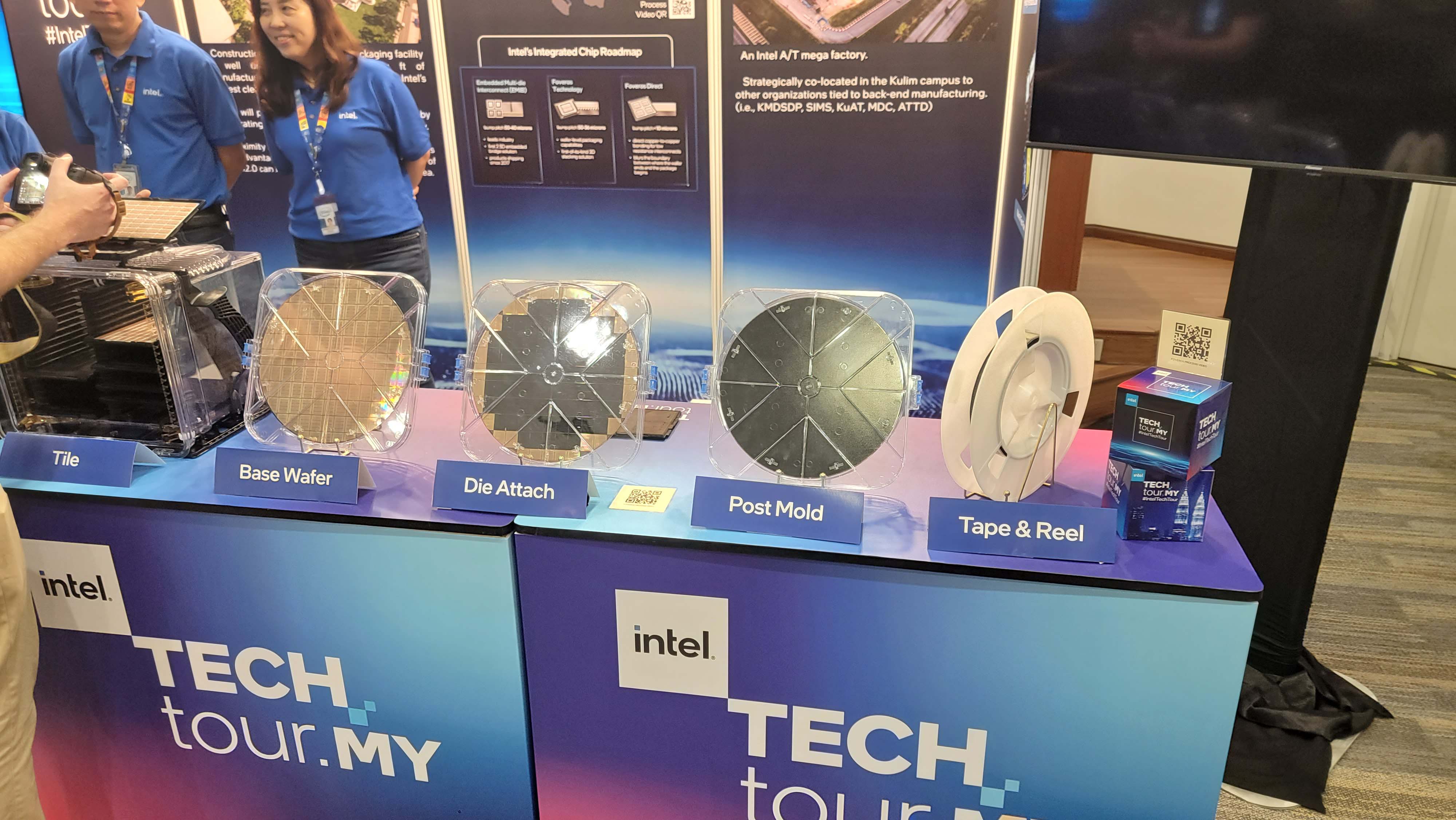
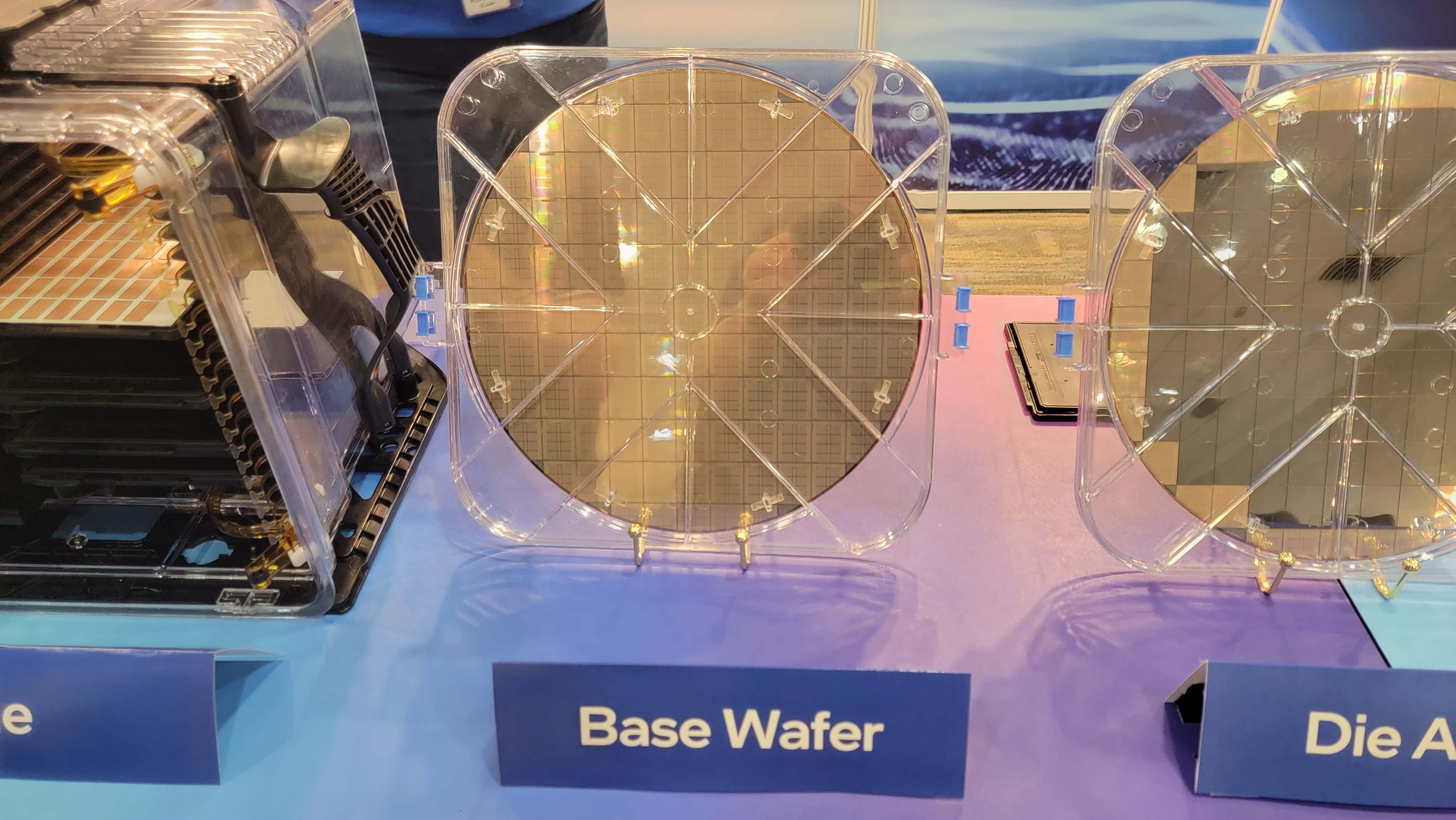
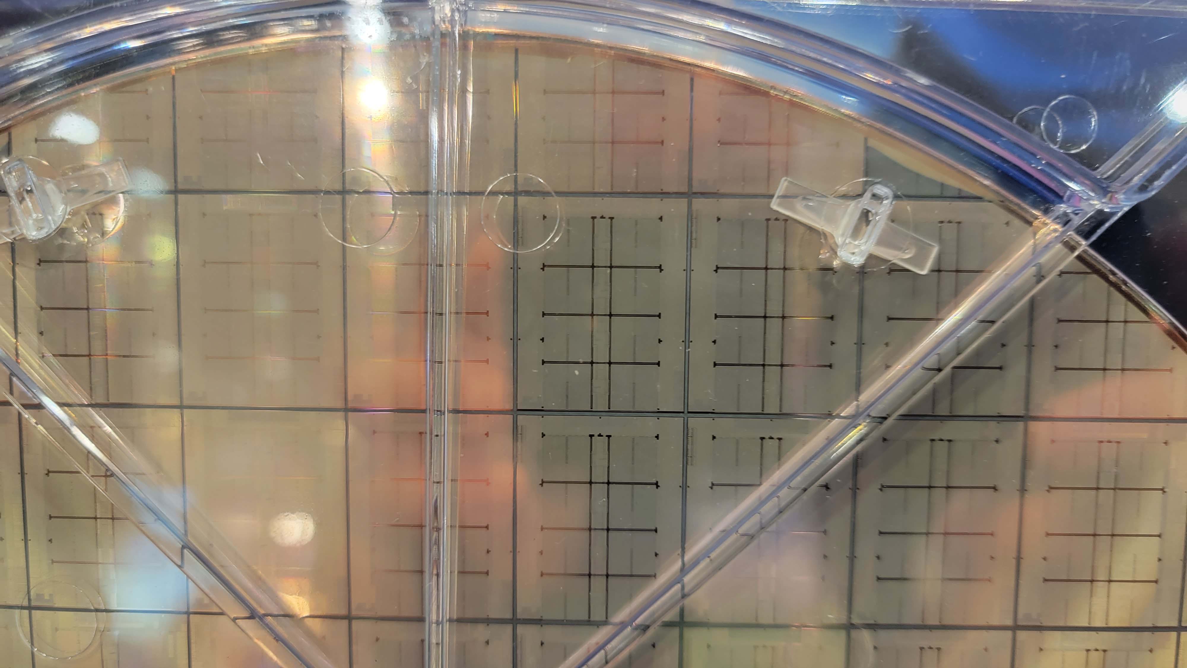
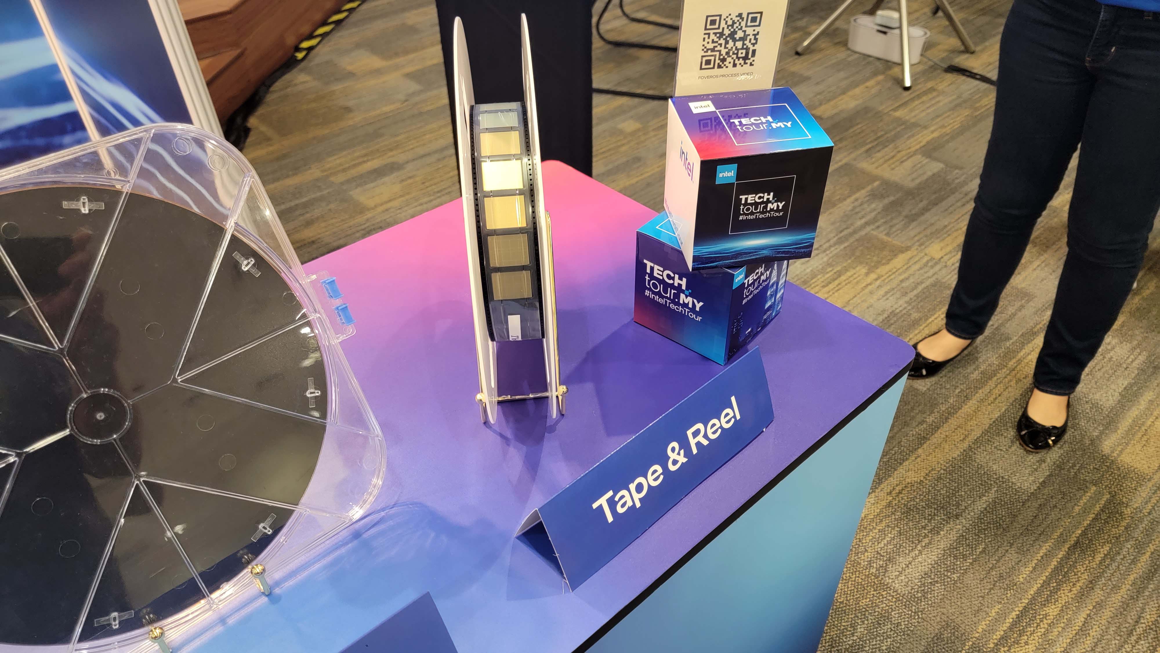
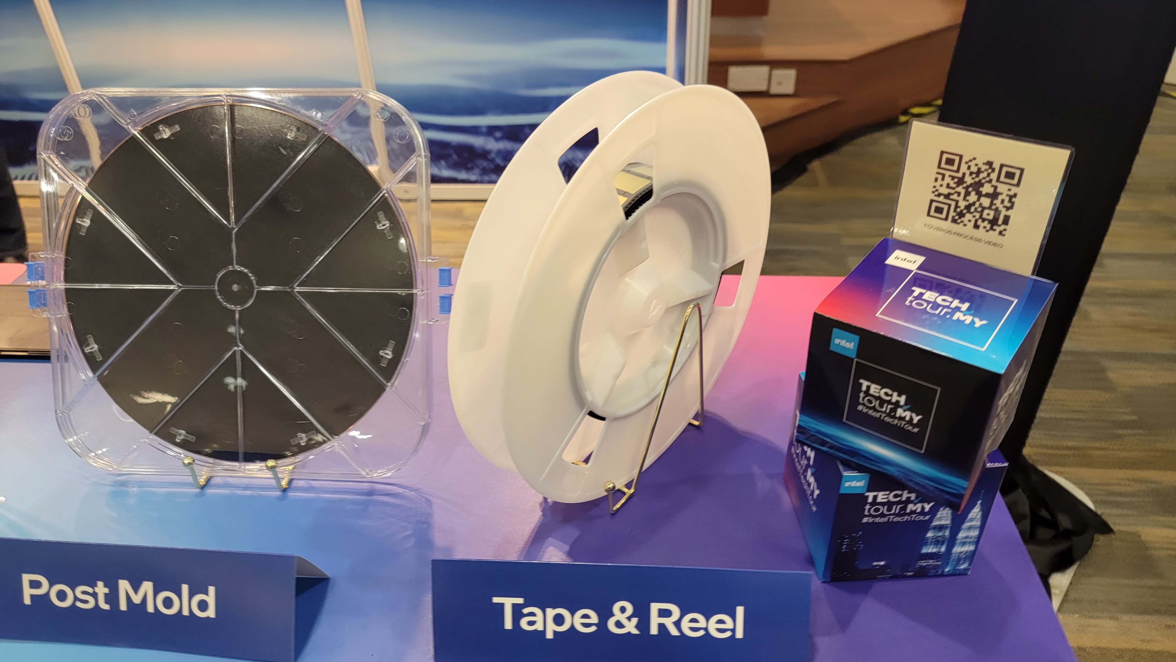
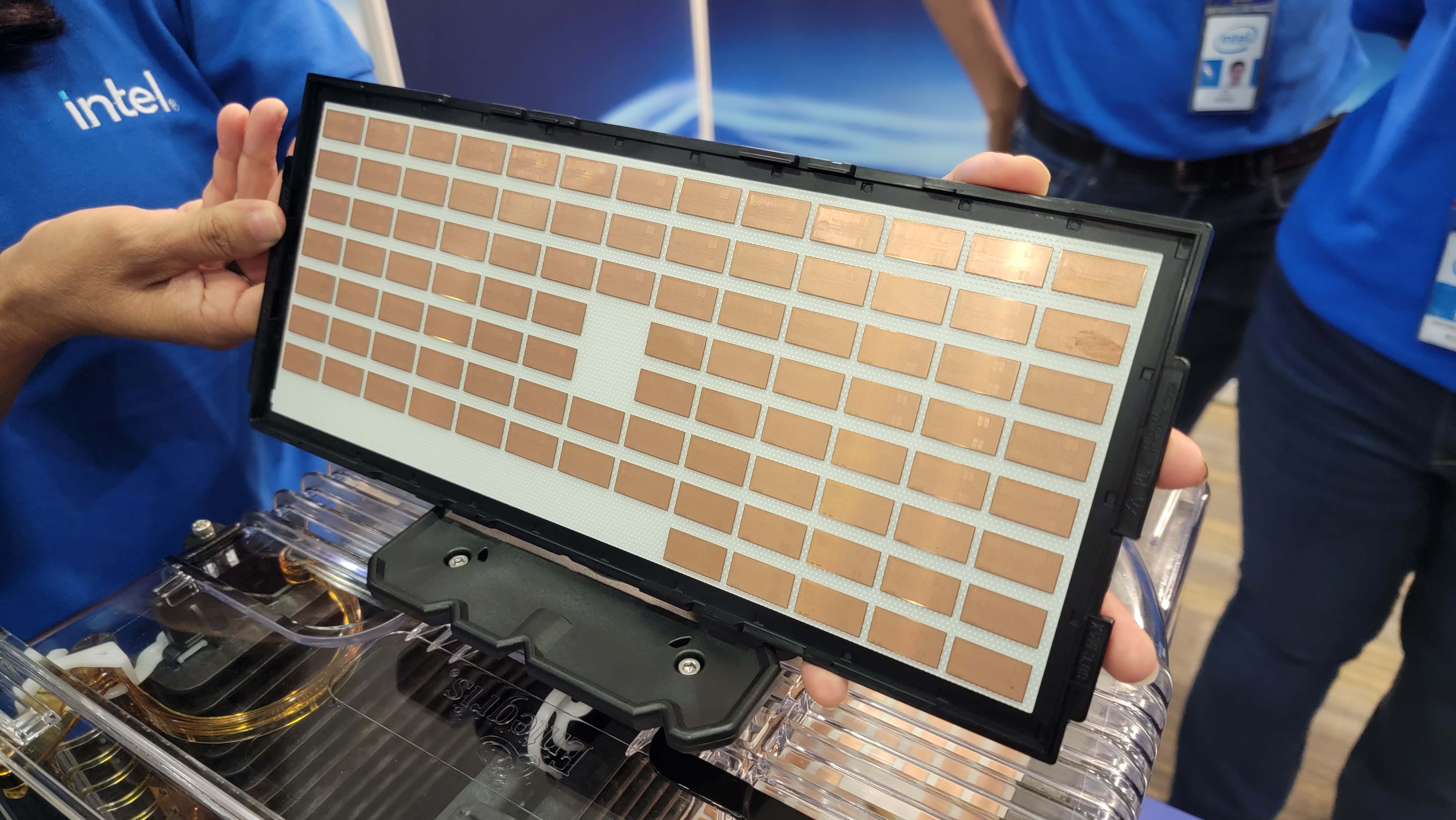
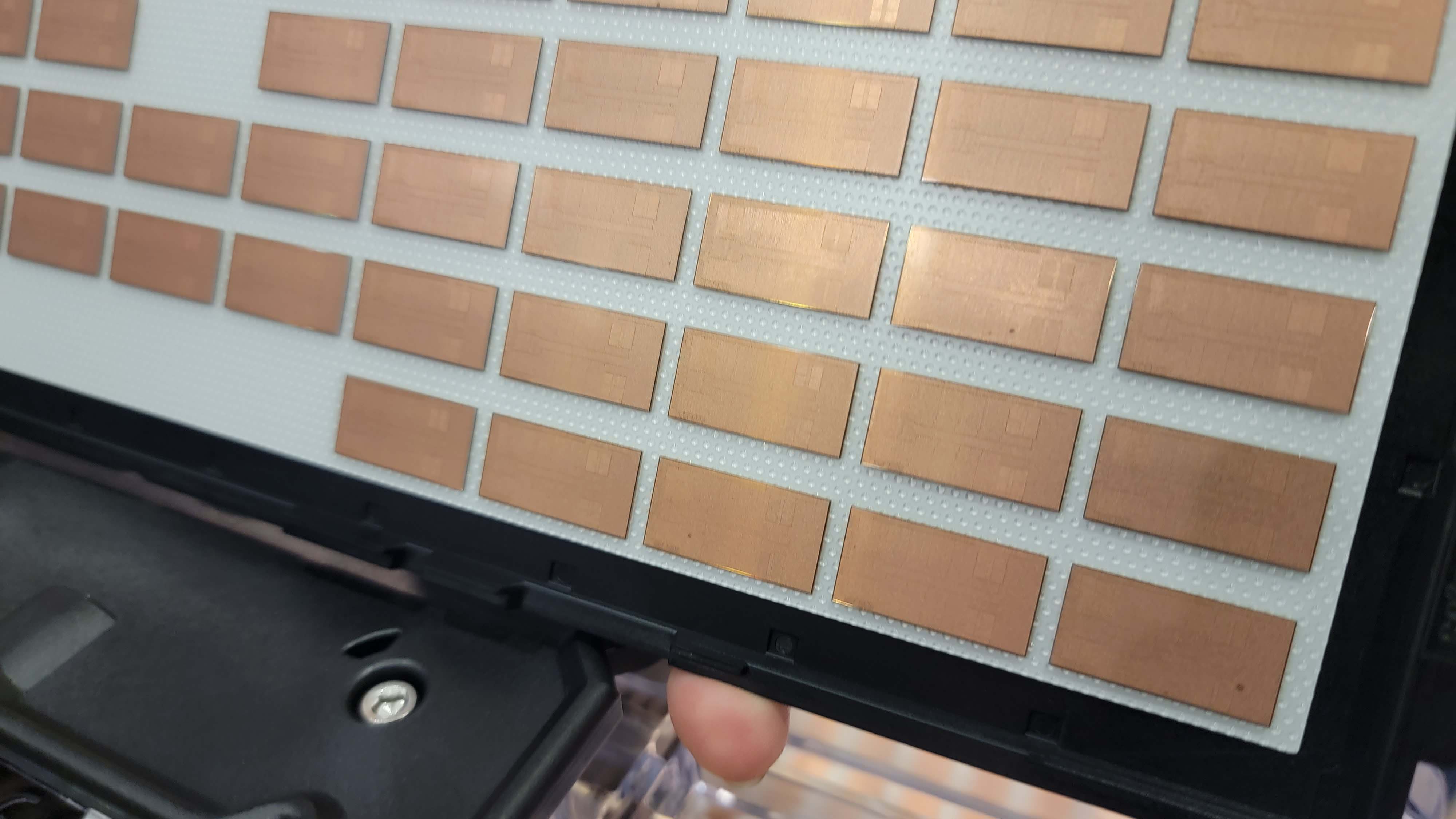
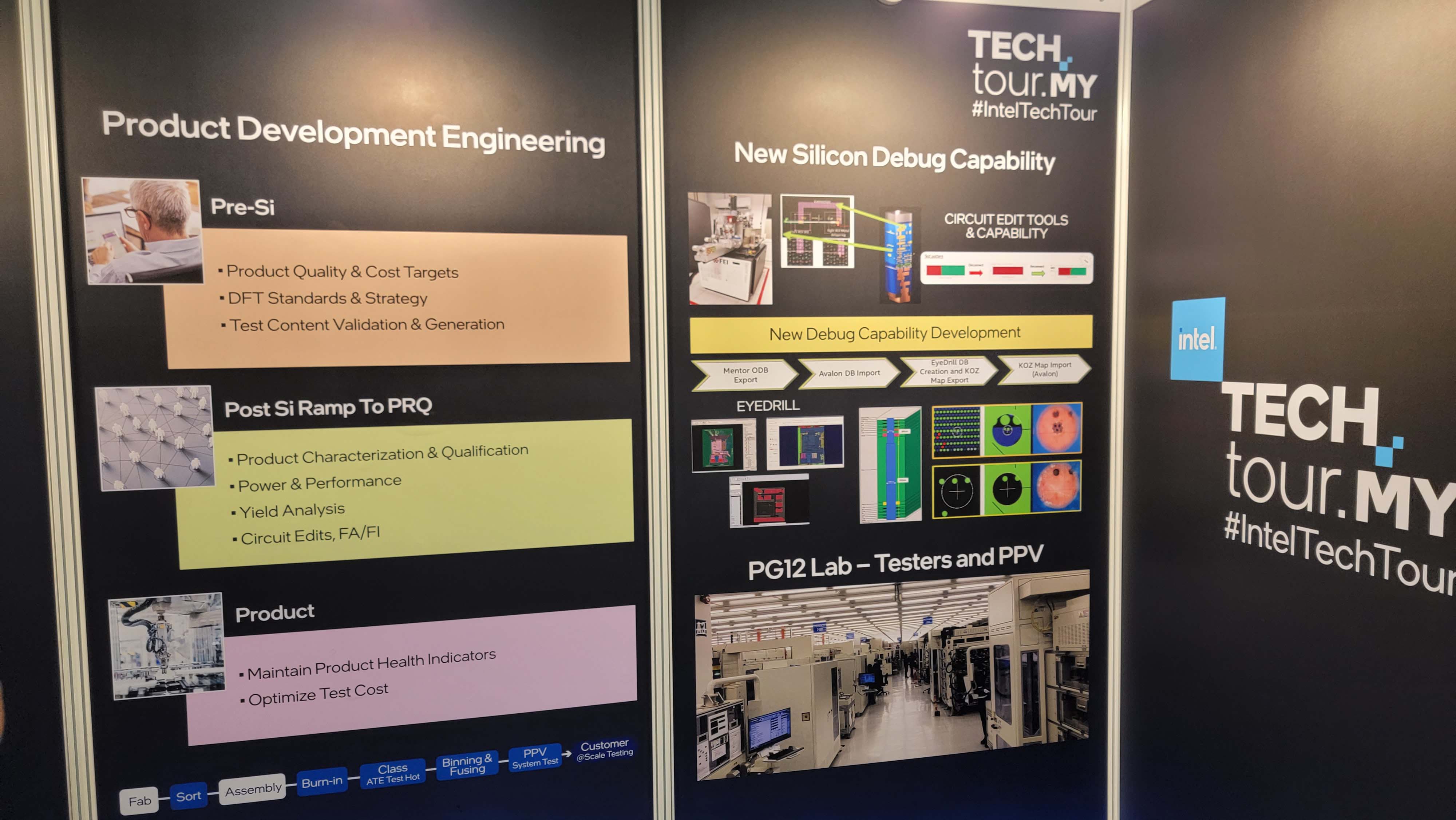
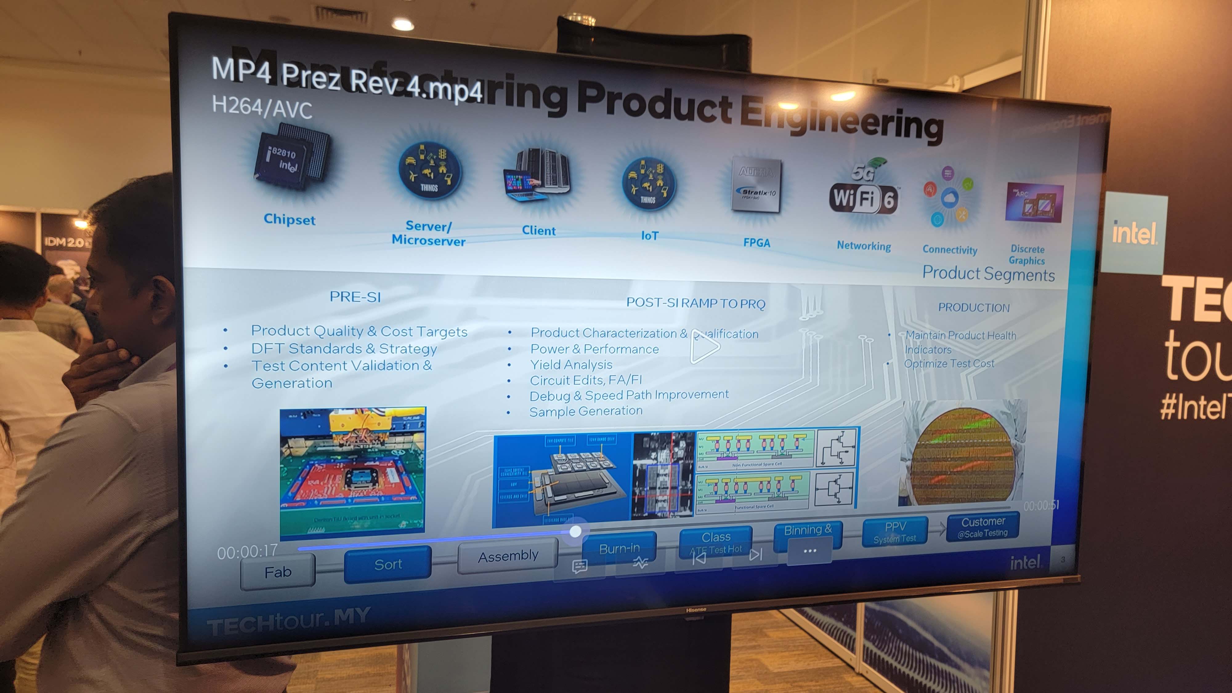
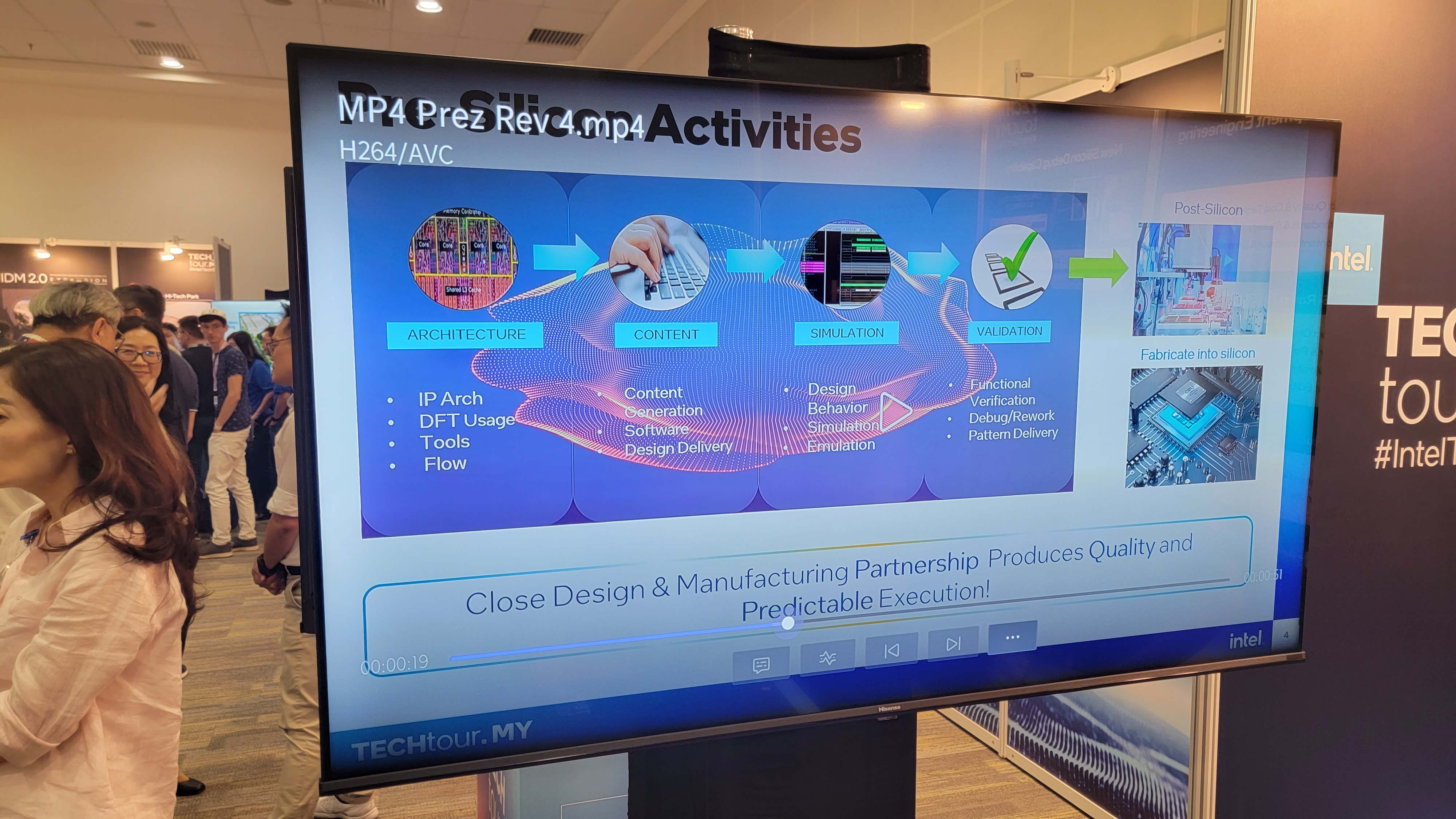
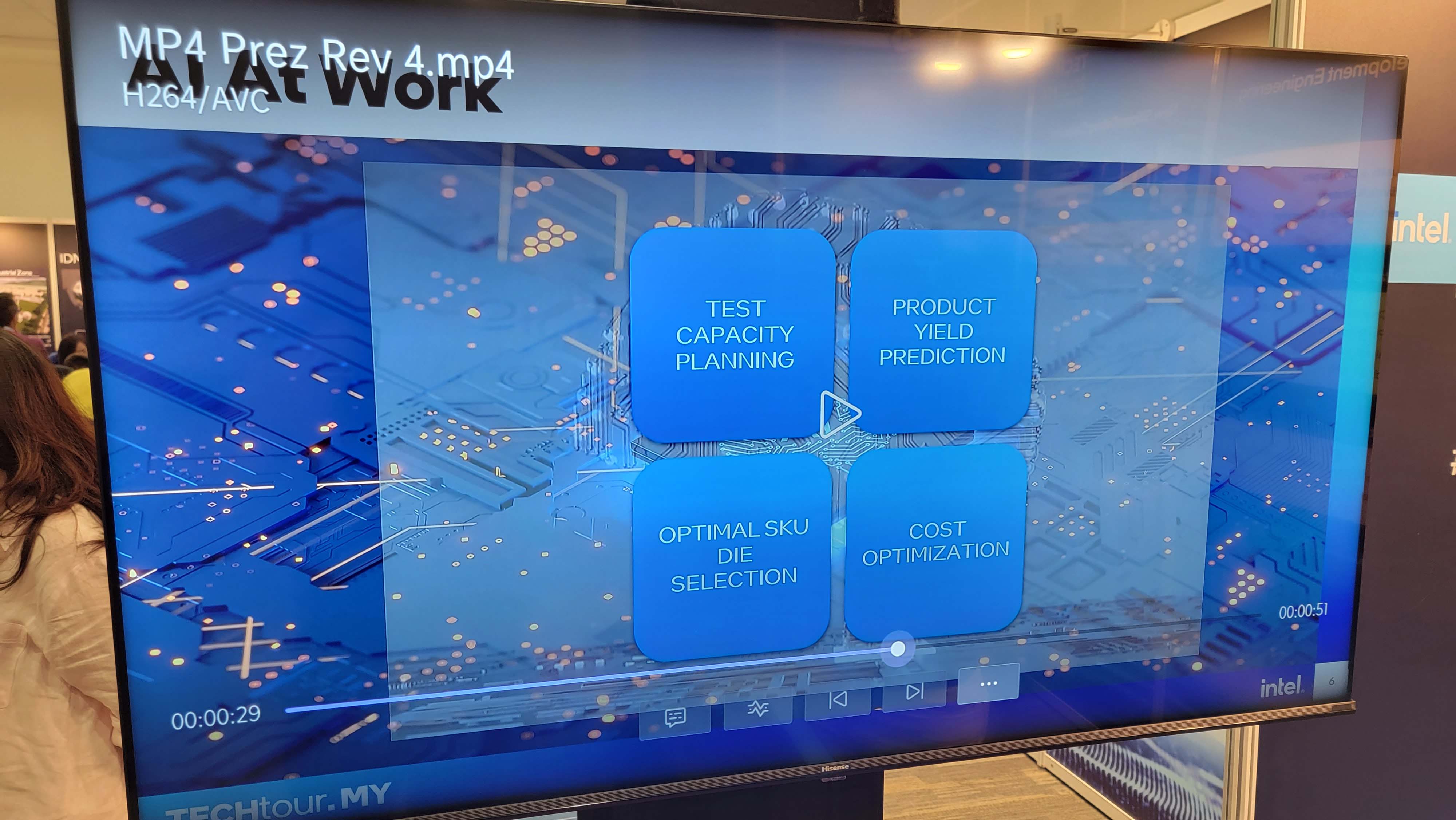
Intel's production flow at its Malaysian facilities consists of multiple steps, with wafers first arriving at the Kulim Die Sort and Die Preparation (KMDSDP) facility to separate individual die from the wafer, which includes grinding, laser scribing and wafer slicing (cutting the die from the wafer). The chips are then sorted, which is the process of testing them for defects before placing the dies on reels (images 5 and 6 in the above album) before sending them to the production phase.
Get Tom's Hardware's best news and in-depth reviews, straight to your inbox.
The reels with the separated dies are then transferred to the Penang Assembly and Test (PGAT) facility, where the die progresses through more production steps that include attaching the die to a PCB, adding epoxy, and attaching the integrated heat spreader (IHS), among other tasks.
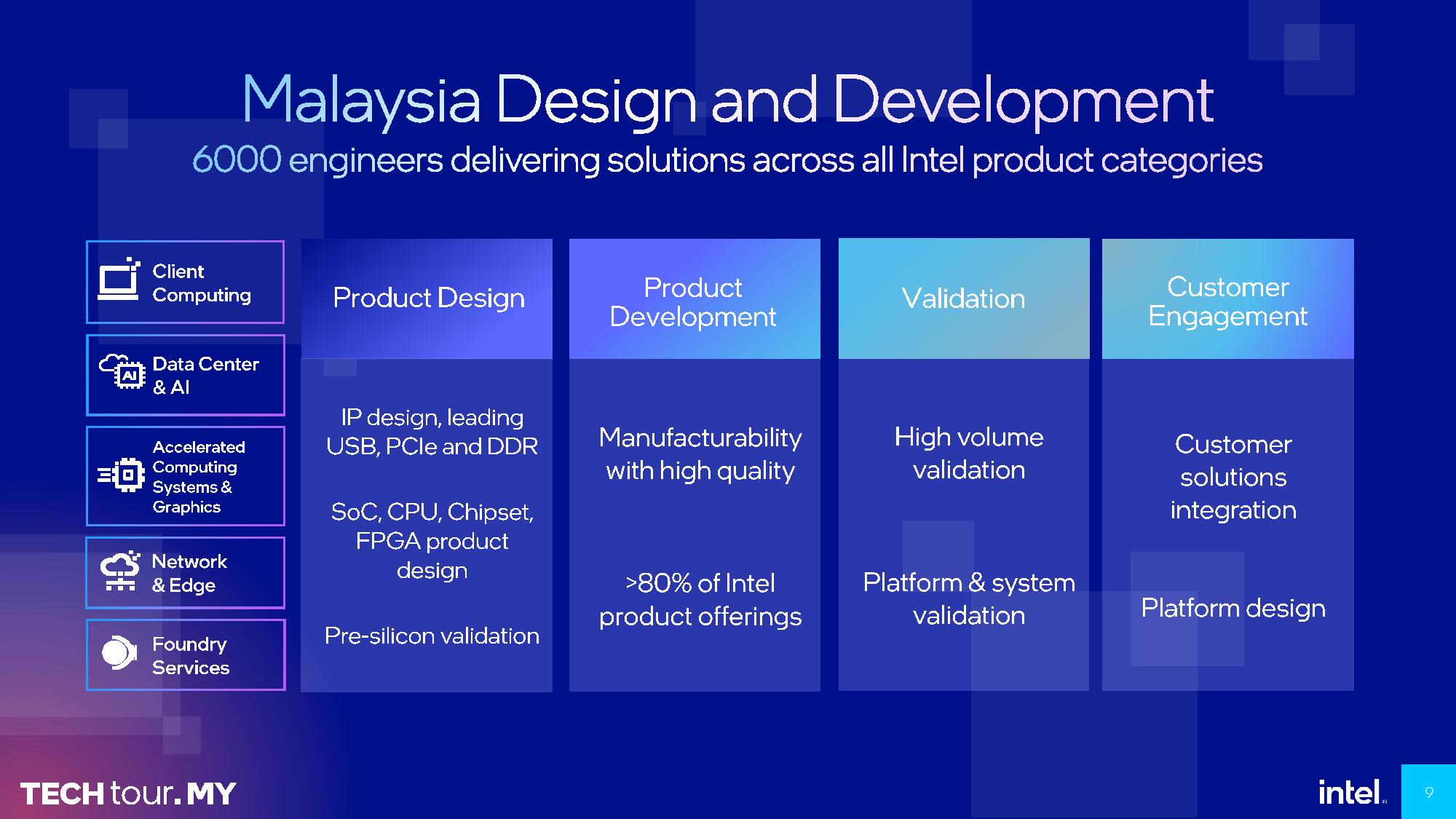
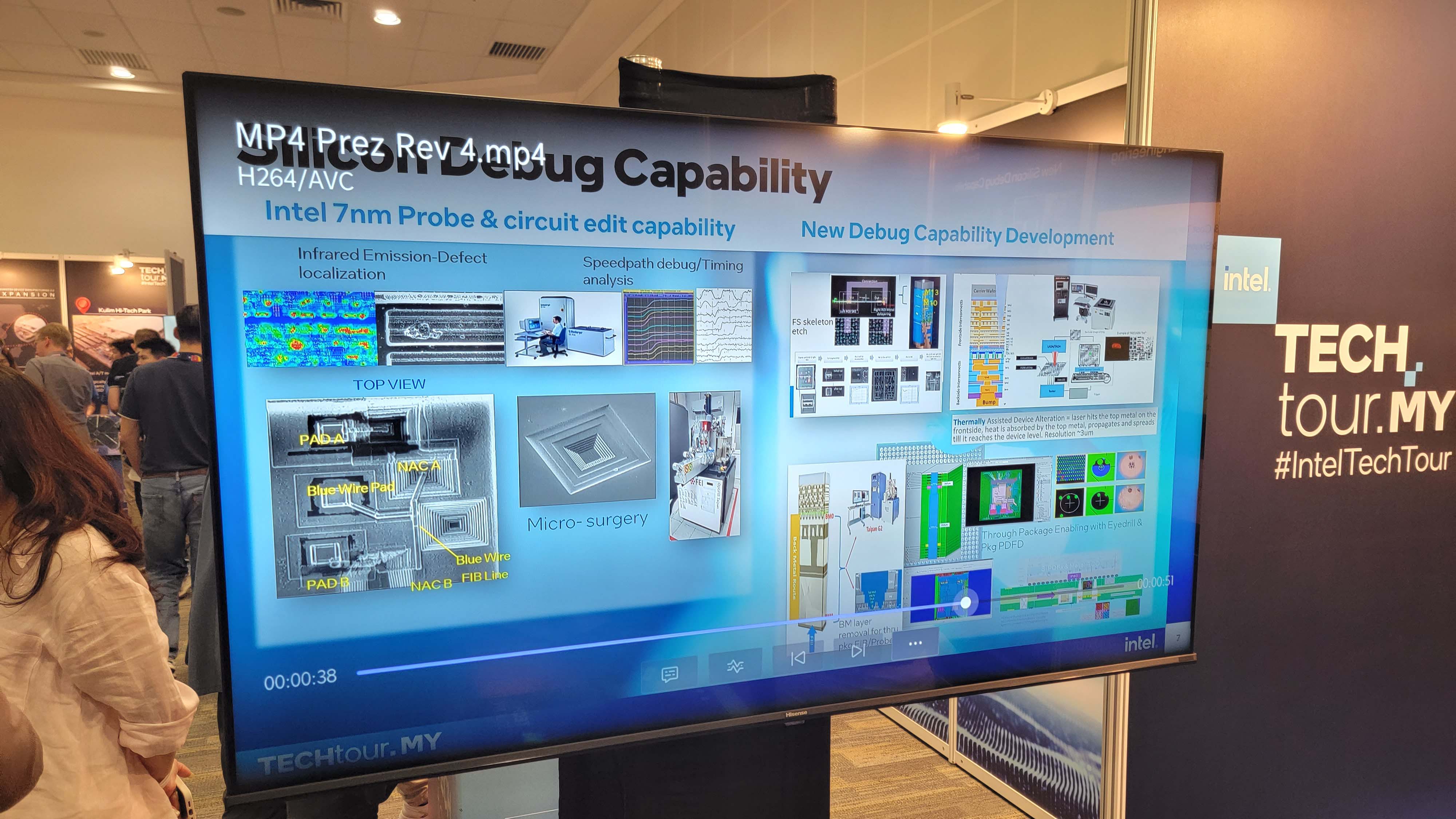
Intel's tour also included failure analysis labs, design and development (R&D) labs where it creates next-gen designs, and its department that creates the test tools that Intel uses in its facilities worldwide.
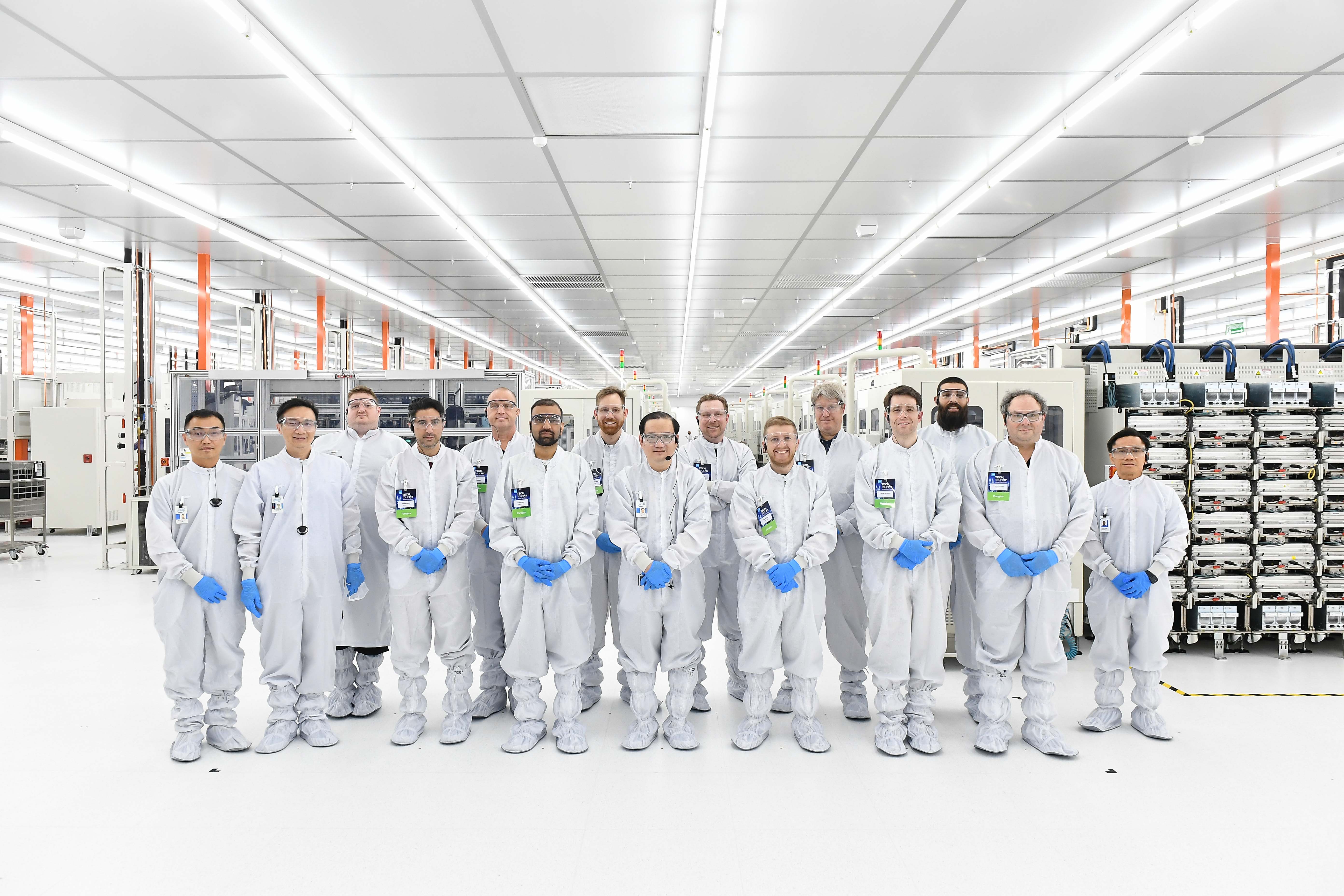
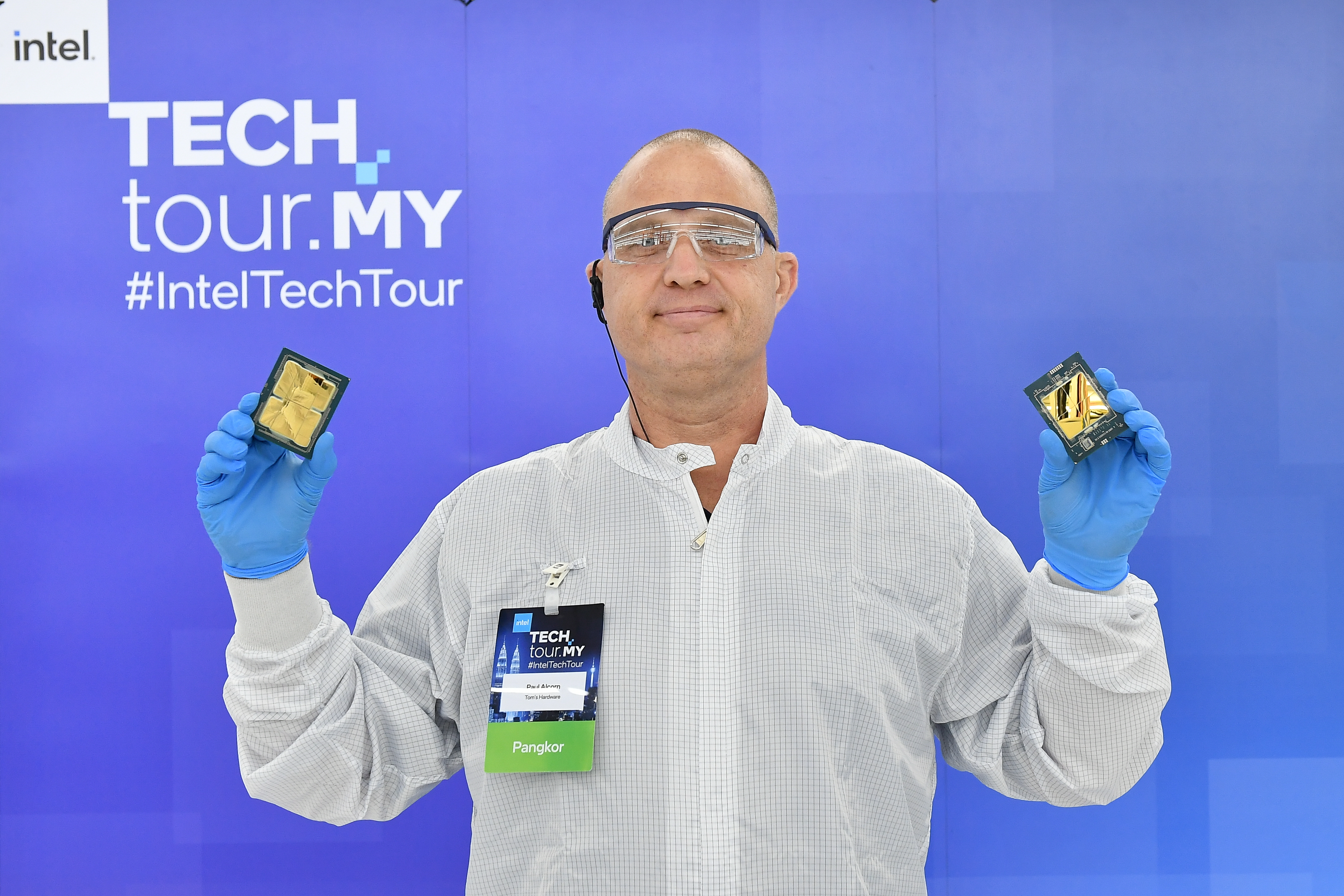
Each facility requires a certain level of 'bunny suit,' which is protective clothing to prevent damage to the machines and chips. A full bunny suit consists of a jumpsuit, feet coverings, latex gloves, hairnet, hood, mask, and protective eyewear. Other areas only required a lab coat, hairnet/beardnet, and safety glasses.
And with that, it's off into the factory we go.

Paul Alcorn is the Editor-in-Chief for Tom's Hardware US. He also writes news and reviews on CPUs, storage, and enterprise hardware.
-
Roland Of Gilead "If successful, those advanced nodes will grant Intel the lead over TSMC for the first time in years, " - so, the reasoning being here, that TSMC will be standing by scratching their arses during this same period. And thus Intel will overtake them!? Okay.Reply -
Paul Alcorn https://fuse.wikichip.org/news/7375/tsmc-n3-and-challenges-ahead/Reply
Intel will match TSMCs std cell density with the Intel 4 process by the end of this year. After that, roadmap projections indicate Intel will pull ahead. -
jkflipflop98 ReplyRoland Of Gilead said:"If successful, those advanced nodes will grant Intel the lead over TSMC for the first time in years, " - so, the reasoning being here, that TSMC will be standing by scratching their arses during this same period. And thus Intel will overtake them!? Okay.
No, you just inserted your own thoughts. No one is saying TSMC is going to stand still. We're saying they aren't going to be able to keep up. -
vertuallinsanity Intel utilized TMSC as a stand-in *partner* during a period of machinery teething issues.Reply
The intention of that partnership, for certain products, was always temporary in nature or Intel would have gone fab-less similar to AMD. Intel utilized TSMC to prevent bring-to-market delay while simultaneously reworking their fab processes and equipment to a viable state.
The article seems to imply TSMC makes their own processors or gpus and they're in direct competiton with Intel. They don't and they arent.
TSMC and/or Intel may trade process enhancement "blows" but Intel makes Intel CPUs for Intel and TSMC makes 'em for "anybody".
The article implication could apply to Apple, NVidia, AMD or others competing with Intel on similar node products.
Intel will continue to work with TSMC on GPUs and other product lines deemed fiscally feasible. Intel and TSMC are still partners.
There is no way anyone from Tom's hardware was allowed a tour of Intel's new ish.
Fact.. -
Roland Of Gilead Reply
No, you just inserted your own thoughts, in relation to my post!jkflipflop98 said:No, you just inserted your own thoughts. No one is saying TSMC is going to stand still. We're saying they aren't going to be able to keep up.
If you didn't notice, this article is one sided! I did certainly enjoy the tour and article in relation to Intel's tech, but there is zero context as to why TSMC 'might' fall behind.
You are right, no one is saying TSMC is gonna fall behind, but without context how is a reader supposed to know that? By checking the forums posts for an addendum article that gives the reasons why TSMC might fall behind? A bit of balance to illustrate these comments would help. -
td47 It would be interesting to know how Intel prevents IP and manufacturing methods/secrets from being exfiltrated from the Chengdu facility in China - given that country's penchant f or stealing and copying the Western Tech to try to catch up!Reply

