 Join Tom’s Hardware today


Penang Assembly and Test (PGAT)
The finished rolls of dies arrive at the Penang Assembly and Test (PGAT) facility for processing, a flow that includes multiple steps:
- Chip Attach: The die is taken from the reel and attached to a PCB substrate.
- Epoxy: Epoxy is placed between the die and the PCB to ensure even distribution of stress.
- Lid Attach: Thermal Interface Material (TIM) is placed atop the die, and then an Integrated Heat Spreader (IHS) is attached to the package over the die.
- Burn-in: Finished CPUs are sent for stress testing at high temperatures and voltages to detect defects.
- Test: Another series of electrical tests are performed to ensure functionality.
- Platform Performance Verification (PPV): The chip is tested in an environment that mimics end-user platforms and conditions.


Above, we can see the complex multi-die chip packages the PGAT facility creates by mounting the dies onto a PCB/substrate. The first image shows Ponte Vecchio chips both before (right) and after the epoxy application process, which comes after the chips are bonded to the PCB. As you can see, the epoxy lines the edges of the dies on the package.
The Chip Attach process begins by mounting the different reels with different types of chiplets into another pick-and-place machine that strips the needed dies and places them on the PCB. Intel demonstrated this process by mounting four dies on a PCB to create a Sapphire Rapids package. The dies are placed atop a PCB, and a thermo-compression machine heats the chip to bond the tens of thousands of solder bumps on the PCB to the solder bumps on the bottom of the die. This process heats the die to 300C for an unspecified amount of time, thus forming the critical connections that allow the chip to communicate with its host.
The Chip Attach process requires absolute precision to mate the solder bumps precisely, so the system uses advanced optical alignment to align the die perfectly on the PCB. The somewhat flexible die is also held perfectly flat with a vacuum system that applies suction to the full span of the die. Meanwhile, a similarly suction-powered plate holds the PCB in place.
After being fused to the PCB, a tiny air gap remains between the die and the PCB. This can lead to uneven stress when the integrated heat spreader (IHS) is applied next or when an end-user torques down a CPU cooler. That's not to mention that the daily thermal expansion and contraction that occurs during the chips' lifespan could lead to cracked solder bumps.
To rectify that issue, Intel applies a layer of epoxy resin between the PCB and the die, but it doesn't inject the fluid directly into the air gap. Instead, a nozzle (or two, in some cases) applies epoxy along the edge of the die, and the capillary effect does the rest, allowing the epoxy to spread evenly underneath the die.
Intel applies this epoxy to either one, two, or three sides of the dies, depending upon the size and complexity of the chip. You can see the capillary effect in action 18 seconds into the above video. Intel then employs a non-destructive ultrasound scan of the chip to check for air gaps in the epoxy underneath the die, though we were told that finding them is a rare occurrence.


Some of the chips now move on to the Lid Attach process (mobile chips don't have an IHS). Intel first applies a Thermal Interface Material (TIM), such as standard pTIM (polymer TIM) for most mainstream processors, or sTIM (Indium Solder TIM) for chips that require more substantial cooling.


After applying the TIM to the die, an adhesive is placed around the die area where the edges of the integrated heatspreader (IHS) will mate with the PCB. The machine then places a heatspreader on top of the package and compresses it while applying heat.
We learned that solder TIM requires much longer heating and compression time and significantly higher temperatures than standard pTIM. It also requires that the die be first prepared with a special coating before solder is applied, thus adding more time to the process flow. We weren't given any indication of how much longer the cycle rate is, though we were told it significantly reduces throughput.
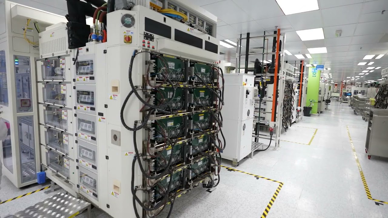
The processor then goes through a Burn-In testing process that employs high temperatures and voltages over an extended period to check for defects. Like Intel's other test machinery, the custom High-Density Burn-in (HDBI) tester machine tests multiple chips in parallel to increase testing throughput. Intel didn't provide any pictures of the full machine (parts of it are visible in the SIMS section on the following page), but it is massive. The machine can simultaneously test multiple types of chips, from Ponte Vecchio to Meteor Lake. It is here that the chips are binned into different variants depending on their characteristics and the number of functional units (CPU and GPU cores), thus assigning the chips as Core i9, i7, i5, or i3, for instance, or as an F-series model that has a defective graphics unit.
The testing doesn't stop there. After Burn-In, the chip moves to a series of electrical tests and then moves on to the Platform Performance Verification (PPV) stage that mimics real-world use. The PPV testing phase employs a System Level Tester machine to bombard the chips with various real-world workloads while the chip runs an operating system, like Windows, then cycles through other tests as it runs another operating system, like Linux.
Intel didn't divulge how many types of operating systems it uses for this stage. Intel didn't share pictures of the System Level Tester, its own internally-designed custom machine, but some can be seen starting at 2:30 in the video below and in the SIMS section on the following page. These machines also test with emulated external I/O devices attached, like storage and USB devices and the like, to check all of the chips' functions.
Some chips don't pass these rigorous tests, so they head out for further inspection at the failure analysis lab.
