Join Tom’s Hardware today


Failure Analysis Lab
Every die wants to live, but some don't. Those defective chips end up in the failure analysis lab for a series of tests to determine the nature of the fault and then, if needed, a series of deeper tests that can be destructive.
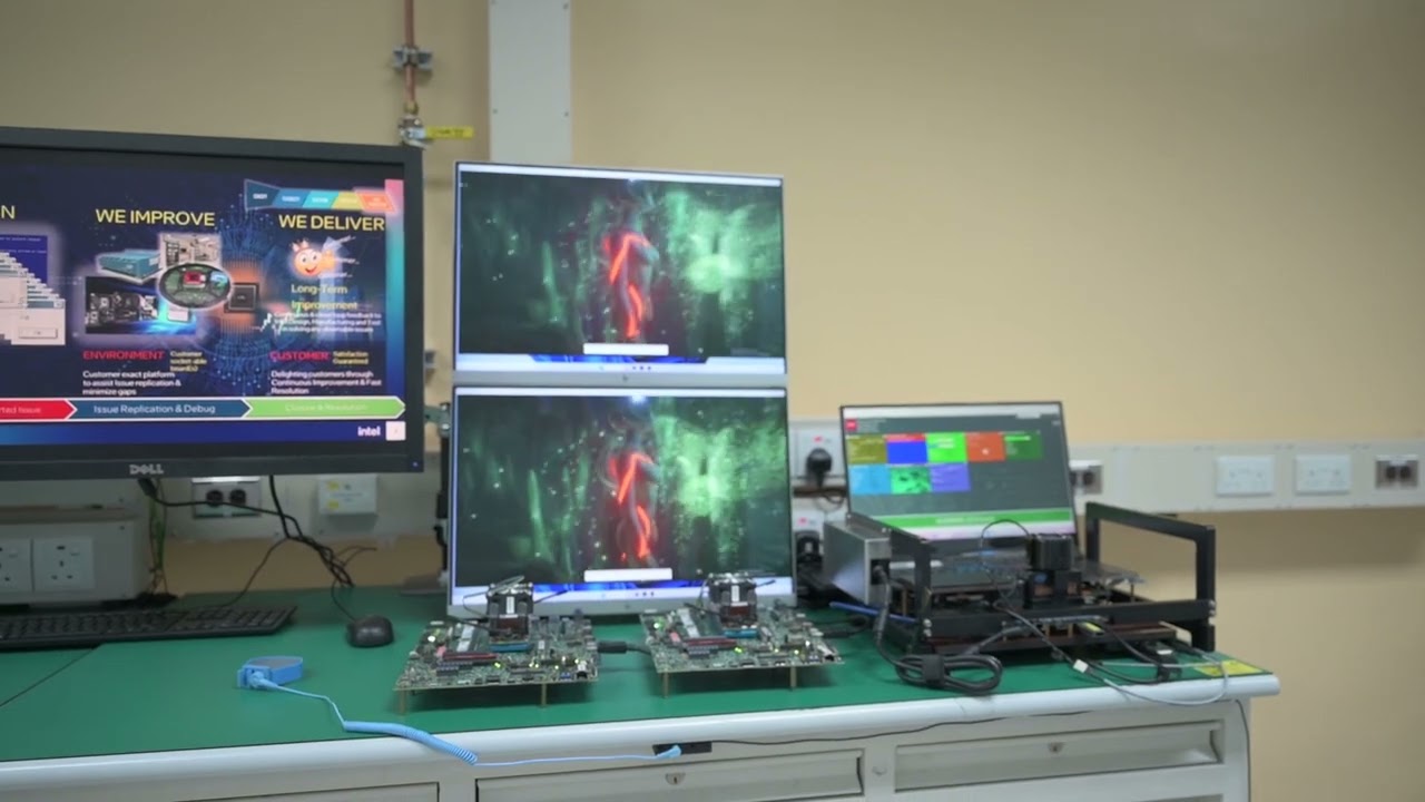
The above video shows a neat representation of one type of failure that can be seen during a 3DMark test. This demonstration shows two chips running the same sequence, with the defective chip running the program on the top monitor and the fully functioning chip running on the monitor below. During the first few seconds of the video, you can see a series of artifacts that manifest as bright lights at the bottom right of the monitor on the defective chip, and that's indicative of an error in the chip.


This chip had passed many layers of testing throughout the manufacturing process, but the defect was found during the PPV stage. As you can imagine, finding random errors such as this in chips that fully pass stress and electrical error testing can be a daunting task, but finding the source of the issue can be an even more challenging endeavor.


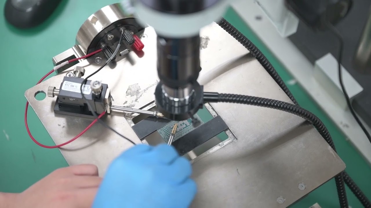
Intel employs a range of testing techniques, including ultrasound, infrared, and sonar, to isolate defects and study the failed processors. After locating the defect, destructive methods, like grinding or using an ion beam, can be used to study the issue further. This information is fed back to the design teams to help develop newer steppings of processors or refine production production processes to stamp out recurrent bugs, if necessary.
Malaysia Design and Development Lab (MDDL)
The Malaysia Design and Development Lab (MDDL) is responsible for large-scale testing to help validate new processor designs and IP. The teams in this area work on pre-release silicon and help validate core IP, like E-core and P-core silicon, SoC designs, and chipsets, by passing the chips through a barrage of real-world testing.
This team focuses on large-scale parallel testing to find any bugs in the new chips that come from Intel's research and development teams, ultimately helping to pave the way to mass production. This often includes fully stressing the device with every single form of I/O attached, like multiple monitors, GPUs, keyboards, mice, USB devices, Thunderbolt connections, storage devices, and other peripherals, all while conducting a series of stress tests under real-world operating conditions.


Unsurprisingly, this was one of the most closely guarded areas we saw on the tour. We were given a demo about Intel's future E-cores in a section that oddly had aisles upon aisles of empty shelves. We were told the systems in the area had all been removed prior to our arrival because they were testing unreleased products. Notably, this area was used for our 'Next-Gen E-Core' demo, so it's safe to assume the chips under test were of the Sierra Forest variety.


These teams are also responsible for power and thermal characterizations for new processors, helping to ultimately dial in the correct mixtures of voltage and frequency to assure stable operation. Other teams collaborate with Intel's customers to help them develop highly-tuned system designs to accommodate the newest chips, often by directly doing the tuning themself, other times by providing reference boards and designs.
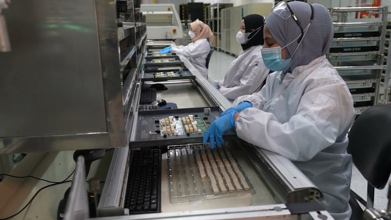
System Integration and Manufacturing Services (SIMS)
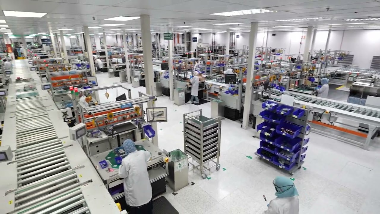
Unbeknownst to many, Intel has its own assembly line that creates high-tech testing devices for its facilities worldwide, and it's based in Kulim.
The System Integration and Manufacturing Services (SIMS) factory produces test equipment like Intel's High-Density Burn-in (HDBI) tester that's used for Burn-In stress testing for Intel's processors, as we outlined in the Assembly and Test section. You can see parts of that machine in the first six images in the album below.


This group also the High Density Modular Tester that Intel uses to test and classify its chips before they're sent to be affixed to PCBs, and the System Level Tester machine that's used for testing under real-world conditions with actual operating systems and peripherals attached to the host system. That's pictured in the last image in the above album.
This group also creates Intel's Reference Validation Platforms (RVP), which are custom motherboards used during the development phase of any new chip. In fact, they manufactured the platforms we saw at Intel's Overclocking Lab a few years ago, not to mention a host of other equipment that Intel uses for testing its products at its global facilities.
These products are largely made with physical labor, there isn't a lot of automation in this area, but Intel manufactures these products itself to protect the development of its proprietary internal technologies.