Inside Intel's Secret Overclocking Lab: The Tools and Team Pushing CPUs to New Limits
We get an exclusive tour of the facility where Intel pushes chips to their absolute limit.
Mainstream Reference Validation Platforms
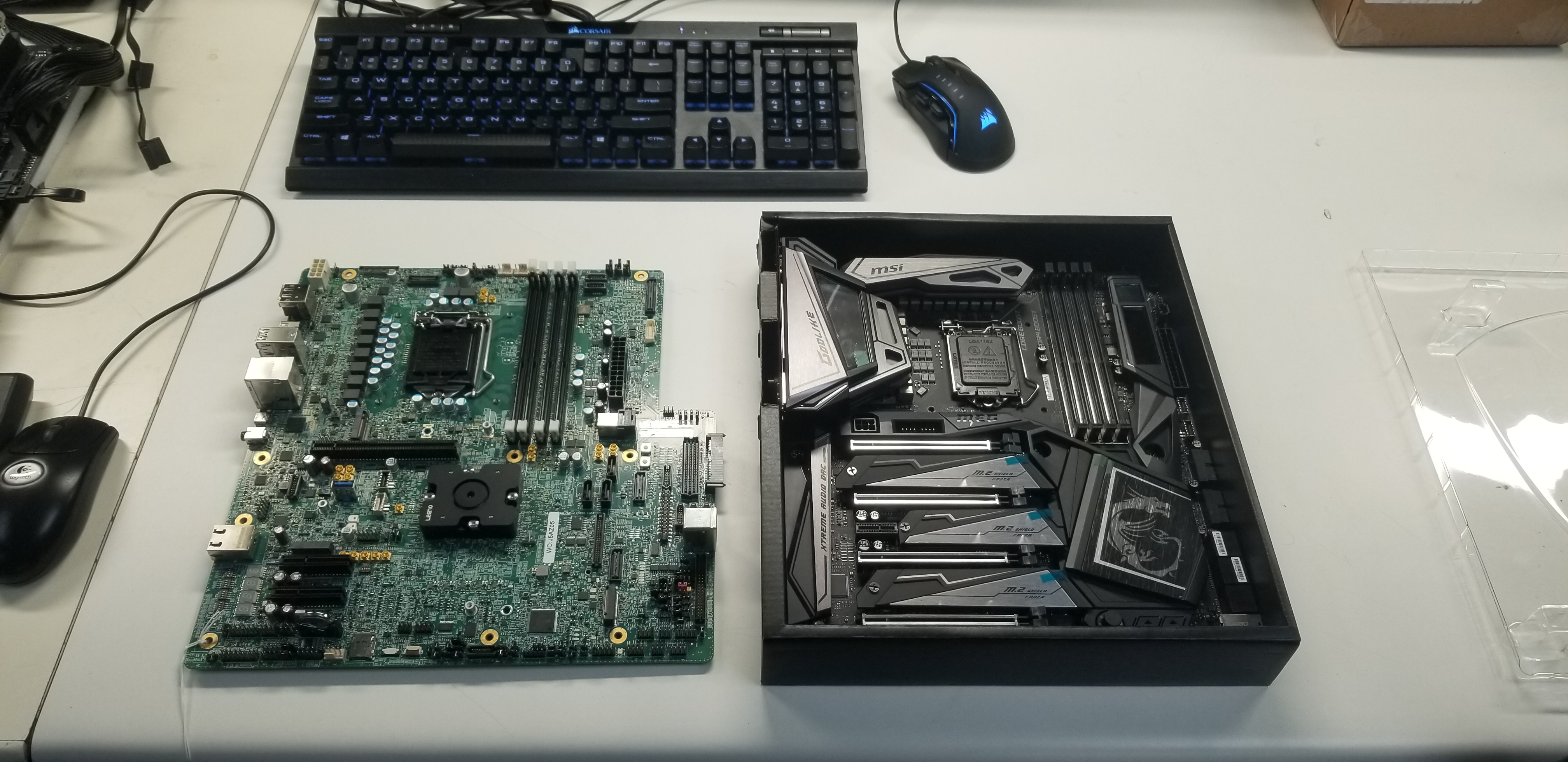
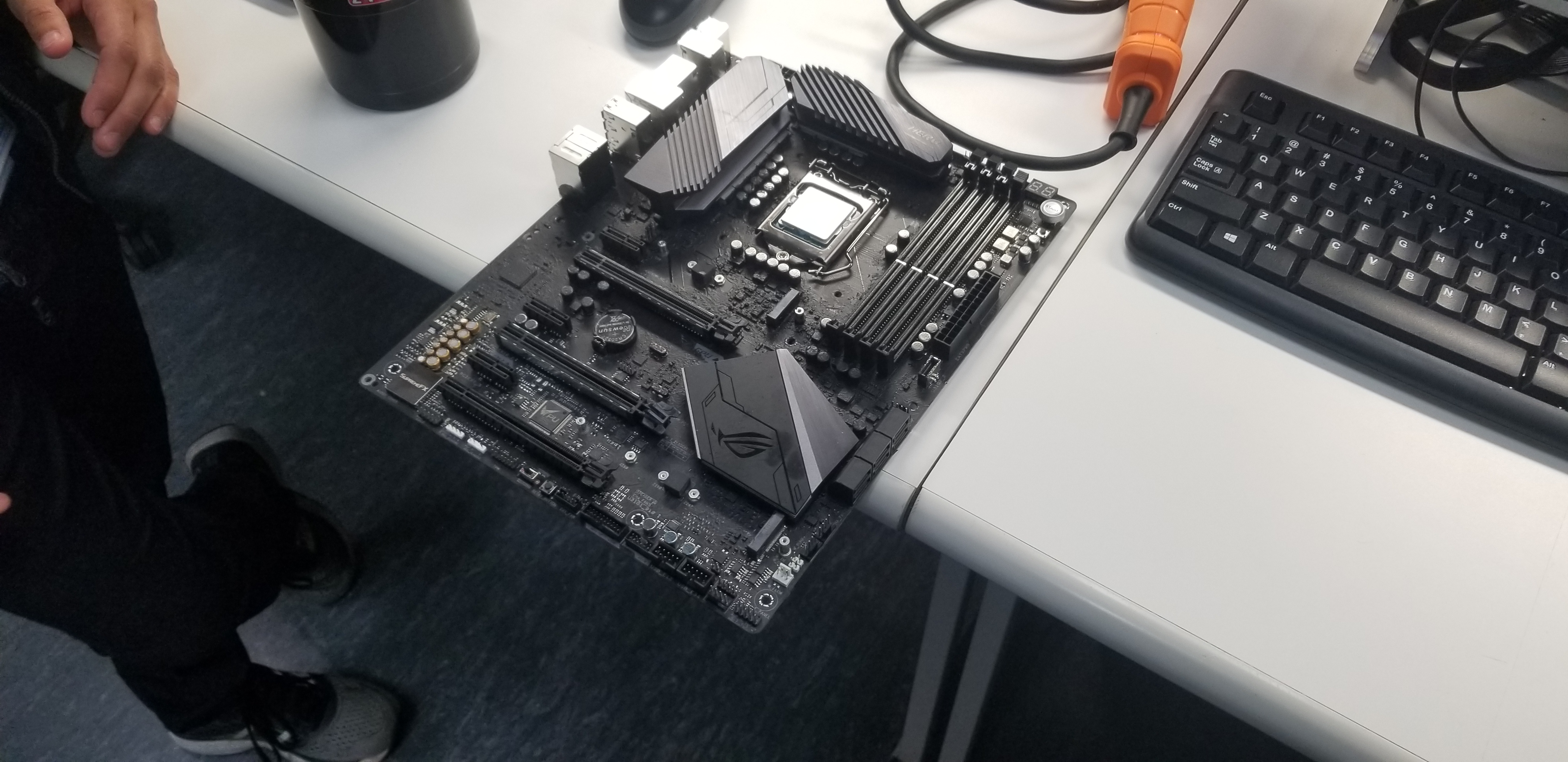
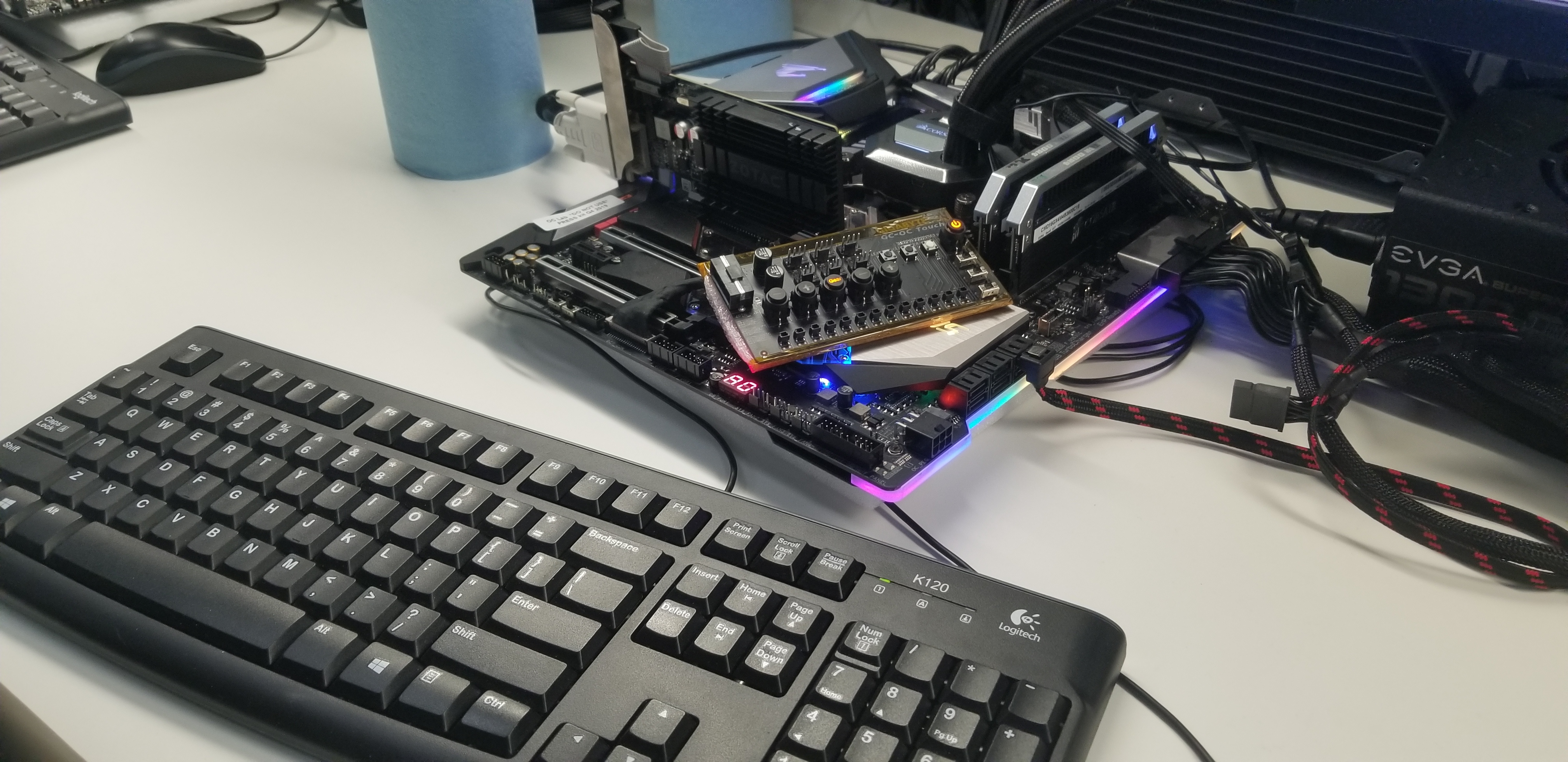
The overclocking labs' primary remit is to ensure that Intel's processors are designed and optimized for overclocking, but that same initiative extends to the platforms (i.e., motherboards) that play a huge role in determining how well you can overclock your chip.
That means the team has to work with vendors to make sure their motherboards are fully optimized for overclocking, and we found boards from every major vendor, like MSI, ASRock, Gigabyte, EVGA, and ASUS, in various stages of overclocking testing, and with various types of cooling solutions, scattered throughout the lab. Intel tests these boards and gives feedback and advice to vendors.
But the team is also responsible for making sure that Intel's own internal teams have platforms that are representative of the end products enthusiasts and overclockers will purchase. As we can see in the first image in the album above, Intel's previous-gen reference validation platform (RVP - left) for mainstream processors is a rather simple affair that lacks the generous accommodations we can see on MSI's Godlike motherboard on the right.
Sure, there are accommodations for some of Intel's internal testing tools and swappable PCH's that we'll cover on the following page, but features like the power delivery subsystem, not to mention finer aspects like optimized memory trace routing that facilitates higher overclocks, are far behind even most garden-variety Z390 motherboards on the market.
That's one of the first disconnects the team worked to solve, and it's an ongoing effort.
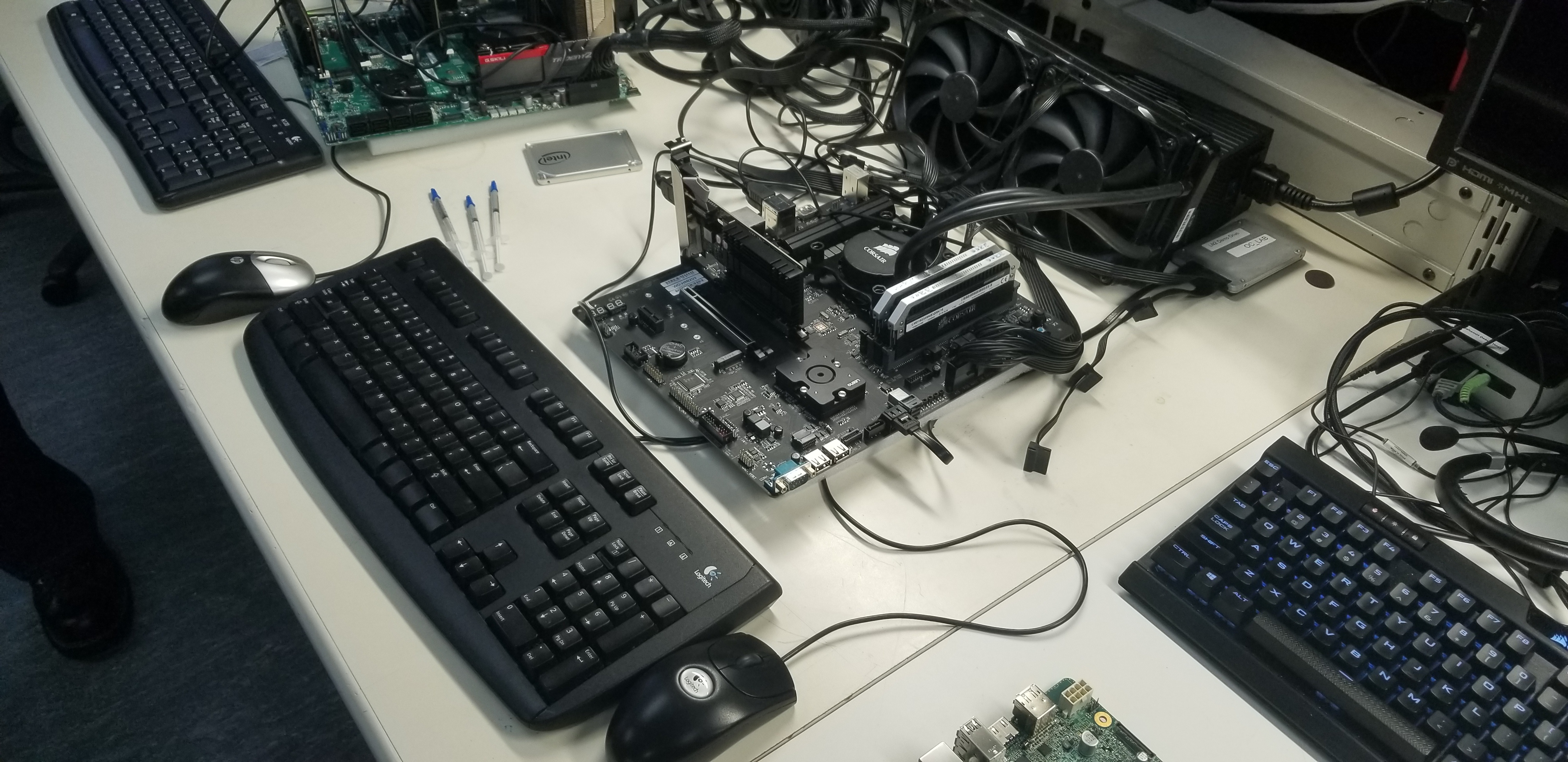
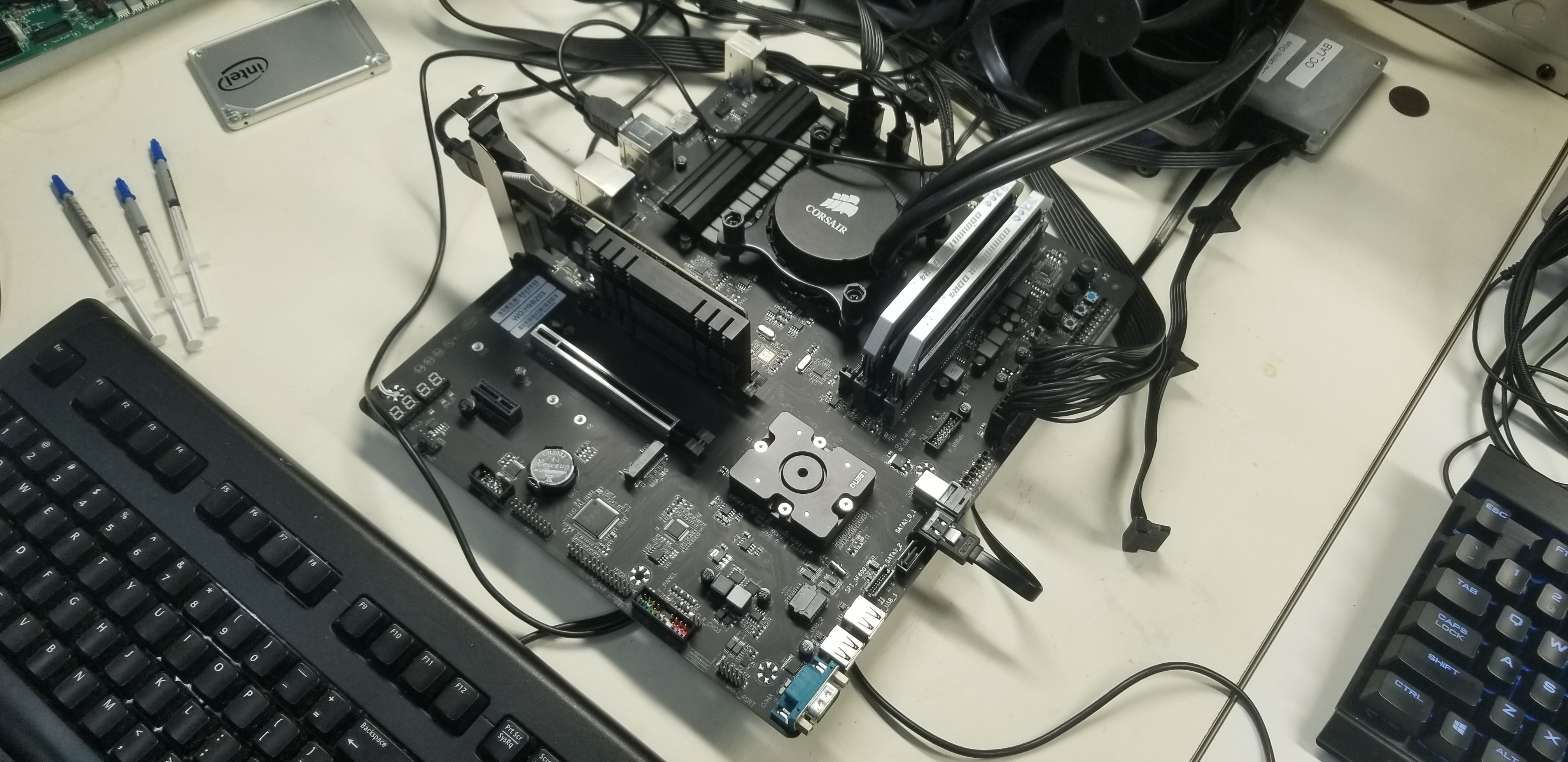
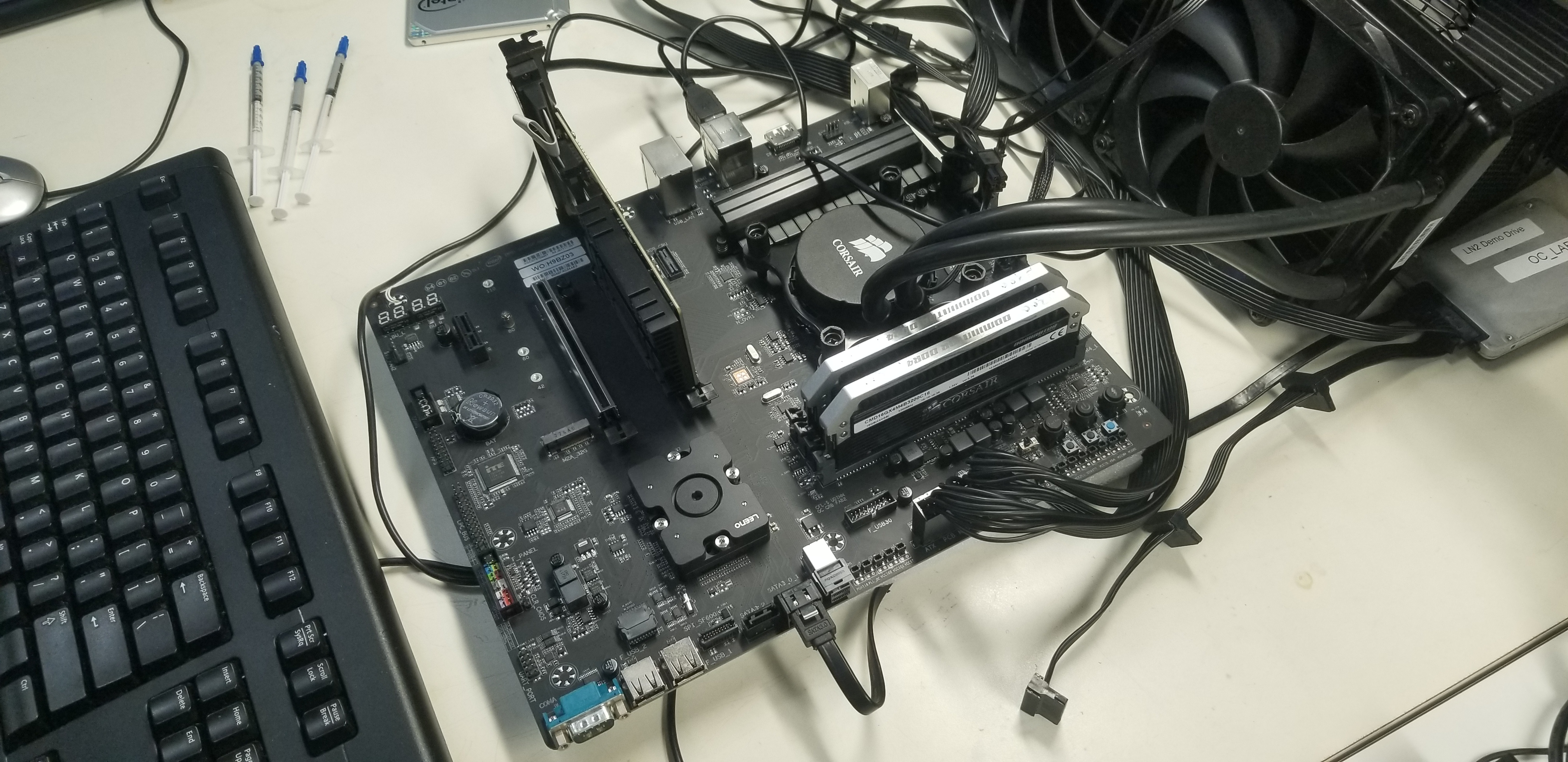
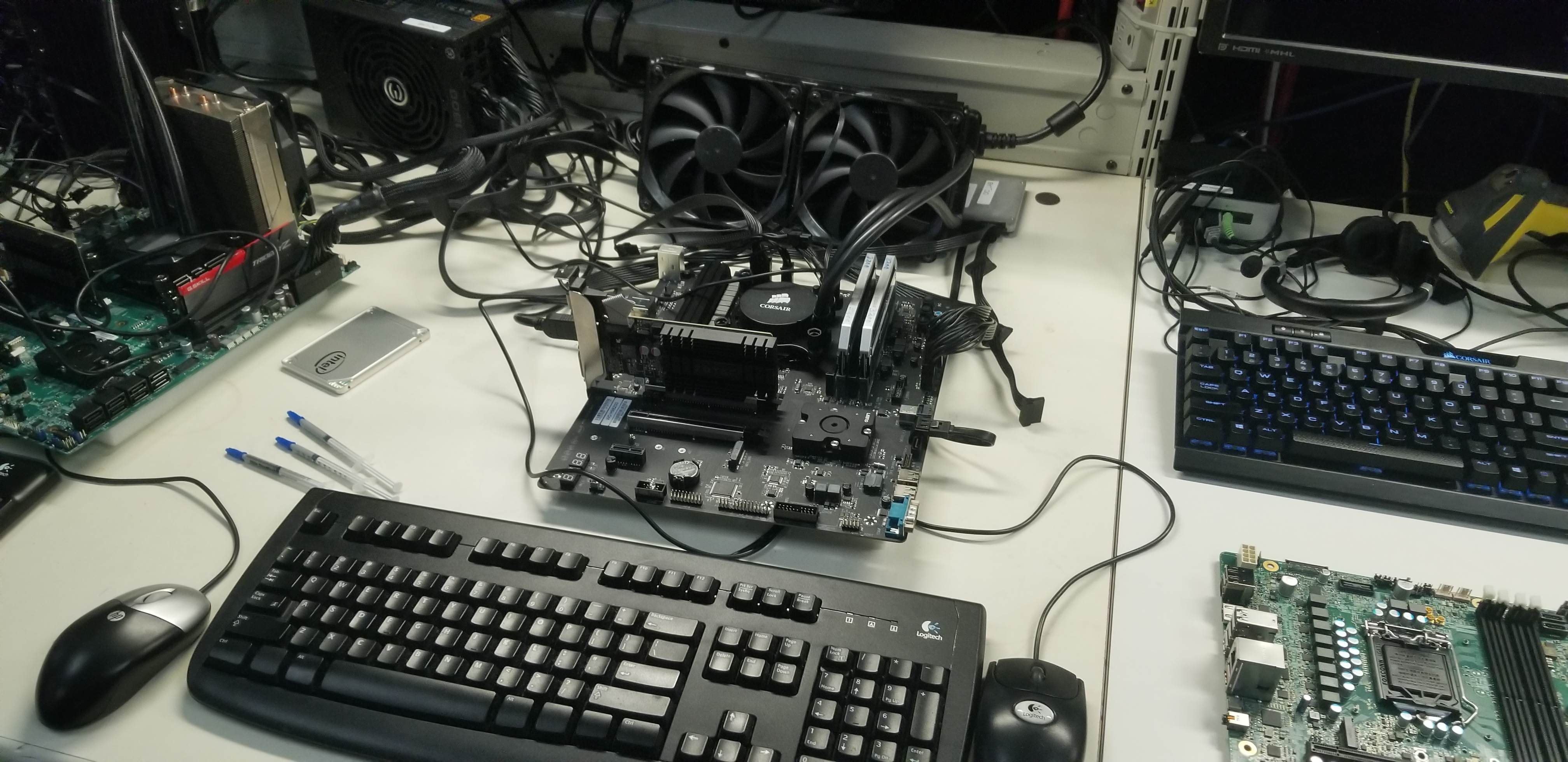
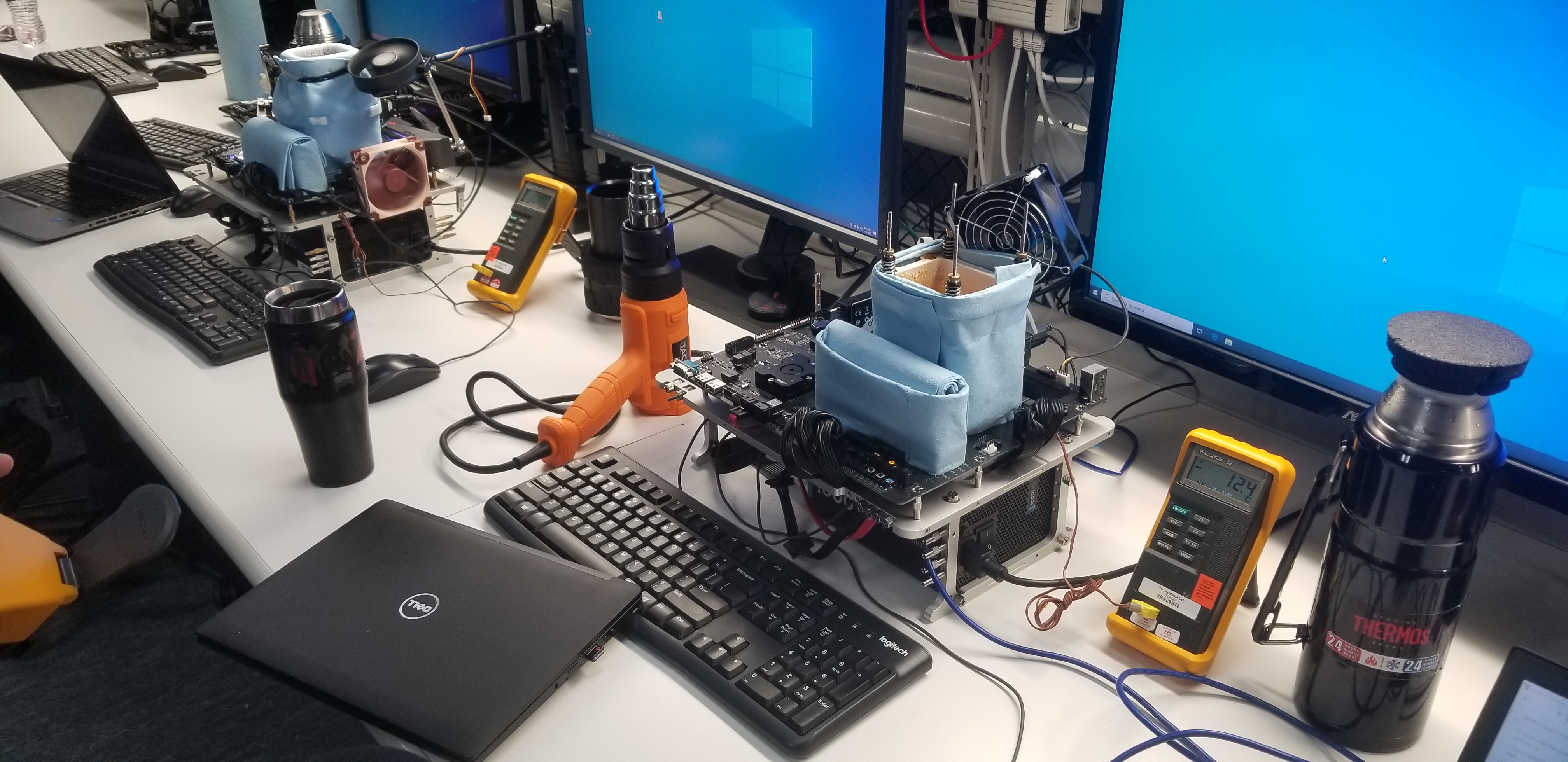
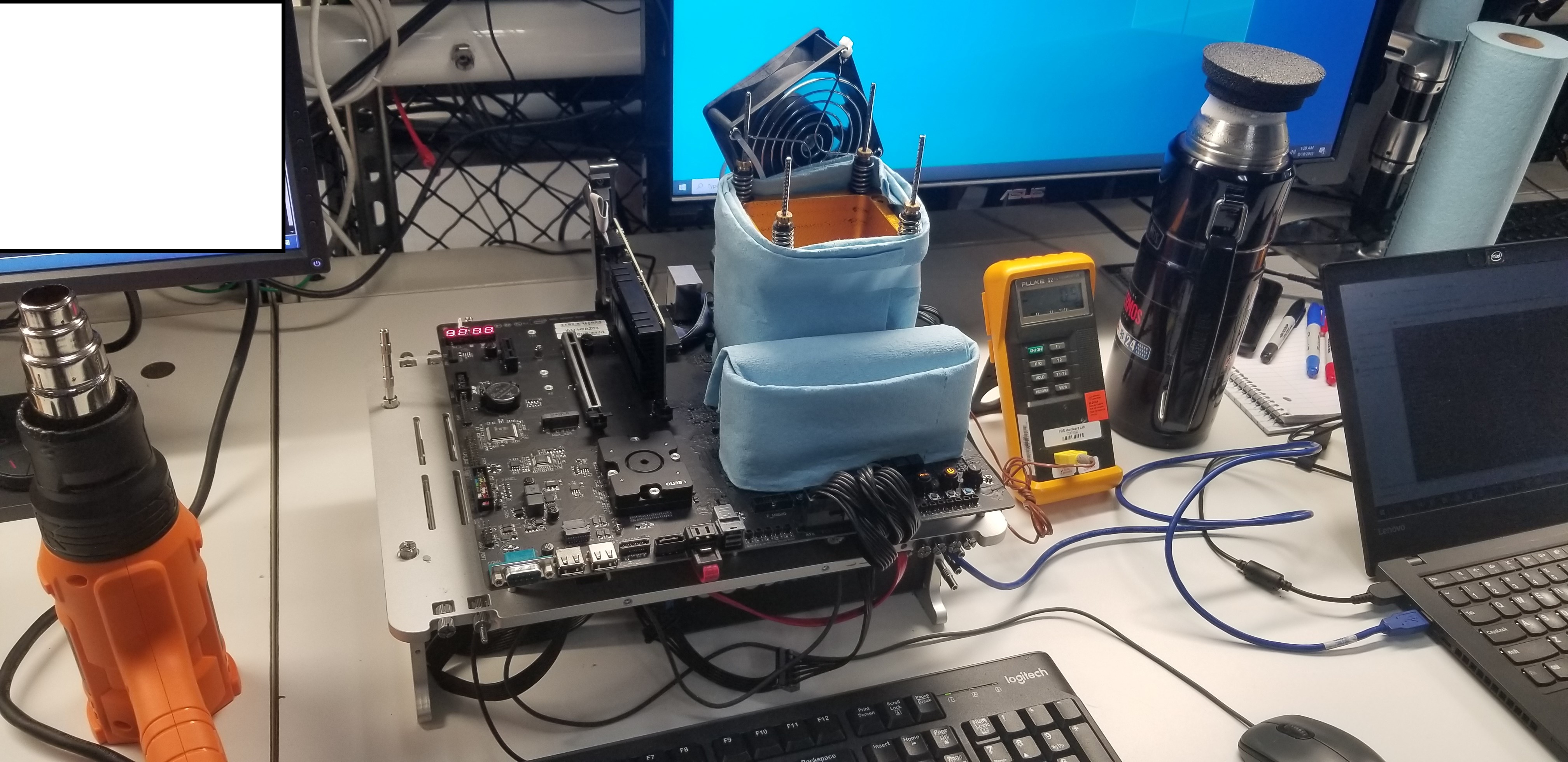
The lab team worked with Intel's reference validation platform (RVP) team to design newer platforms that look, and act, a lot more like what you would expect from an enthusiast-class motherboard. The boards are still quite spartan and lack the RGB goodness, OLED screens, and other fanciful trimmings of today's flagship boards, but Intel beefed up the power delivery subsystem for the chip and memory, along with adding meaningful VRM cooling. You can see they also stepped up from a single eight-pin EPS by adding an additional 4-pin connection for CPU power.
The team also made other adjustments, like fine-tuning the memory traces to improve memory overclockability. We also see they added some useful power and reset buttons for the lab crew, and metal reinforcements for the PCIe slots. We're sure the new digital debug display also comes in handy.
Get Tom's Hardware's best news and in-depth reviews, straight to your inbox.
Those are just our external observations, though: the team tells us that it asked for roughly 100 new features to bulk up the existing validation platform. Many of these features will probably never be explained to us fully, but we're told there are plenty of new hooks and features for measuring performance and debugging issues. We'll cover some of those features on the following page.
As mentioned, this is still a board whose primary mission is validation, so it isn't the fanciest-looking affair. In either case, the team demonstrated some solid overclocking action with the new board under LN2, so it's clear that it's succeeding in its mission to bring overclocking closer to the chip design and validation process.
The OC lab team has broken many world records in its lab with the OC RVP boards, and the first world record that fell with the new RVP board was a big moment for them: That told them the design was ready.
But you won't ever see those records posted to HWBot: Intel has a policy of not competing with its customers, so Intel employees can't submit benchmark runs. The team has access to god-like tricks that aren't available to us regular users, so that's a good policy.
That doesn't preclude internal competitions, though, and there is a running competition among Intel employees for overclocking records. The competition extends to enthusiasts in other Intel labs, too. (For the record, Navya Pramod is currently 'spanking everyone').
As a side note, you'll notice Intel uses pretty basic video adapters for testing, and I didn't notice any flagship AMD or Nvidia GPUs scattered about the lab. That's primarily because these slim adaptors are more suitable for overclocking testing as it allows easier access to bolt on various cooling solutions.
High End Desktop (HEDT) Reference Validation Platform
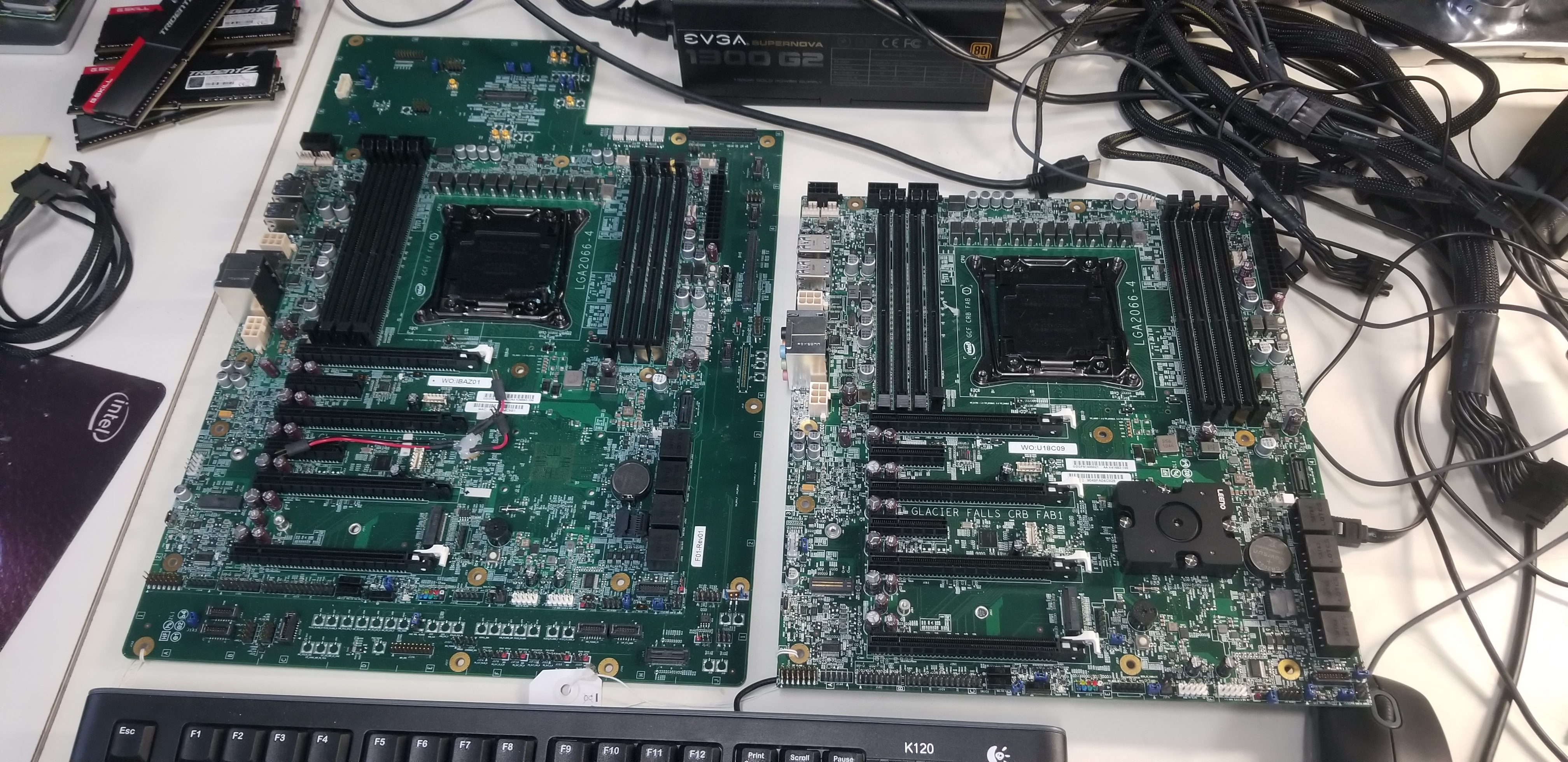
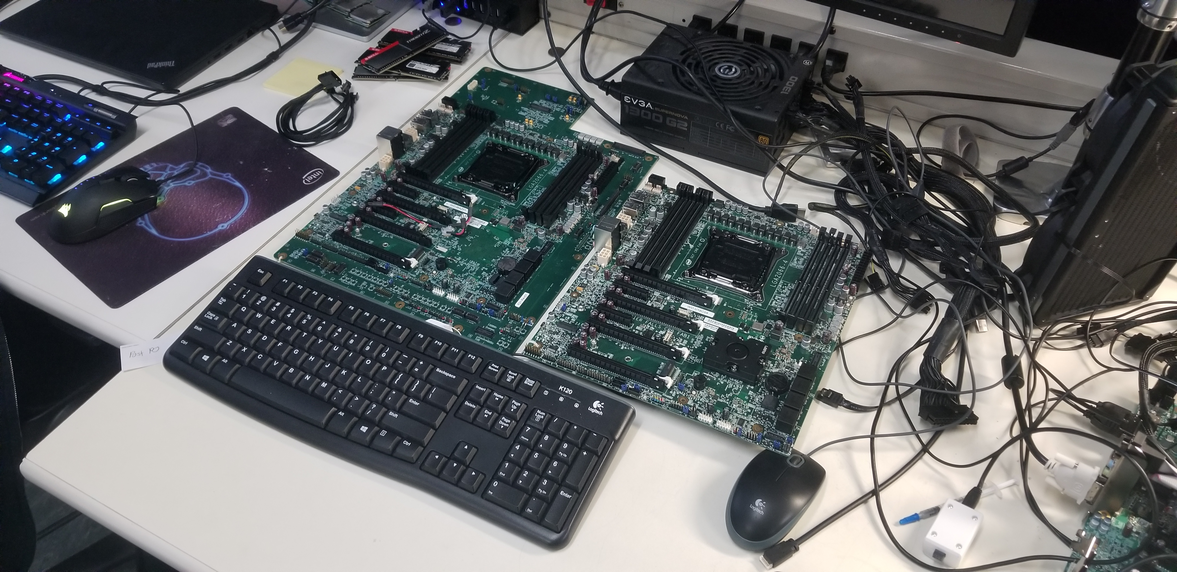
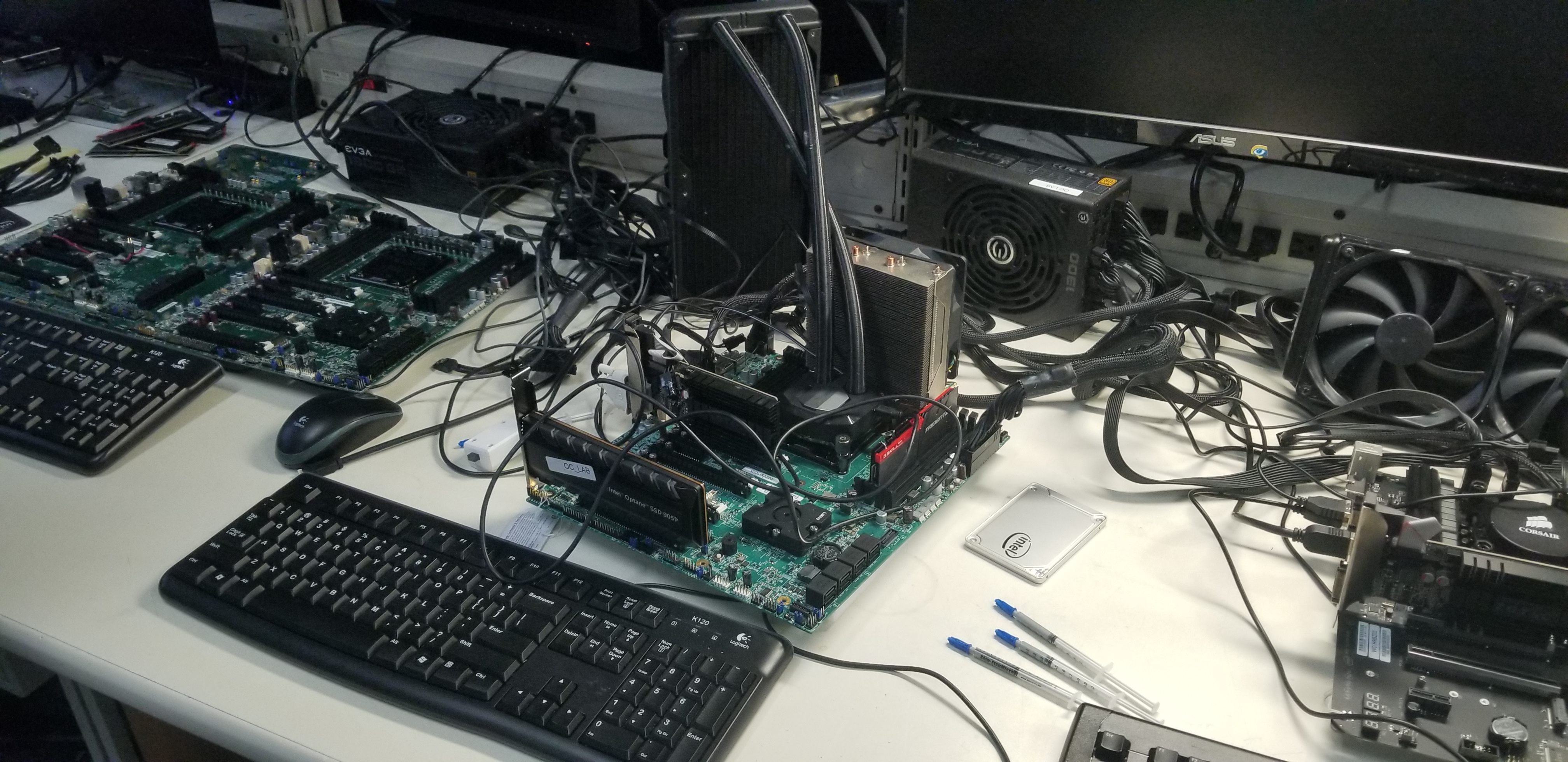
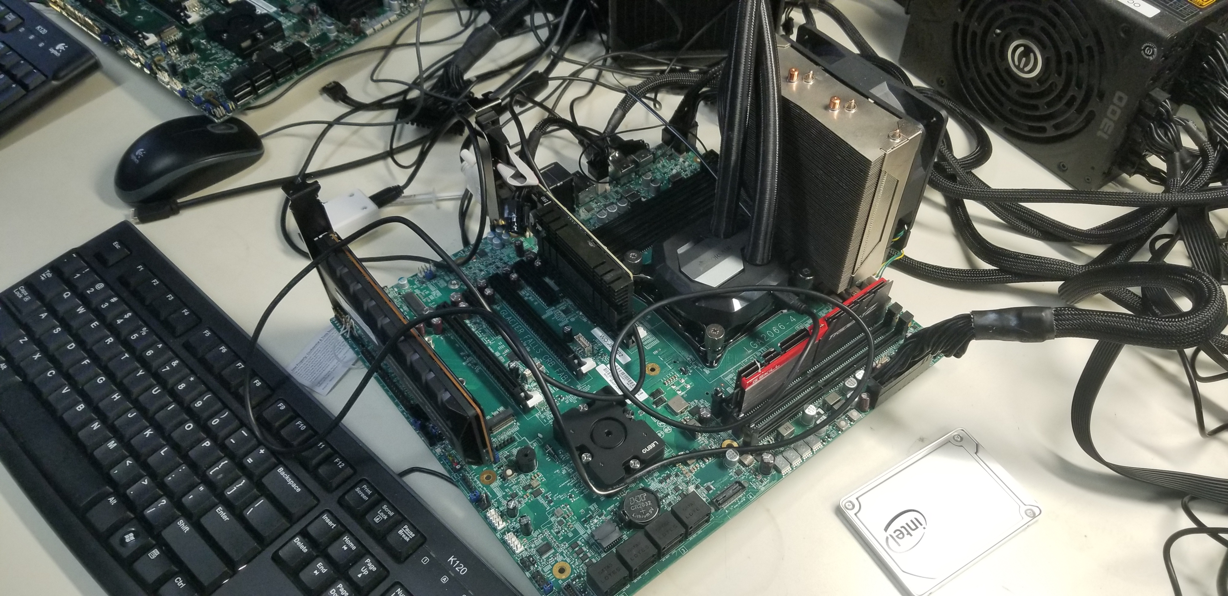
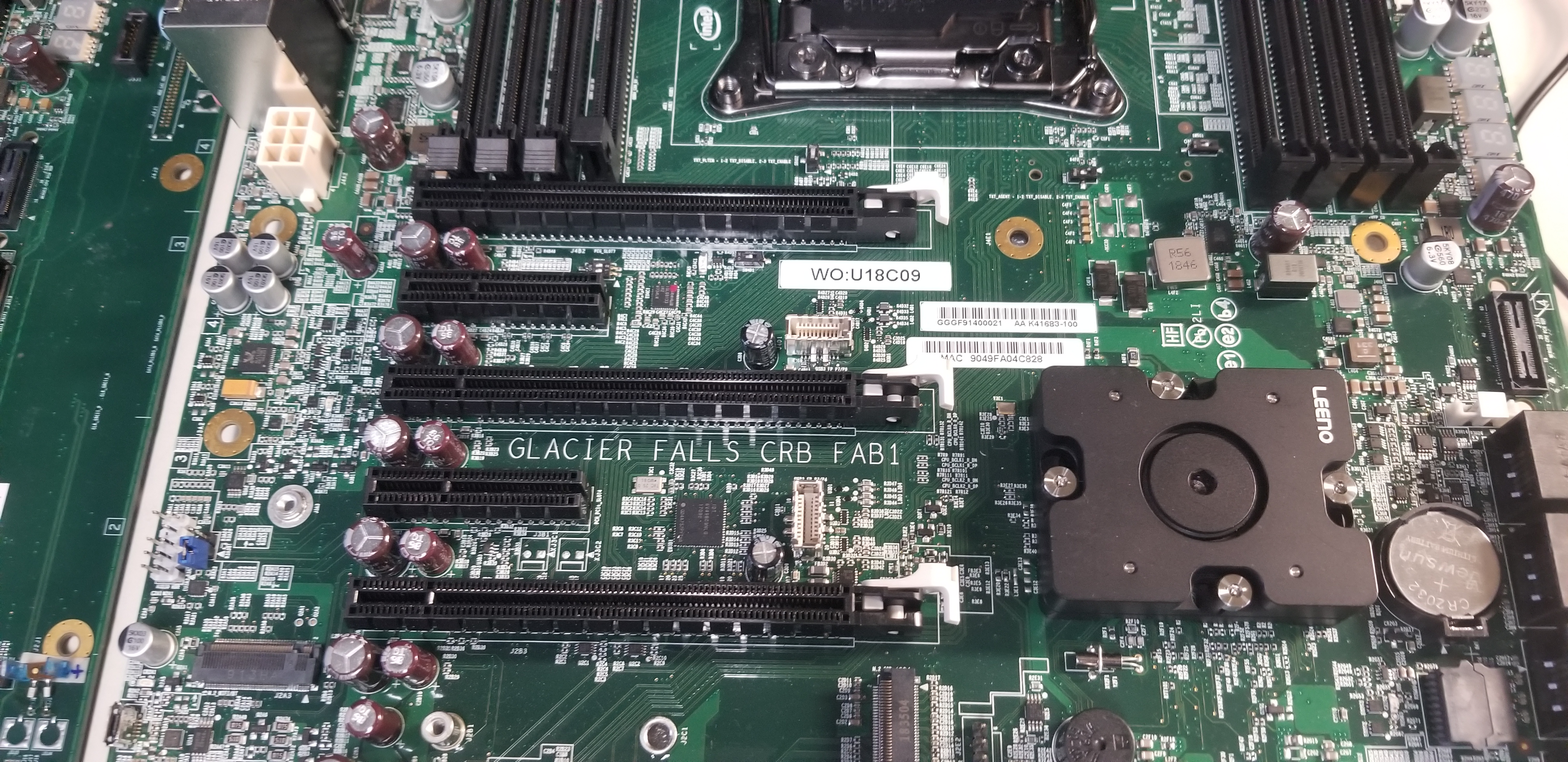
Here we see a few permutations of Intel's internal HEDT RVPs. The HEDT chips are designed for high-end enthusiasts, so we're told they've had plenty of overclocking-capable features from the onset. The team continues to drive more features into the platform and is also working on a beefier OC RVP solution to sidestep some of the challenges associated with HEDT overclocking. As you can see, there's a massive VRM cooler attached to the board next to the CPU cooler, which we'll cover on the following page.
Overclocking Bootcamps
The team continuously works closely with motherboard vendors to optimize their boards, but that work intensifies as they prepare new generations of CPUs for launch. Intel holds two-day overclocking bootcamps for motherboard vendors to help speed the process.
Teams from motherboard vendors descend from around the globe on the overclocking lab for the event. Intel also flies in its own experts from around the world, like its power management team (p-code engineers) from Israel, debug teams, memory reference teams, and BIOS teams.
The goal is help the motherboard vendors understand the new chips and optimize their platforms for overclocking, so the motherboard vendors send their top engineers, like legendary board designers and overclockers Nick Shih (ASRock), Shamino (Peter Tan, ASUS), Toppc (MSI), and HiCookie (Gigabyte), along with teams of their BIOS and hardware engineers. Many of the motherboard vendors also have teams on standby in Taiwan that they communicate with throughout the event to address issues quickly, often working around the clock to maximize their time at the event.
The event originally ran from 8am to 11pm until Intel instituted a 'mercy' rule that constrained the official working hours from 8am to 8pm. That doesn't stop the motherboard vendors from taking gear back to their hotel rooms, though.
These overclockathons result in higher-quality overclocking gear for enthusiasts, but those same features and learnings bleed over to mainstream products, too, highlighting that the work the overclocking lab does impacts all facets of Intel's consumer desktop business.
Make no mistake, overclocking is a big business for motherboard vendors, too. They also regularly work with leading overclockers, like L0UD_SIL3NC3, mllrkllr88, and Splave, among many others, to optimize their platforms and make world records on their platforms. Everyone wants to be on top, and as a result, some motherboard vendors also bring their sponsored overclockers to the event, too. Intel often gives the professional overclockers trays of processors to bench during the event, which we're told becomes a sideshow all its own.
- PAGE 1: The Overclocking Lab
- PAGE 2: The Beginnings and Mission of Intel's Overclocking Lab
- PAGE 3: Pouring LN2, the OSHA Way
- PAGE 4: TIM, Coolers, The Medusa, and Other Intel Lab Gear
- PAGE 5: Validation Boards and Overclocking Bootcamps
- PAGE 6: VRM Supercooling, PCH Swapping, and Internal Tools
- PAGE 7: 'Safe' Overclocking Voltages and Techniques
- PAGE 8: Is Overclocking Dead?
MORE: Best CPUs
MORE: Intel & AMD Processor Hierarchy
MORE: All CPUs Content
Current page: Validation Boards and Overclocking Bootcamps
Prev Page TIM, Coolers, The Medusa, and Other Intel Lab Gear Next Page VRM Supercooling, PCH Swapping, and Internal Tools
Paul Alcorn is the Editor-in-Chief for Tom's Hardware US. He also writes news and reviews on CPUs, storage, and enterprise hardware.
-
Paul Alcorn ReplyDark Lord of Tech said:Can you get the AMD tour? Would love to see that.
I'll jump on a plane the second it is offered :) -
bit_user @PaulAlcorn , thanks for the awesome piece!Reply
I'm still making my way through it, but wanted to draw special attention to this bit:
the engineers told us they feel perfectly fine running thier Coffee Lake chips at home at 1.4V with conventional cooling, which is higher than the 1.35V we typically recommend as the 'safe' ceiling in our reviews. For Skylake-X, the team says they run their personal machines anywhere from 1.4V to 1.425V if they can keep it cool enough, with the latter portion of the statement being strongly emphasized.
Thanks for that!
At home, the lab engineers consider a load temperature above 80C to be a red alert, meaning that's the no-fly zone, but temps that remain steady in the mid-70’s are considered safe. The team also strongly recommends using adaptive voltage targets for overclocking and leaving C-States enabled. Not to mention using AVX offsets to keep temperatures in check during AVX-heavy workloads. -
StewartHH Some one should comparison between different vendors die size like Intel 10nm vs AMD 7nm to see if there is actually performance gain. I would use per-core speed and not taking multiple cores into account.Reply -
bit_user @PaulAlcorn , uh oh. Now that I just finished heaping praise, I've got a gripe. In the penultimate paragraph:Reply
... assures that the learnings lessons and advances made in the overclocking realm ...
I was saddened to see the "learnings" virus infecting your otherwise admirable writing.
I think "learnings" is one of those pseudo-jargon words that MBAs and other B-school types like to throw around, out of jealousy for practitioners of real professions. Everyone from auto mechanics to accountants, lawyers, and doctors needs jargon to adequately and efficiently express concepts and constructs central to their work. However, common sense pervades business to such a degree that I think they're embarrassed by how easily understandable it'd be, if they didn't inject some fake jargon to obscure the obvious. The resulting assault on the English language is disheartening, at best.
Yes, if you've ever heard of her, you probably guessed I'm a fan of Lucy Kellaway, former journalist of the Financial Times and BBC. Worth a read:
The 8 Lucy Kellaway rules for claptrap and the fundamental theorem of corporate BS
Lucy Kellaway’s dictionary of business jargon and corporate nonsense -
Gurg AMD CTO Mark Papermaster: "you can't rely on that frequency bump from every new semiconductor node." AMD's future outlook of very limited frequency bumps, performance increases only from more cores and expensive software modifications to use more cores.Reply
VersusIntel Ragland: "People who think this the end of the world for overclocking because our competitors' 7nm has very little headroom, that's not true. Intel is all about rock-solid reliability; our parts aren't going to fail...you can count on your part running at spec, so there's so much inherent margin that we will always have overclocking headroom...I think users will be happy with the margin we can offer in the future."
Ouch! Intel's Ragland really "punked" AMD's negative outlook.
PS Great fascinating article -
jiang-v Anyone knows how to made contact with them? cause I fould a big bug on 10th corex chip about adaptive mode overclockingReply
overclocking/comments/ehxa7cView: https://www.reddit.com/r/overclocking/comments/ehxa7c/big_bug_in_10th_core_x_vid_mechanism_worst_avx512/ -
nofanneeded In the past OC gave a huge difference , today we can easy hit 4.4 all cores without OC and this is more than enough for me.Reply
for me OCing is dead. and I dont care about missing 5 fps.
I put the price difference in a better GPU ... -
CompuTronix Outstanding article! Thank you, Paul! I would love to have been there. I have a few dozen questions that the Team may or may not have been allowed answered.Reply
However, like bit_user, I found it of particular interest that the Team was forthcoming regarding specific voltage and temperature values they're comfortable with running on their personal home rigs, which max out at 1.425 and 80°C. With respect to electomigation and longevity, every day in the forums we see many overclockers express their concerns over these very issues.
On their website, Silicon Lottery shows Historical Binning Statistics that include the Core voltages used to validate their overclocked 14 and 22nm processors. For 22nm the maximum is 1.360. For 14nm the maximum is 1.456. While Intel's warranty is 3 years, Silicon Lottery's warranty is 1 year, which suggests at least one reason for the voltage difference between Intel's Team and Silicon Lottery.
Here's a forgotten link to a revealing Tom's Hardware video interview of July, 2016, with Intel's Principal Engineer (Client Computing Group), Paul Zagacki, where BGTnJkuqlbo']Intel Discusses i7-4790K Core Temperatures and Overclocking. The video coincides with the formation of Intel's Overclocking Lab, also in 2016. In the video, Intel points out that overclocking abilities begin to "roll off" above 80°C, which agrees with the value the Team revealed in your article.
While Core temperatures, overclocking and Vcore are often highly controversial and hotly debated topics in at least the overclocking forums, the term "electromigration" is closely related to a much less known term, which is "Vt (Voltage threshold) Shift". With respect to voltage and temperature, the two terms describe the causes and effects of processor and transistor "degradation" at the atomic level.
In the Intel Temperature Guide, in Section 8 - Overclocking and Voltage, I created a table for Maximum Recommended Vcore per microarchitecture from 2006 to the present. For 22 and 14nm, those values are 1.300 and 1.400 respectively. I also created a graph showing the Degradation Curves for 22 and 14nm processors. The table and graph helps overclockers get a better perspective of the degradation and longevity issue:
Sparing our members and visiting readers the deep dive, Vt Shift basically represents the potential for permanent loss of normal transistor performance. Excessively high Core voltage drives excessively high current, power consumption and Core temperatures, all of which contribute to gradual Vt Shift over time. Core voltages that impose high Vt Shift values are not recommended. The 14nm curve suggest 1.425'ish is the practical limit, which also agrees with the value the Team revealed in your article. The curve also suggests that Silicon Lottery might be pushing the edge of the envelope a bit.
The concern here is that when novice overclockers casually glance around the computer tech forums, where conflicting and misleading numbers get flung around like gorilla poo in a cage, many don't realize through the fog of all the confusion that one size Vcore does not fit all. Aside from high Core temperatures, Vcore that might be reasonable for one microarchitecture can degrade another. So 22nm Haswell users now wanting to overclock their aging processors to keep up with today's games need to heed the degradation curves, which applies as well to 14nm Skylake and Kaby Lake users.
CT :sol: