Inside Intel's Secret Overclocking Lab: The Tools and Team Pushing CPUs to New Limits
We get an exclusive tour of the facility where Intel pushes chips to their absolute limit.
Get Tom's Hardware's best news and in-depth reviews, straight to your inbox.
You are now subscribed
Your newsletter sign-up was successful
Extreme VRM Cooling
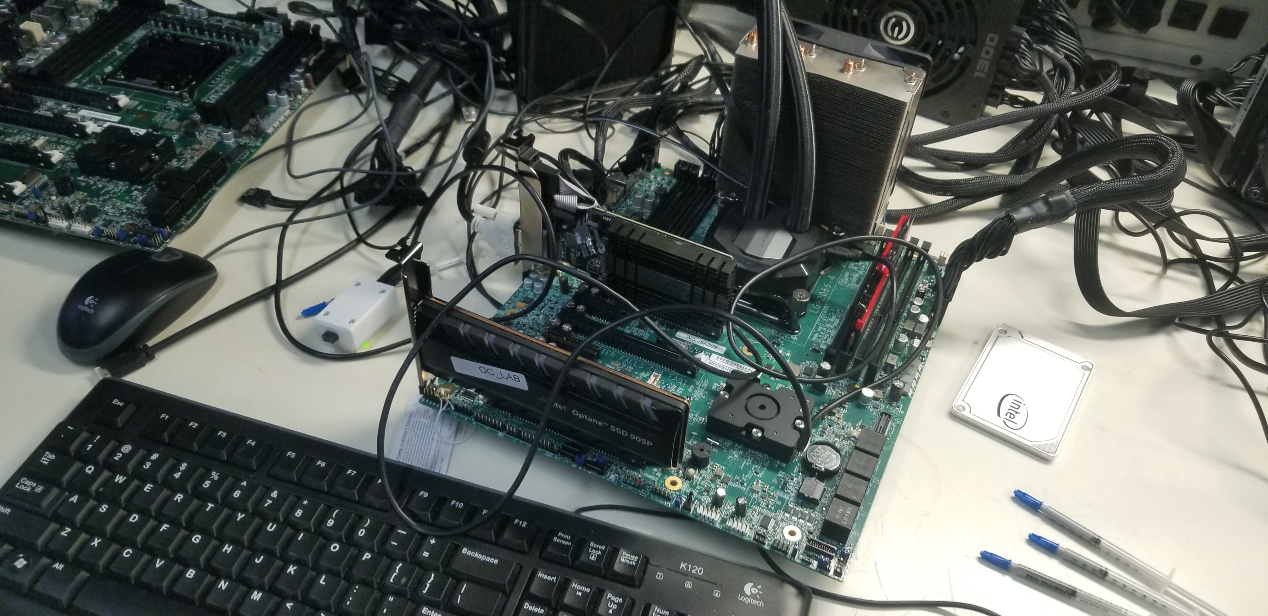
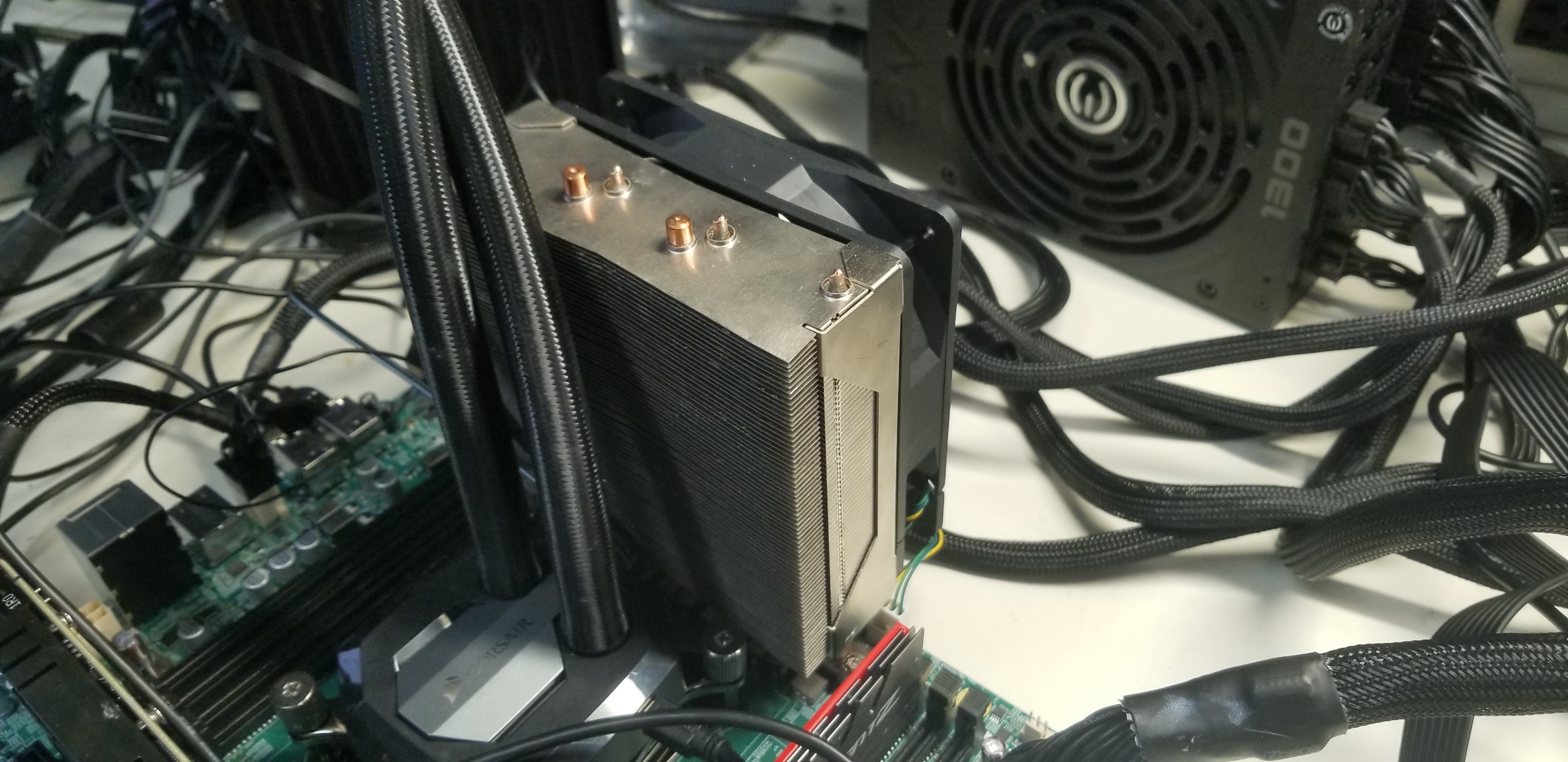
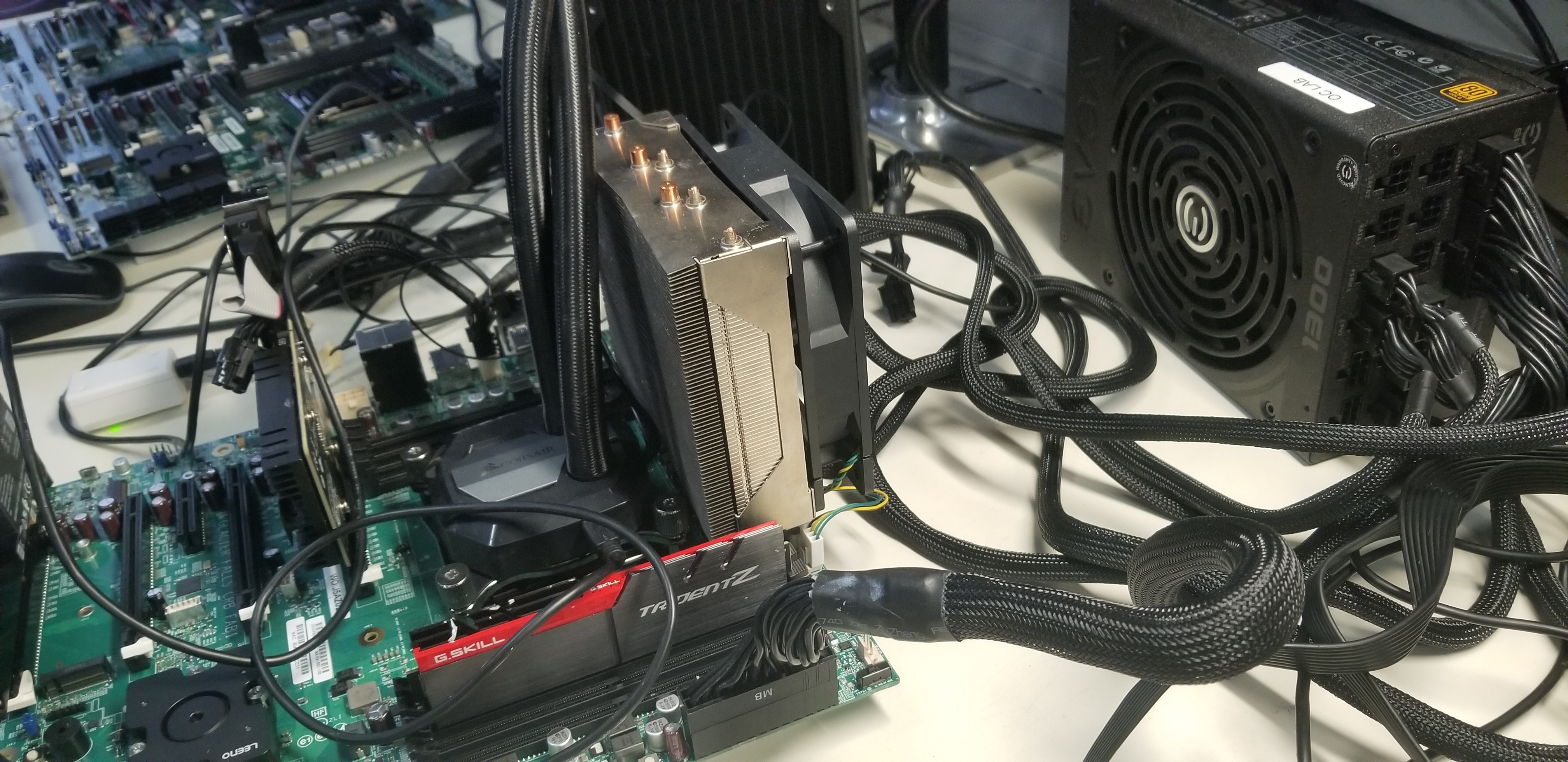
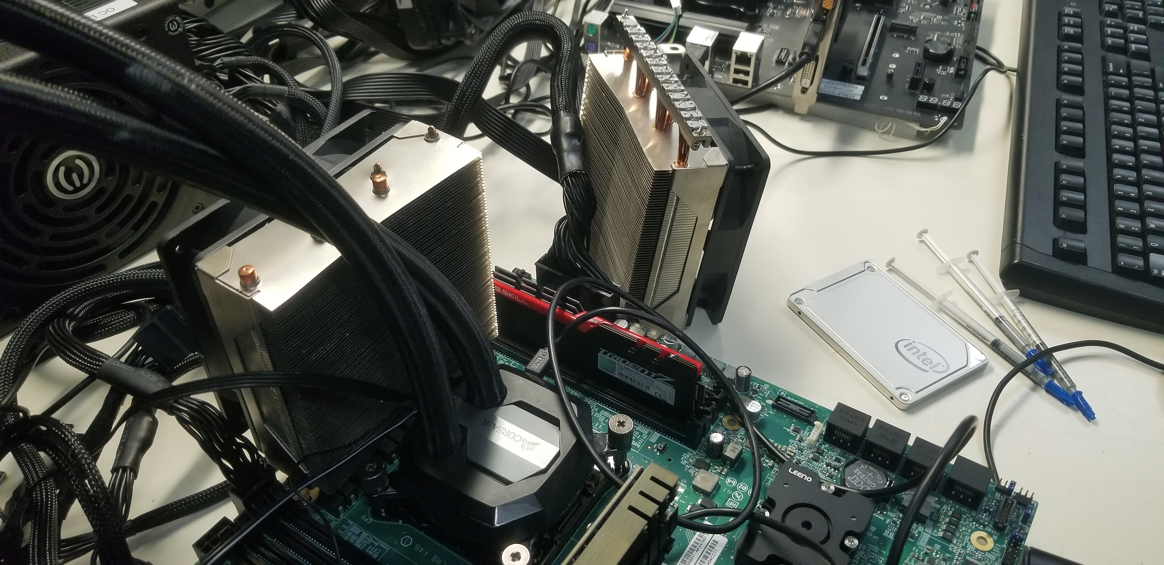
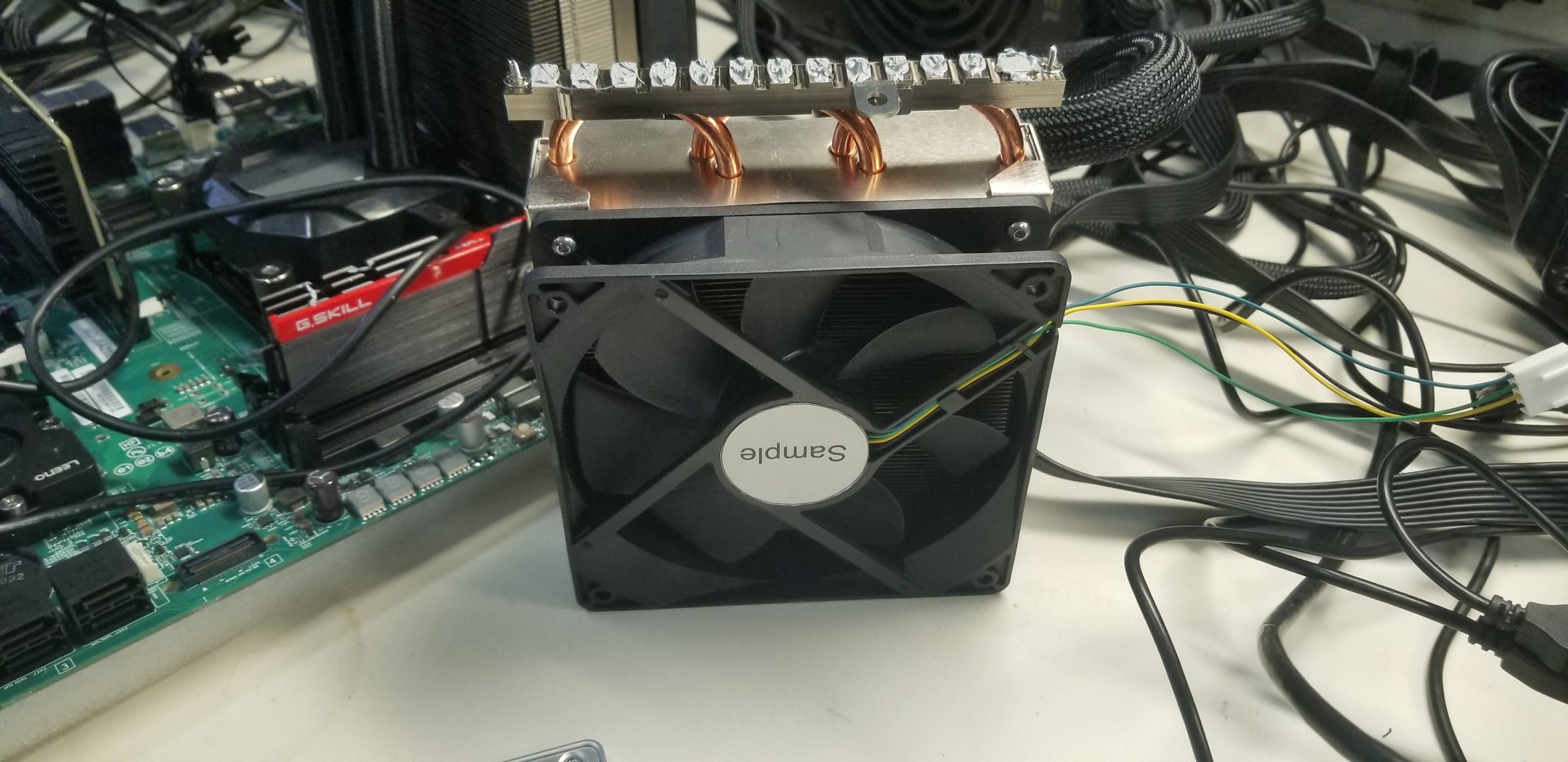
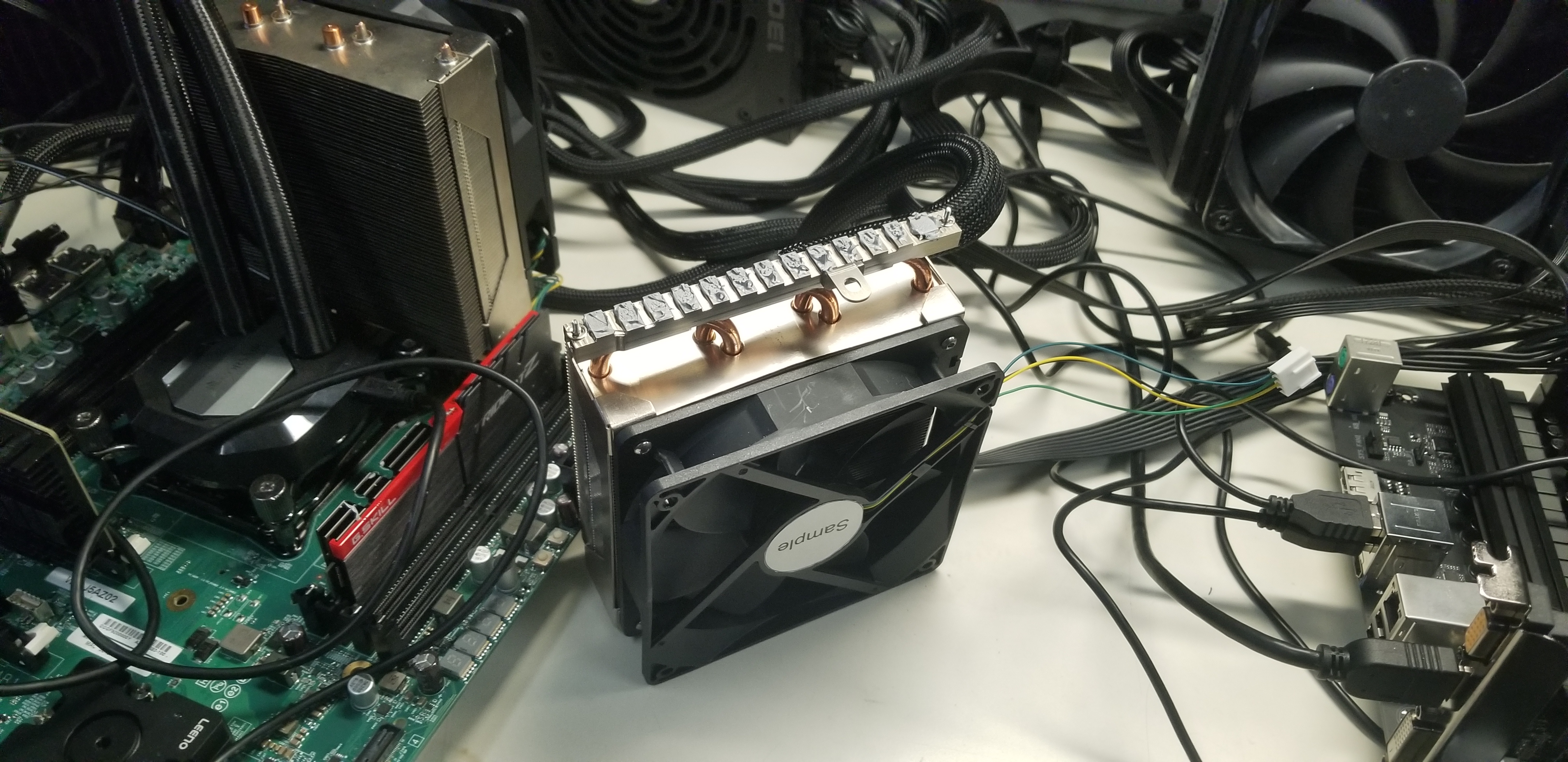
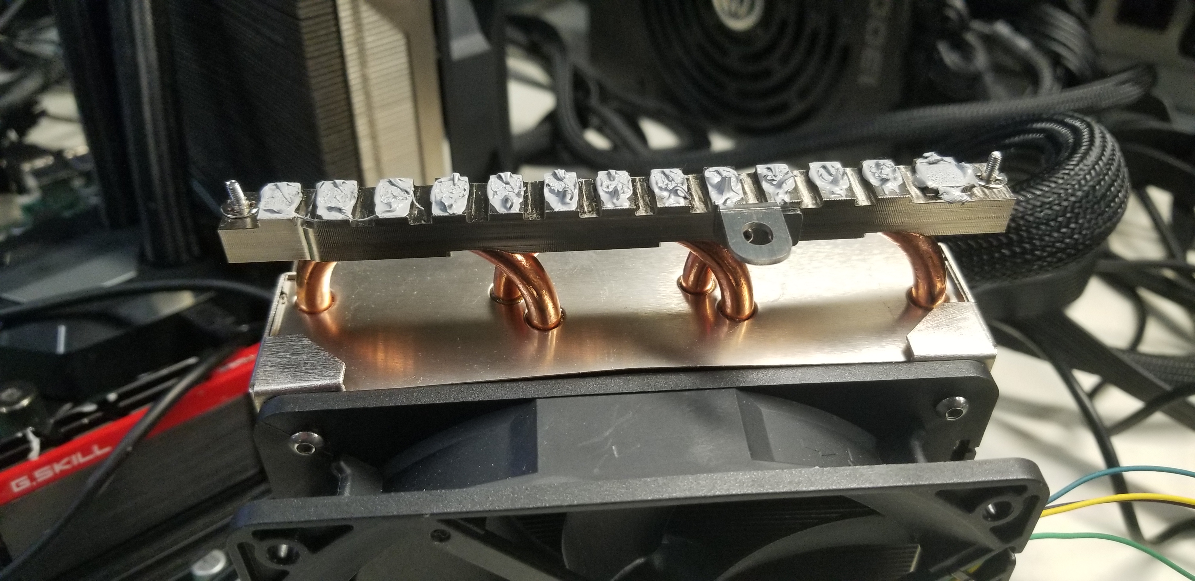
Here we can see the VRM cooling solution that Intel uses for its HEDT reference validation platform (RVP). After the issues we found with VRM cooling on Skylake-X motherboards, this certainly struck a chord.
Intel also ran into issues with VRM cooling while overclocking on its HEDT RVP (though the company didn't specify the exact generation of the chips under test), so the lab worked with its thermal engineering group to design a new heatsink (for internal use only) to address the issue. The lab pitched the project to its thermomechanical team, which includes a half-dozen PHDs, who then attacked the design with gusto. We're told that an amazing amount of design work and simulation went into the final heatsink design shown above. Unfortunately, there are only a few of these "insanely-overbuilt" heatsinks, and they are designed specifically for Intel's RVP boards.
On the topic of VRM cooling, Intel defines specs for chip power delivery but doesn't have a specific cooling recommendation for those subsystems. Instead, it's up to the motherboard vendors to assure that the cooling solutions meet the ratings of the various VRM componentry so it operates fully, particularly under high load during overclocking. While Intel doesn't set requirements for VRM cooling, they do test that as part of their normal flow with retail motherboards and give advice and feedback to the vendors.
Article continues belowHow to Swap Your PCH
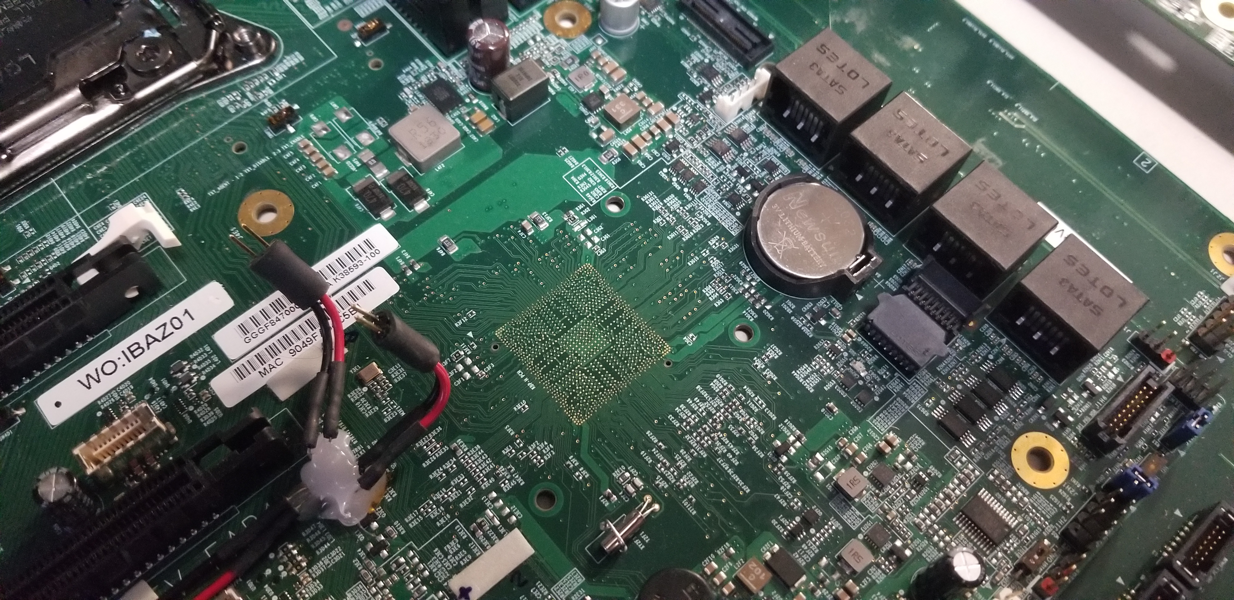
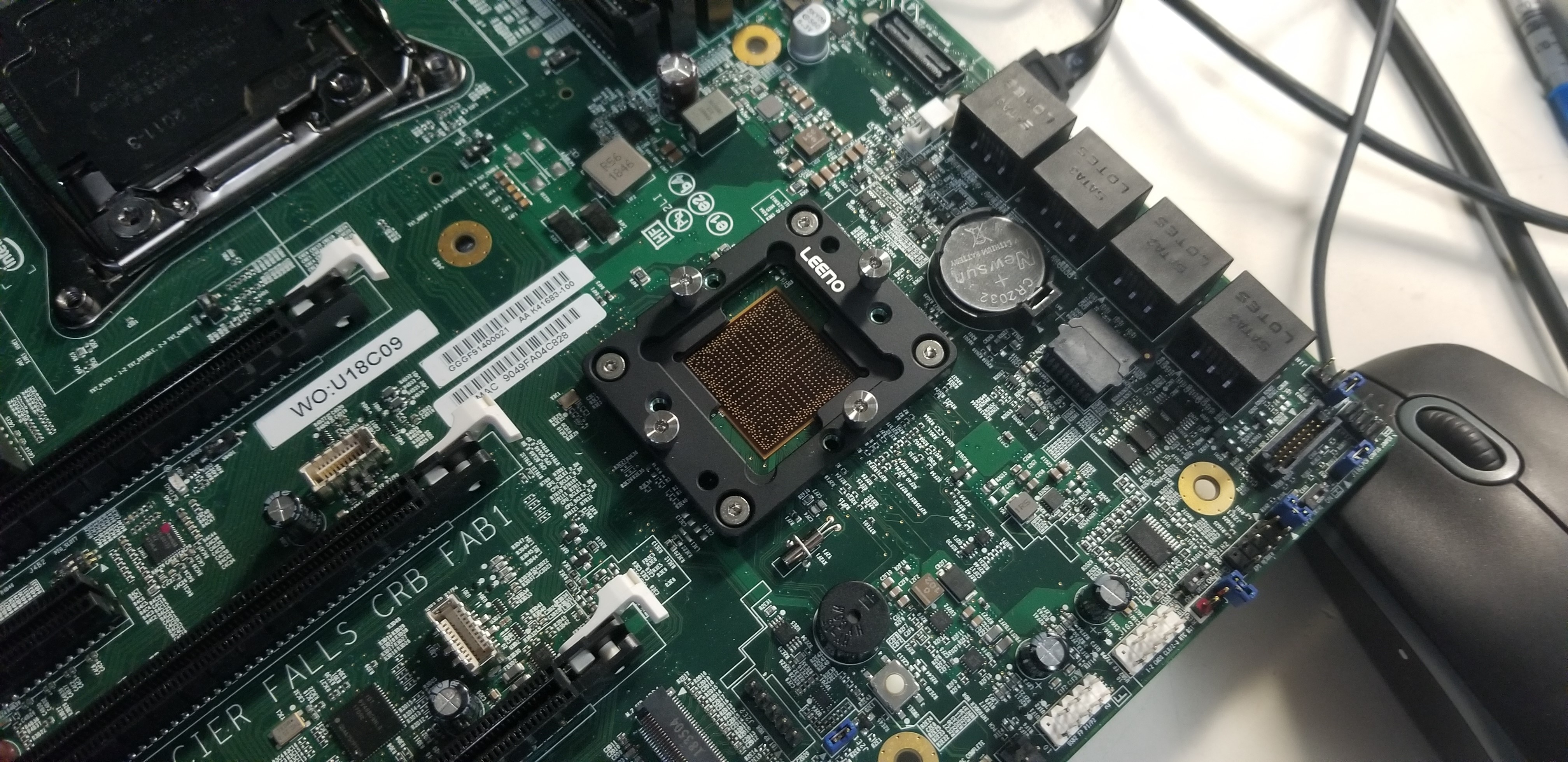
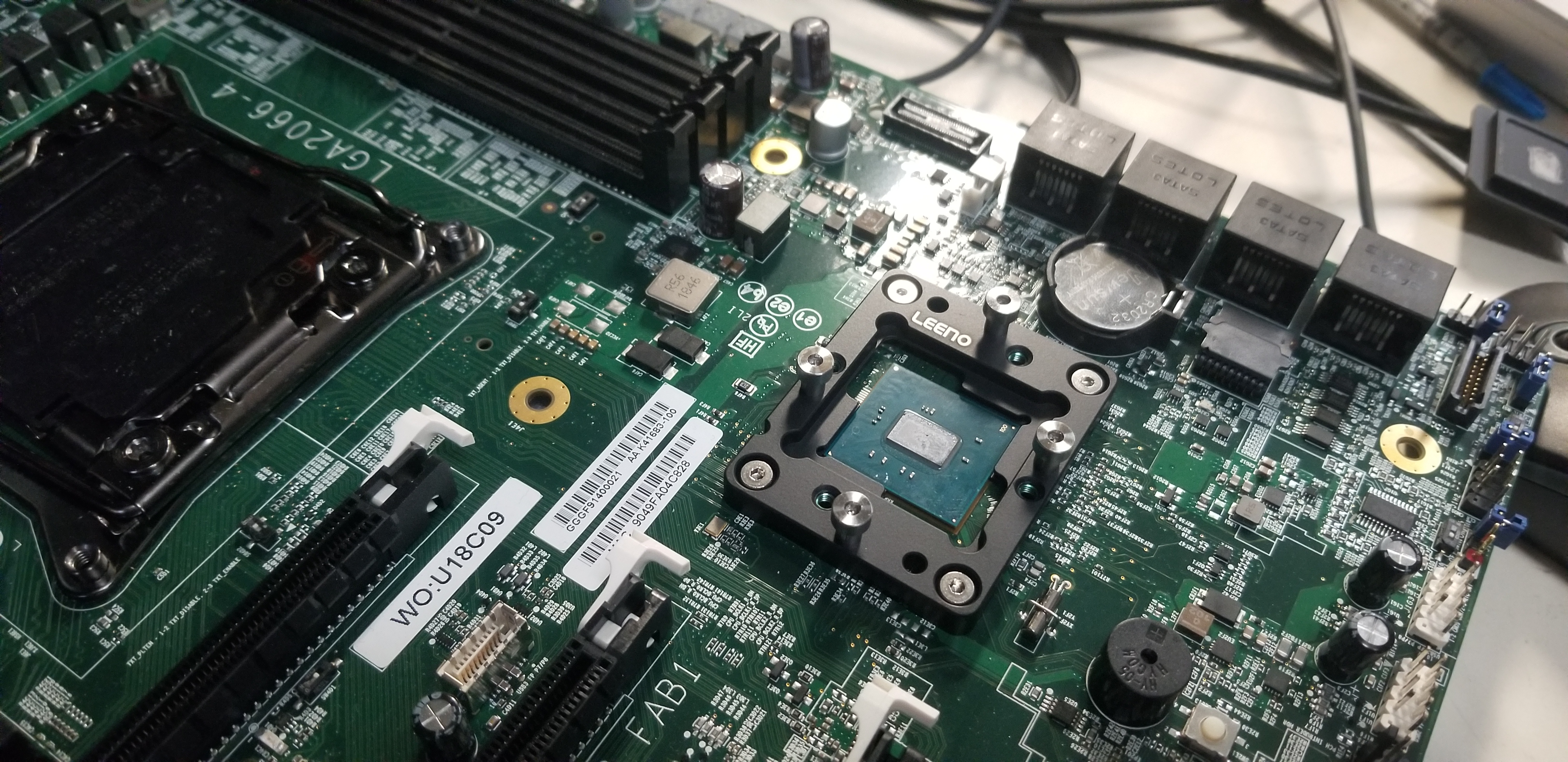
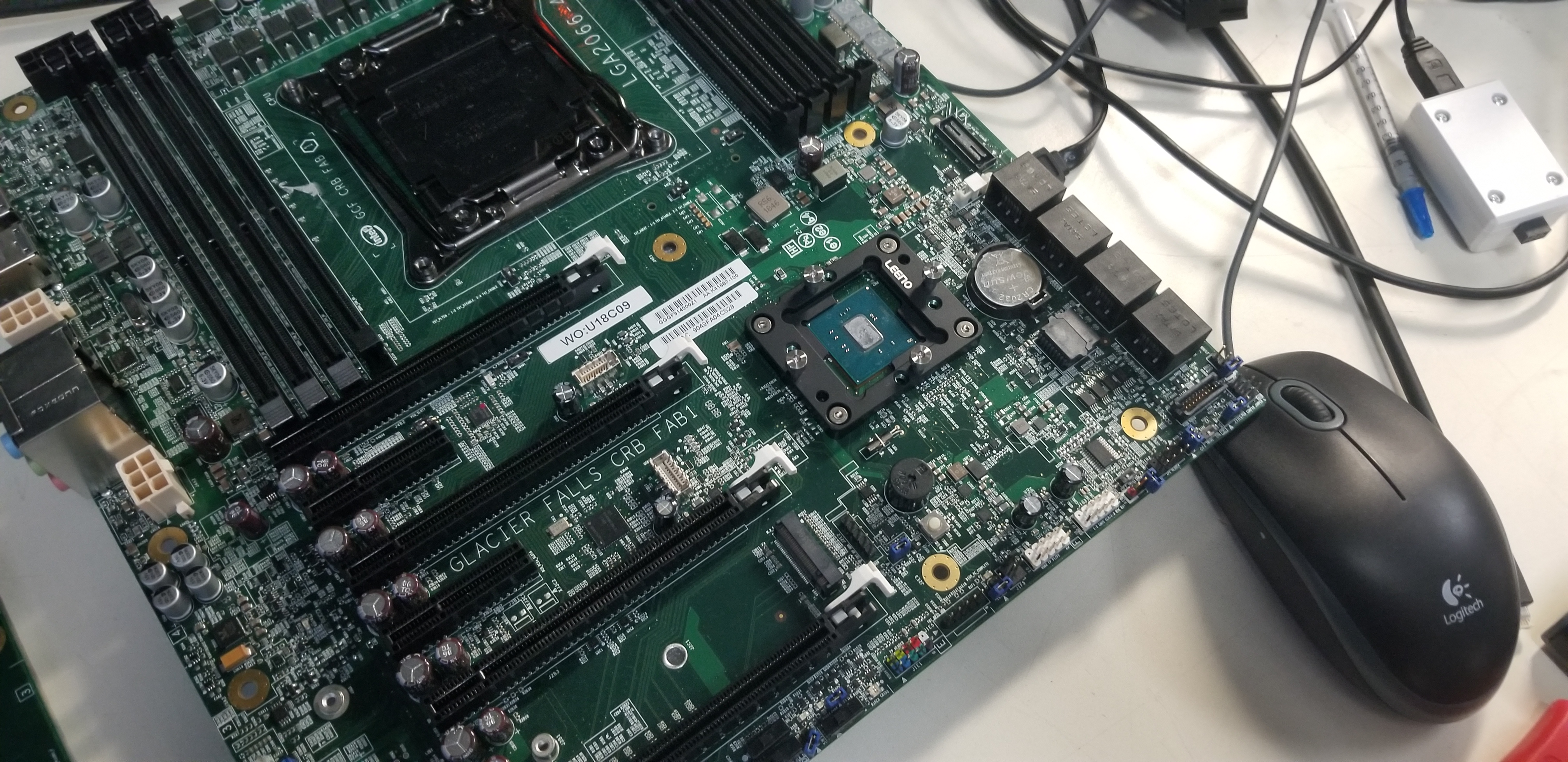
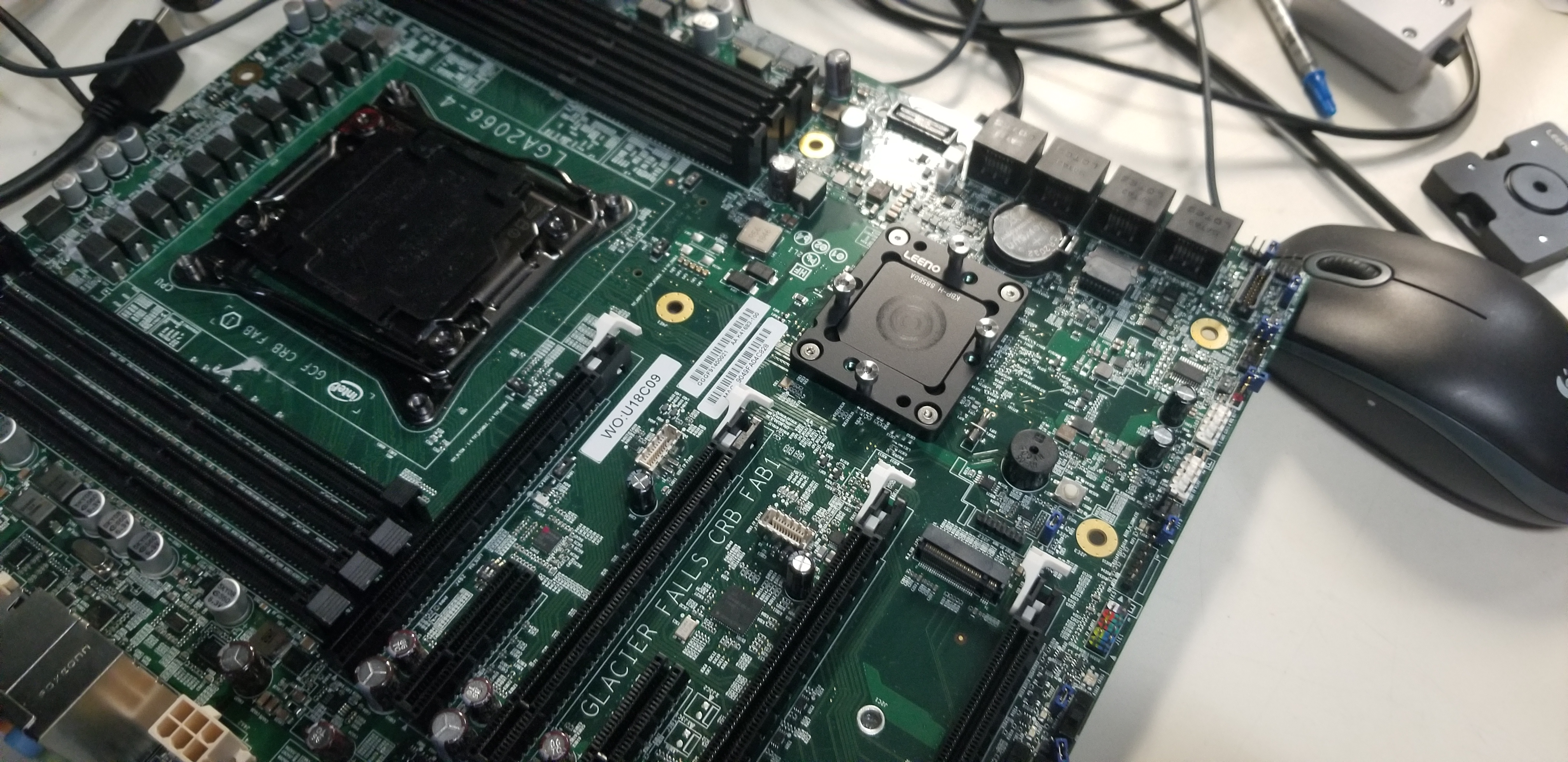
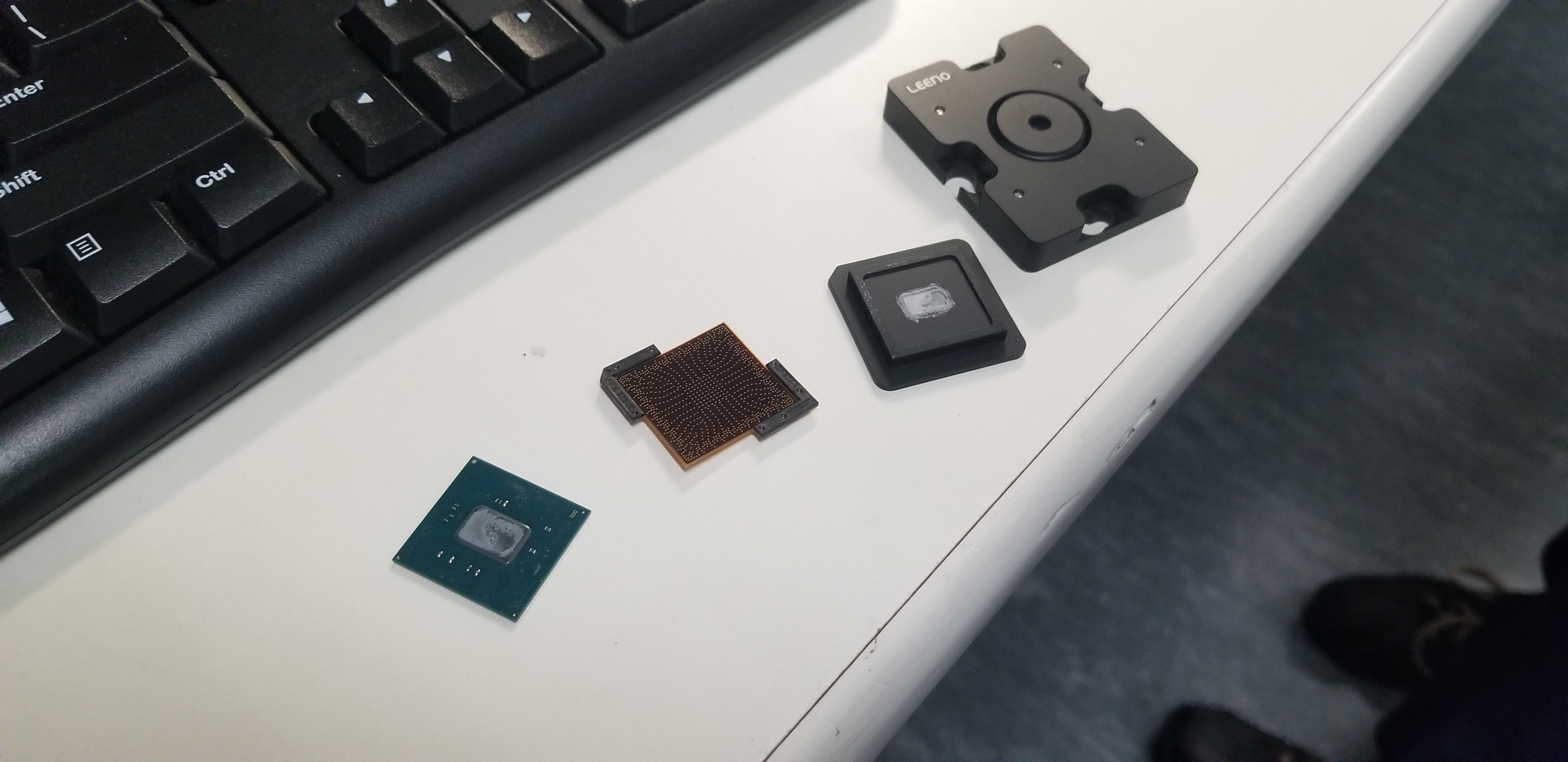
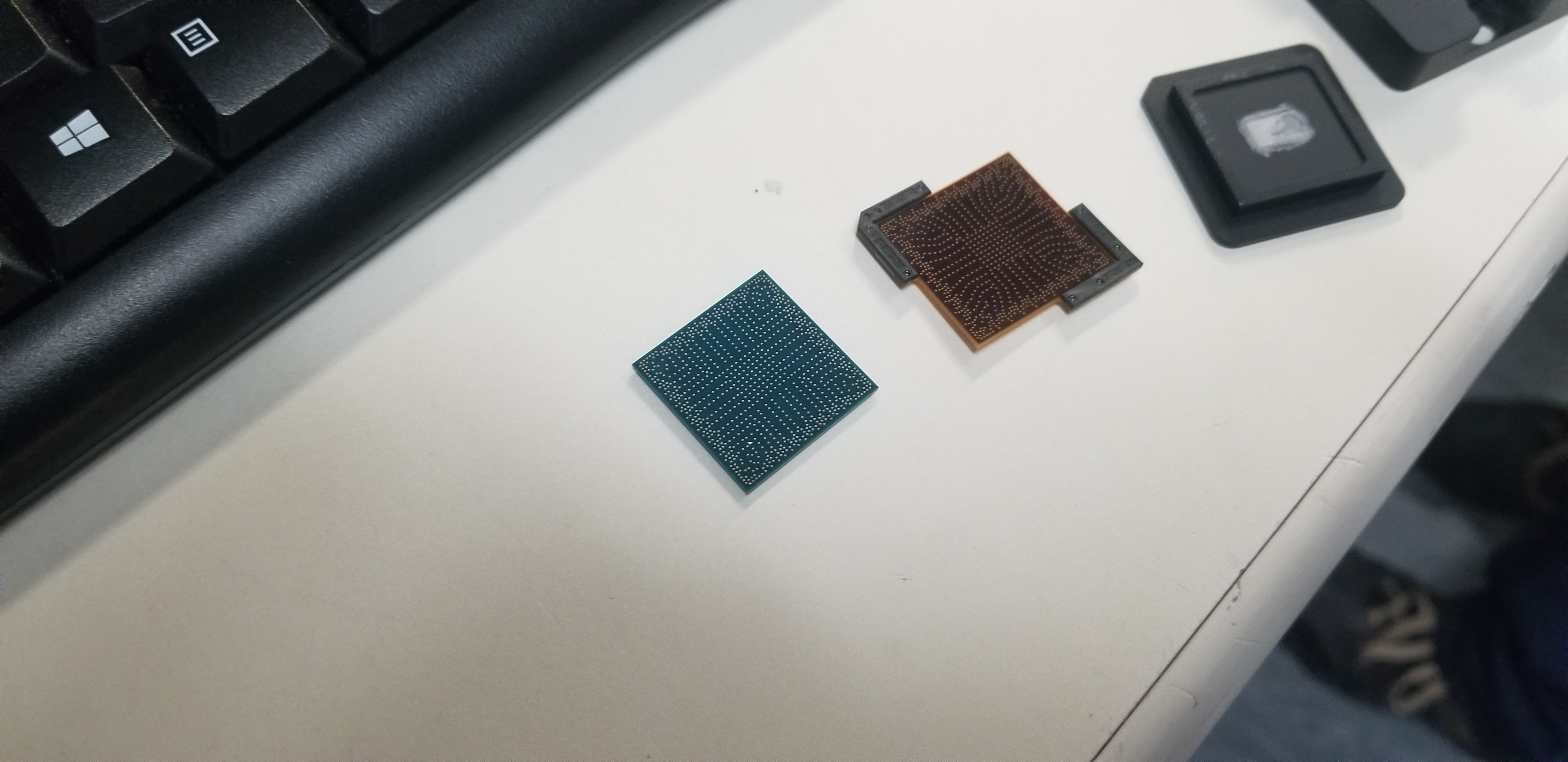
Intel's RVP boards have an interesting feature: sockets for platform controller hubs (PCH). For motherboards purchased at retail, these chips are soldered onto the board to provide the necessary I/O functions, but Intel's lab team has to test and validate multiple generations and new steppings of the various PCH chips during development. This socket allows for fast and flexible swapping of new PCH revisions.
These elastomer test sockets are fairly simple. The techs assemble the black retention mechanism around the bare BGA mounts on the motherboard, then drop in an interposer. These interposers are only rated for 15 insertions, though we're told they typically last much longer. The tech then drops the BGA PCH chip/substrate into the socket and tightens down the retention mechanism, which assures proper mating with the interposer and the underlying BGA pads on the motherboard. The housing provides enough thermal dissipation for the PCH, but Intel can also attach other cooling solutions to the top of the mounting mechanism if needed.
Intel Test Tools: XDP, XTU, PTU, TAT
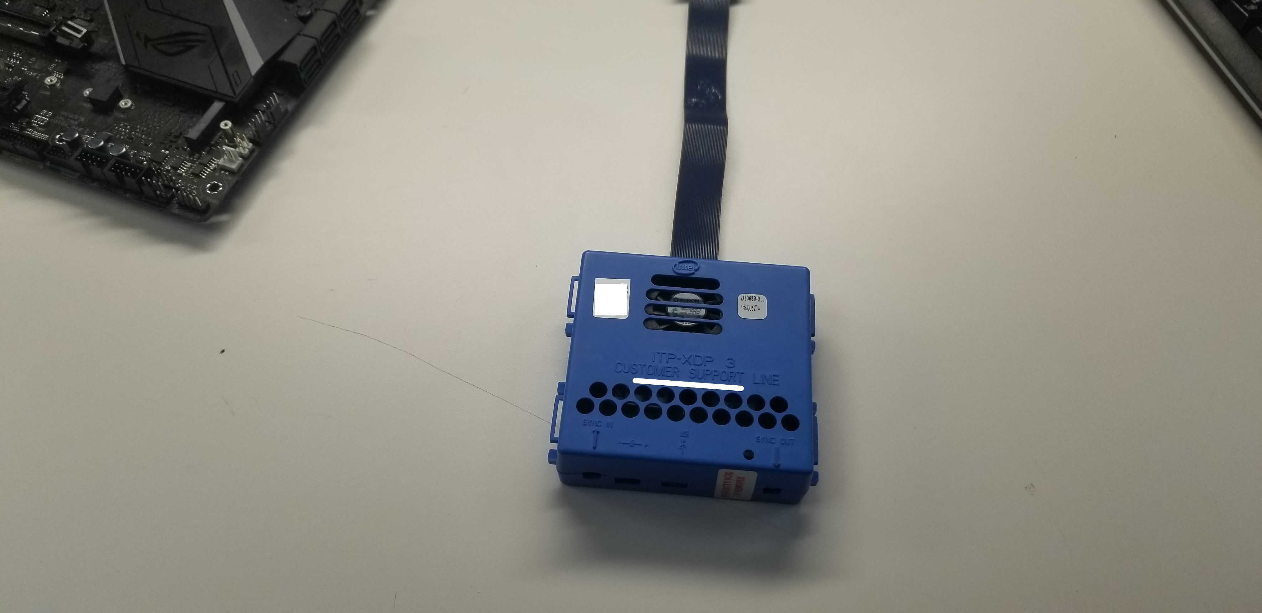
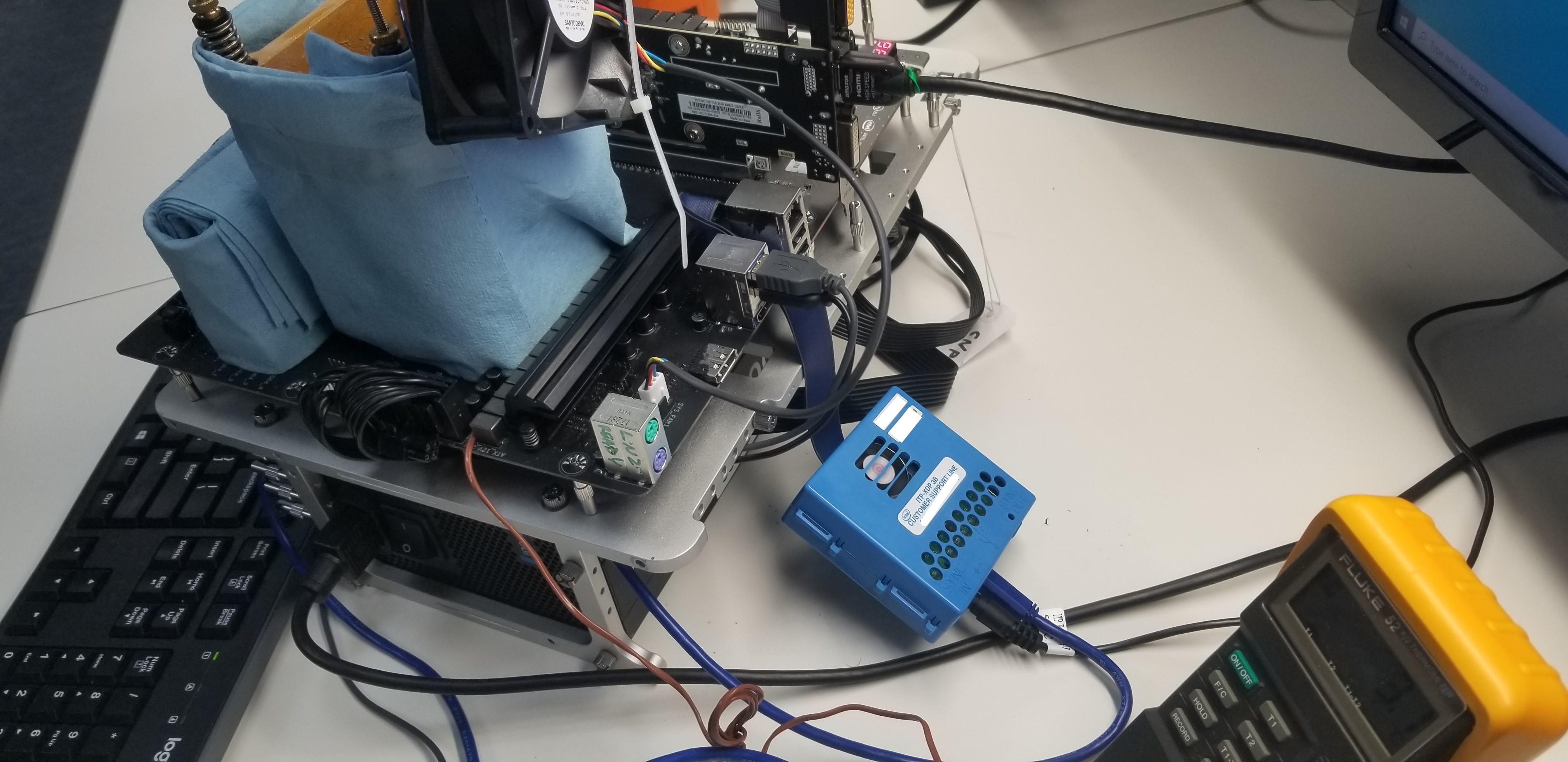
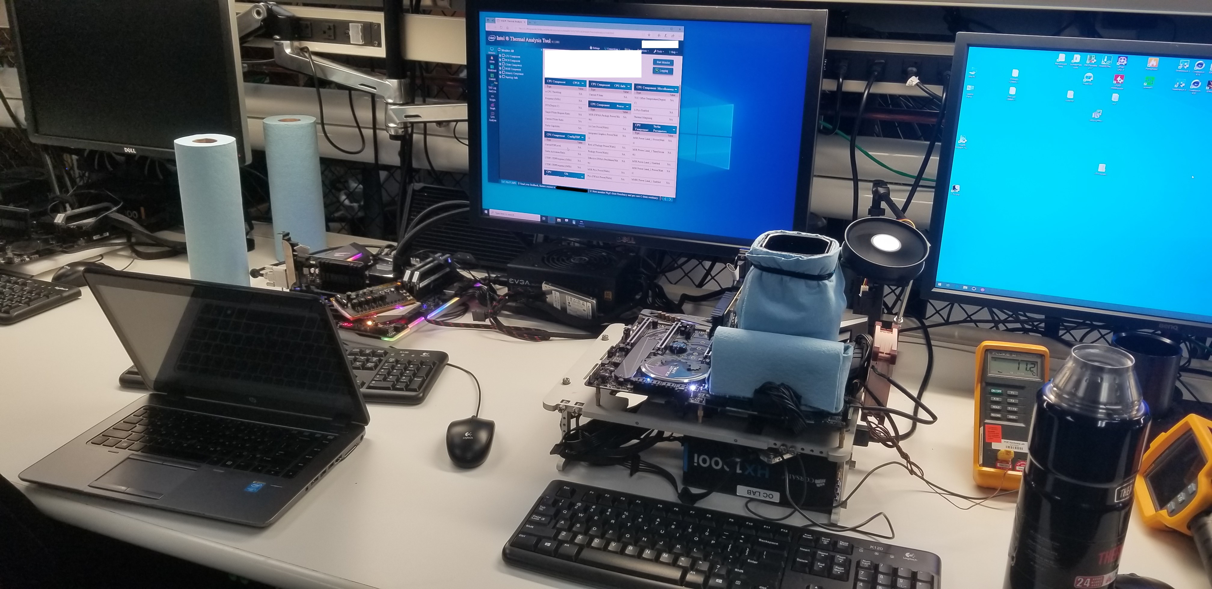
Our demos of Intel's internal testing tools were very informative, but the company is very guarded with details of some of its test tools, like the ITP-XDP box above, so we can't share screenshots, or even descriptions, of some of the interfaces. This is definitely among the most secret of Intel's tech in the lab, so there was quite a bit of trepidation from the lab team about exactly what they could show us, and what we could show you. After several clarifying conversations between the lab crew and the PR team assigned to our tour, and some negotiation on our part, the team allowed us to get at least a broad outline of this box and its capabilities.
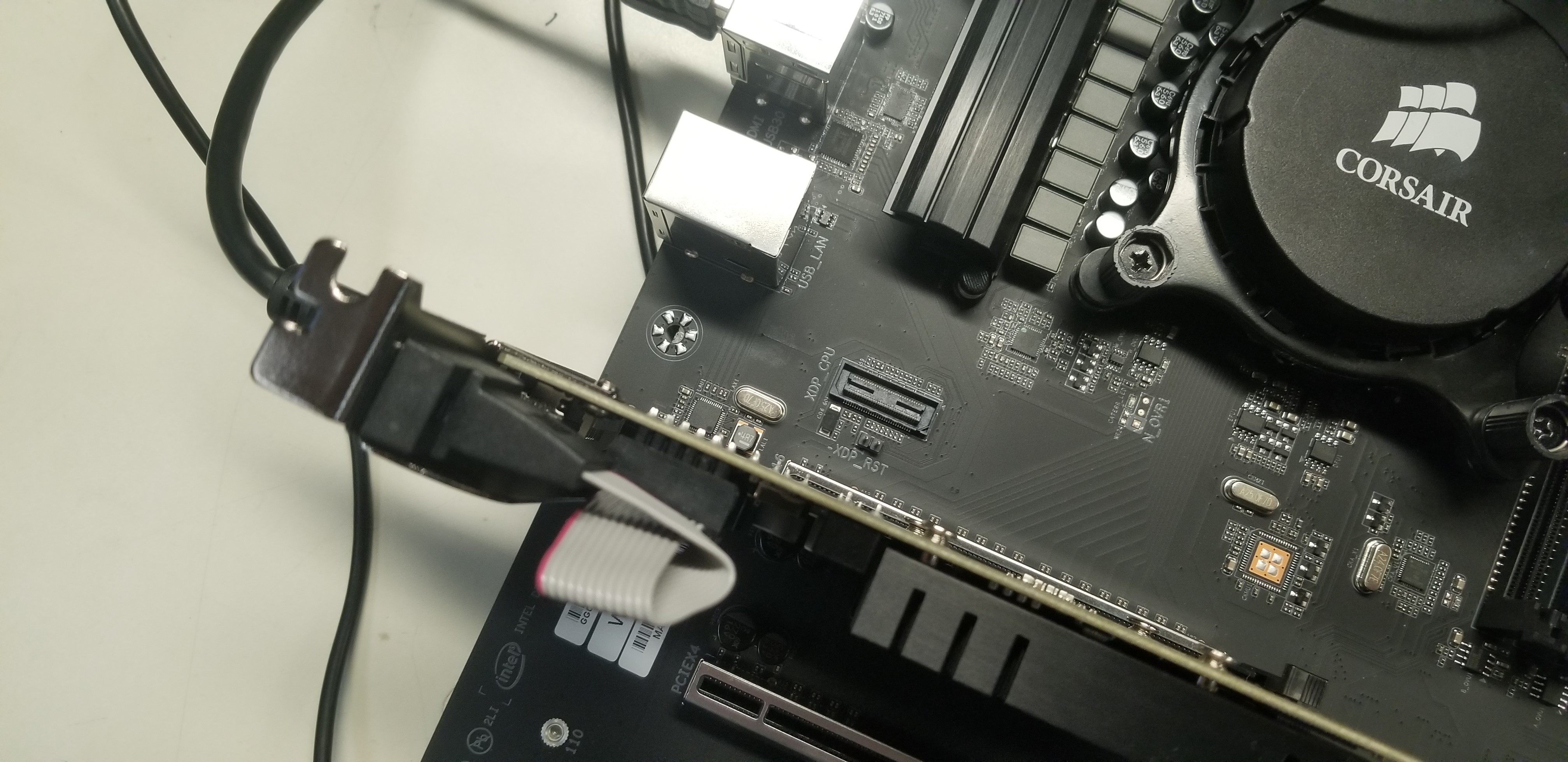
Intel's RVP platforms have an XDP socket (pictured above) that allows the company to have unprecedented insight and control of its chips in real-time.
Get Tom's Hardware's best news and in-depth reviews, straight to your inbox.
The company also provides ITP-XDP units to its ecosystem partners for their own testing and debug use, and motherboard vendors also add XDP ports to their test boards. Intel also has scripts that it allows the motherboard vendors to run on their hardware during its overclocking workshops. However, the Intel-proprietary box has multiple layers of security that assure a tiered access level, with only Intel having full access to the features. The final layer of security is so strictly controlled that Intel's OC lab technicians have to log each and every use of the unrestricted feature layer to a central database.
At the unrestricted access level, in the lab's own words, the ITP-XDP enables a connection to the chip that is "like having a direct connection to your brain." The ITP-XDP connects to a host system, which is then connected to the target (the system being observed/tested) and allows Intel to monitor and change internal parameters, MSRs, and literally every configurable option inside of a processor, in real-time. It doesn't just monitor the CPU, either: the interface also monitors every component connected to the chip.
This tool allows the team to identify overclocking bottlenecks and issues, and then change settings on the fly to circumvent those limitations. The lab then relays that information back to other relevant teams inside of Intel to optimize the processor design for overclocking.
The real-time changes, paired with exclusive hooks, unlock possibilities that Intel will never expose to normal users. For instance, theoretically, you could change cache timings and internal fabric settings in real-time after the operating system is running, among many other possibilities. This allows the chip to operate in ways that wouldn't make it past boot up. The lab engineers can overclock and test all the different parameters of the chip in ways that we won't ever have access to, which is probably part of the reason why they techs aren't allowed to submit HWBot world records. We're told world records fall easily with the capabilities enabled by the system.
Just for kicks, we requested a sample unit. The odds of that request being approved are somewhere south of zero.
Intel's overclocking team played an integral part in the development of the publically-available XTU software, and also works on the ongoing updates. The team designed the software to be useful, and they eat their own dog food. The team often uses the tool to test overclocking with settings that normal customers have access to.
Intel also has other restricted-use software utilities, like the power/thermal utility (PTU) that we've tested with a few times (as we did here), and the thermal analysis tool (TAT), which is used to monitor and diagnose conditions that impact boost activity. The latter utility is incredibly useful for diagnosing problems associated with boosting activity, and because overclocking really boils down to running in a heightened boost state, it also proves useful for debugging OC issues, like which internal power limits are restricting higher clock speeds. Intel uses these utilities heavily, but also provides them to motherboard vendors for qualification work.
- PAGE 1: The Overclocking Lab
- PAGE 2: The Beginnings and Mission of Intel's Overclocking Lab
- PAGE 3: Pouring LN2, the OSHA Way
- PAGE 4: TIM, Coolers, The Medusa, and Other Intel Lab Gear
- PAGE 5: Validation Boards and Overclocking Bootcamps
- PAGE 6: VRM Supercooling, PCH Swapping, and Internal Tools
- PAGE 7: 'Safe' Overclocking Voltages and Techniques
- PAGE 8: Is Overclocking Dead?
MORE: Best CPUs
MORE: Intel & AMD Processor Hierarchy
MORE: All CPUs Content
Current page: VRM Supercooling, PCH Swapping, and Internal Tools
Prev Page Validation Boards and Overclocking Bootcamps Next Page 'Safe' Overclocking Voltages and Techniques
Paul Alcorn is the Editor-in-Chief for Tom's Hardware US. He also writes news and reviews on CPUs, storage, and enterprise hardware.
-
Paul Alcorn ReplyDark Lord of Tech said:Can you get the AMD tour? Would love to see that.
I'll jump on a plane the second it is offered :) -
bit_user @PaulAlcorn , thanks for the awesome piece!Reply
I'm still making my way through it, but wanted to draw special attention to this bit:
the engineers told us they feel perfectly fine running thier Coffee Lake chips at home at 1.4V with conventional cooling, which is higher than the 1.35V we typically recommend as the 'safe' ceiling in our reviews. For Skylake-X, the team says they run their personal machines anywhere from 1.4V to 1.425V if they can keep it cool enough, with the latter portion of the statement being strongly emphasized.
Thanks for that!
At home, the lab engineers consider a load temperature above 80C to be a red alert, meaning that's the no-fly zone, but temps that remain steady in the mid-70’s are considered safe. The team also strongly recommends using adaptive voltage targets for overclocking and leaving C-States enabled. Not to mention using AVX offsets to keep temperatures in check during AVX-heavy workloads. -
StewartHH Some one should comparison between different vendors die size like Intel 10nm vs AMD 7nm to see if there is actually performance gain. I would use per-core speed and not taking multiple cores into account.Reply -
bit_user @PaulAlcorn , uh oh. Now that I just finished heaping praise, I've got a gripe. In the penultimate paragraph:Reply
... assures that the learnings lessons and advances made in the overclocking realm ...
I was saddened to see the "learnings" virus infecting your otherwise admirable writing.
I think "learnings" is one of those pseudo-jargon words that MBAs and other B-school types like to throw around, out of jealousy for practitioners of real professions. Everyone from auto mechanics to accountants, lawyers, and doctors needs jargon to adequately and efficiently express concepts and constructs central to their work. However, common sense pervades business to such a degree that I think they're embarrassed by how easily understandable it'd be, if they didn't inject some fake jargon to obscure the obvious. The resulting assault on the English language is disheartening, at best.
Yes, if you've ever heard of her, you probably guessed I'm a fan of Lucy Kellaway, former journalist of the Financial Times and BBC. Worth a read:
The 8 Lucy Kellaway rules for claptrap and the fundamental theorem of corporate BS
Lucy Kellaway’s dictionary of business jargon and corporate nonsense -
Gurg AMD CTO Mark Papermaster: "you can't rely on that frequency bump from every new semiconductor node." AMD's future outlook of very limited frequency bumps, performance increases only from more cores and expensive software modifications to use more cores.Reply
VersusIntel Ragland: "People who think this the end of the world for overclocking because our competitors' 7nm has very little headroom, that's not true. Intel is all about rock-solid reliability; our parts aren't going to fail...you can count on your part running at spec, so there's so much inherent margin that we will always have overclocking headroom...I think users will be happy with the margin we can offer in the future."
Ouch! Intel's Ragland really "punked" AMD's negative outlook.
PS Great fascinating article -
jiang-v Anyone knows how to made contact with them? cause I fould a big bug on 10th corex chip about adaptive mode overclockingReply
overclocking/comments/ehxa7cView: https://www.reddit.com/r/overclocking/comments/ehxa7c/big_bug_in_10th_core_x_vid_mechanism_worst_avx512/ -
nofanneeded In the past OC gave a huge difference , today we can easy hit 4.4 all cores without OC and this is more than enough for me.Reply
for me OCing is dead. and I dont care about missing 5 fps.
I put the price difference in a better GPU ... -
CompuTronix Outstanding article! Thank you, Paul! I would love to have been there. I have a few dozen questions that the Team may or may not have been allowed answered.Reply
However, like bit_user, I found it of particular interest that the Team was forthcoming regarding specific voltage and temperature values they're comfortable with running on their personal home rigs, which max out at 1.425 and 80°C. With respect to electomigation and longevity, every day in the forums we see many overclockers express their concerns over these very issues.
On their website, Silicon Lottery shows Historical Binning Statistics that include the Core voltages used to validate their overclocked 14 and 22nm processors. For 22nm the maximum is 1.360. For 14nm the maximum is 1.456. While Intel's warranty is 3 years, Silicon Lottery's warranty is 1 year, which suggests at least one reason for the voltage difference between Intel's Team and Silicon Lottery.
Here's a forgotten link to a revealing Tom's Hardware video interview of July, 2016, with Intel's Principal Engineer (Client Computing Group), Paul Zagacki, where BGTnJkuqlbo']Intel Discusses i7-4790K Core Temperatures and Overclocking. The video coincides with the formation of Intel's Overclocking Lab, also in 2016. In the video, Intel points out that overclocking abilities begin to "roll off" above 80°C, which agrees with the value the Team revealed in your article.
While Core temperatures, overclocking and Vcore are often highly controversial and hotly debated topics in at least the overclocking forums, the term "electromigration" is closely related to a much less known term, which is "Vt (Voltage threshold) Shift". With respect to voltage and temperature, the two terms describe the causes and effects of processor and transistor "degradation" at the atomic level.
In the Intel Temperature Guide, in Section 8 - Overclocking and Voltage, I created a table for Maximum Recommended Vcore per microarchitecture from 2006 to the present. For 22 and 14nm, those values are 1.300 and 1.400 respectively. I also created a graph showing the Degradation Curves for 22 and 14nm processors. The table and graph helps overclockers get a better perspective of the degradation and longevity issue:
Sparing our members and visiting readers the deep dive, Vt Shift basically represents the potential for permanent loss of normal transistor performance. Excessively high Core voltage drives excessively high current, power consumption and Core temperatures, all of which contribute to gradual Vt Shift over time. Core voltages that impose high Vt Shift values are not recommended. The 14nm curve suggest 1.425'ish is the practical limit, which also agrees with the value the Team revealed in your article. The curve also suggests that Silicon Lottery might be pushing the edge of the envelope a bit.
The concern here is that when novice overclockers casually glance around the computer tech forums, where conflicting and misleading numbers get flung around like gorilla poo in a cage, many don't realize through the fog of all the confusion that one size Vcore does not fit all. Aside from high Core temperatures, Vcore that might be reasonable for one microarchitecture can degrade another. So 22nm Haswell users now wanting to overclock their aging processors to keep up with today's games need to heed the degradation curves, which applies as well to 14nm Skylake and Kaby Lake users.
CT :sol: