Intel details 14A performance and new 'Turbo Cells' that unlock maximum CPU and GPU frequency

Turbo Cells
(Image credit: Tom's Hardware)

Intel made a slew of announcements at its Intel Foundry Direct 2025 event in San Jose, California, and finally shared performance metrics for its upcoming 14A process node, slated for risk production in 2027, touting headline improvements of up to a 35% reduction in power consumption. Intel also teased its new Turbo Cell technology, a customizable design approach geared to provide maximum CPU frequency and to boost performance for critical speed paths in GPUs.

The 14A and 14A-E nodes are the next generation after the company's 18A node. Intel says 14A will deliver a 15 to 20% performance-per-watt increase over 18A, which can be leveraged as either higher clock speeds or 25-35% lower power consumption at the same performance, depending upon chip-specific tuning. Much of this improvement is due to Intel's new direct-contact backside power delivery network, which the company has dubbed PowerDirect (more here).

Intel has also sprinkled in other new features to improve the node, such as a wider threshold voltage (Vt) range that enables a more expansive voltage/frequency curve.

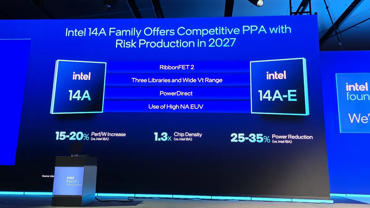
The 14A nodes also deliver a 1.3X increase in transistor density over the 18A node. Intel has also revamped its RibbonFET transistors for 14A, now known as 'RibbonFET 2.' Intel hasn't shared details about the new generation of RibbonFET, but the general design provides improved transistor density and faster transistor switching by utilizing four stacked nanosheets surrounded entirely by the gate (you can see the cross-section with nmos and pmos transistors above).

Turbo Cells and Critical Paths

Intel's new Turbo Cells are a standout feature, but they are a bit complicated. Turbo Cells can be used for a multitude of purposes, but Intel specifically calls out that they will be utilized in the critical paths of the CPU and GPU, often referred to as speed paths. And for good reason.

Timing paths within a processor are routes that a signal travels along, through wires and logic gates, during normal operation. However, delays to those signals can interrupt the clock timing of the processor. The critical paths are those that have the longest total delay.

Because processors operate based on clock signals, the slowest critical path dictates the highest possible frequency limit of the entire chip, serving as a bottleneck to overall performance (there are distinctions here for the various clock domains, but the general principle holds true). Chip designers often use higher-speed transistors in these areas of a chip, but this comes at the cost of reduced transistor density and increased power consumption, as faster transistors are leakier and thus consume more power. The new Turbo Cells provide chip architects with a more refined tool to mitigate critical paths.

The 14A node features three distinct standard cell libraries, which use process node-specific building blocks (standard cells constructed with transistors) of pre-designed logic gates and circuit elements. Designers use electronic design automation (EDA) software tools to utilize the libraries during the design flow and generally lay them out in rows.

Intel's 14A has three different libraries: the 'tall' library has transistor cells optimized for high frequency (low density, leaky), the 'mid-size' library is optimized for performance per watt, and the 'short' library is focused on density for area- and power-sensitive applications. Intel has not shared density information for the various libraries yet.

Short libraries are used heavily in CPUs and GPUs to pack in the most transistors possible while keeping power density at manageable levels. That's where Intel's new Turbo Cells step in.

asdf

(Image credit: Tom's Hardware)

Turbo Cells are designed to enhance performance by increasing the transistor drive current for short libraries when they're used to create double-height libraries (the height of two standard rows), all while maintaining a high-density arrangement for optimal area efficiency.

The above graphic represents four different arrangements of nmos and pmos ribbons/nanosheets (pink and green) with varying widths and configurations to optimize drive current for different scenarios. The width of the ribbons can be adjusted, or they can be merged independently to create very wide ribbons for maximum drive current delivery. The various options provide designers with a robust toolkit for tailored implementations.

Intel says Turbo Cells can ultimately be used to mix in faster and less power-efficient cells with the power-efficient cells within the same design block to create the right balance of power, performance, and area (PPA) for any given use case.

Critical paths are the ultimate bottleneck; think of them as the weakest link in the chain. Intel's new Turbo Cells are designed to boost overall processor performance by speeding up those paths, but without making the compromises often used to solve the critical path problem. We'll have to wait until 2027 to see how that pans out.

Paul Alcorn
Managing Editor: News and Emerging Tech

Paul Alcorn is the Managing Editor: News and Emerging Tech for Tom's Hardware US. He also writes news and reviews on CPUs, storage, and enterprise hardware.

  • Findecanor
    Remember that "14A" is a trademark, not a measurement.
    Reply
  • TerryLaze
    Findecanor said:
    Remember that "14A" is a trademark, not a measurement.
    It is a marketing thing sure, but it is there to show that some progress was made, they also showed actual numbers. Or at least numbers, we will see when they come out if they are actual.
    30% density 15-20% per/W ,looks pretty good.
    https://cdn.mos.cms.futurecdn.net/JmiSB9VLmyq4HKsTz9memT-1200-80.png.webp
    Reply
  • rluker5
    Turbo cells seems like something they already should have had. Along with Power Direct to minimize EM interference.

    Getting stronger on the basics.
    Reply
  • Rob1C
    So, they plan on leaving the 6.2 GHz i9-14900KS in the dust?
    Reply
  • tennis2
    Chip design is amazing. How did humanity even get to this point at all?
    Reply
  • TheSecondPower
    rluker5 said:
    Turbo cells seems like something they already should have had. Along with Power Direct to minimize EM interference.

    Getting stronger on the basics.
    Power Direct is the second iteration of Intel's backside power delivery, and by this schedule will come to market about the same time as TSMC's first iteration of backside power delivery.
    Reply
  • bit_user
    rluker5 said:
    Turbo cells seems like something they already should have had.
    They already do things like this, with cells designed for different power/density tradeoffs. For a long time, IIUC.

    Another technique they've at least used in the past is to place multiple transistors in parallel, when necessary.
    https://www.anandtech.com/show/4818/counting-transistors-why-116b-and-995m-are-both-correct
    Reply
  • bit_user
    tennis2 said:
    Chip design is amazing. How did humanity even get to this point at all?
    Engineering involves a lot of iteration and progressive refinement. You figure out what are the limiting factors, focus on addressing those, and then re-analyze and probably find new limitations that need new solutions. All along the way, the process is fed by thousands of brilliant minds and many $B of investment. That's why some country can't just replicate all of that progress overnight, no matter what resources they throw at it.

    There's also something of a virtuous circle, where the machines produced by current technology enable us to design better machines tomorrow. Even with all the knowledge about how current chip manufacturing works, you couldn't just start turning out the same chips decades ago. Not only is there innovation along the entire supply chain, but also the sheer compute power needed to create photomasks for modern chips simply didn't exist very long ago. Not to mention place & route.
    Reply
  • bit_user
    Rob1C said:
    So, they plan on leaving the 6.2 GHz i9-14900KS in the dust?
    FWIW, the numbers quoted for performance & efficiency increases are usually based on a simple reference design. I think TSMC used an Arm Cortex-A7 core, for a long time. It's hard to predict exactly how they will translate into metrics of actual products made on these nodes.

    In the case of Arrow Lake, it seems like a big part of what held it back was the SoC architecture. So, even though the process node and microarchitecture were both substantially improved, those got kneecapped by a SoC design that prioritized other things above performance.
    Reply
  • JamesJones44
    tennis2 said:
    Chip design is amazing. How did humanity even get to this point at all?

    Time and investment. It's been almost 80 years since the transistor was invented and it's probably one of the most heavily invested in areas over that time. Time and money can drive a lot of refinement in a product. Even cars and airplanes are orders of magnitude more complex than they were 80 years ago thanks to heavy amounts of investment over that time.
    Reply