AMD's Ryzen 9 7950X3D is the fastest gaming CPU on the planet due to AMD's decision to bring its disruptive 3D chip-stacking tech to Zen 4, but curiously, the company didn’t share any details about its new Second-Gen 3D V-Cache in its Ryzen 7000X3D briefing materials. We initially found some details at a recent tech conference that we included in our review, and now AMD has finally answered a few of our follow-up questions and shared important new details, including that the chiplet remains on the 7nm process and now has a peak bandwidth of up to 2.5 TB/s, whereas the first-gen 3D V-Cache peaked at 2 TB/s (among lots of other new info). We also have new pics and diagrams of the new 6nm I/O Die that AMD uses for its Ryzen 7000 processors.
AMD has moved to the second-gen of its 3D V-Cache, and Intel doesn't have a competing tech. That assures AMD a win in both the best CPUs for gaming and certain data center applications. Overall, AMD's second-gen 3D V-Cache technology is an impressive step forward over the first-gen because it allows the company to leverage the now-mature and less-expensive 7nm process node to boost the performance of its cutting-edge 5nm compute die. The new design represents AMD taking the key advantage of chiplet-based design methodologies — using an older and less-expensive process node in tandem with expensive new process tech — into the third dimension. Now for the nitty-gritty details.


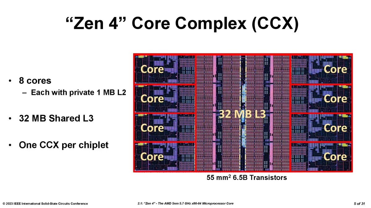
First, a quick high-level refresher. As you can see above, AMD’s 3D V-Cache tech stacks an additional L3 SRAM chiplet directly in the center of the compute die (CCD) chiplet to isolate it from the heat-generating cores. This cache boosts capacity to 96MB for the 3D V-Cache-equipped chiplet, thus boosting performance for latency-sensitive apps, like gaming. We’ve covered the deep-dive details of the first-gen of this technology here.
We received new information on the second-gen implementation both direct from AMD and from the 2023 International Solid-State Circuits Conference (ISSCC), where AMD made a presentation on the Zen 4 architecture.
AMD’s previous-gen 3D V-Cache used a 7nm L3 SRAM chiplet stacked atop a 7nm Zen 3 CCD. AMD stuck with the 7nm process for the new L3 SRAM chiplet (called 'L3D') but now stacks it on top of a smaller 5nm Zen 4 CCD (see the table below). This creates a size mismatch, though, which required a few alterations.
| Row 0 - Cell 0 | 2nd-Gen 7nm 3D V-Cache Die | First-Gen 7nm 3D V-Cache Die | 5nm Zen 4 Core Complex Die (CCD) | 7nm Zen 3 Core Complex Die (CCD) |
| Size | 36mm^2 | 41mm^2 | 66.3 mm^2 | 80.7mm^2 |
| Transistor Count | ~4.7 Billion | 4.7 Billion | 6.57 Billion | 4.15 Billion |
| MTr/mm^2 (Transistor Density) | ~130.6 Million | ~114.6 Million | ~99 Million | ~51.4 Million |
First, AMD made the 7nm SRAM die smaller, so it now measures 36mm2 compared to the previous-gen's 41mm2. However, the total number of transistors remains the same at ~4.7 billion, so the new die is significantly denser than the first-gen chiplet.
As we saw with the first-gen SRAM chiplet, the 7nm L3 SRAM chiplet has incredible transistor density — we're looking at almost 3x the density of the first-gen 7nm compute chiplet, and surprisingly, the 7nm SRAM chiplet is significantly denser than the 5nm compute chiplet. That's because, as before, the chiplet uses a density-optimized version of 7nm that's specialized for SRAM. It also lacks the typical control circuitry found in the cache — that circuitry resides on the base die, which also helps reduce latency overhead. In contrast, the 5nm die includes several types of transistors along with data paths and other types of structures not present in the simplified L3 SRAM chiplet.
As before, the extra latency from the additional L3 SRAM cache weighs in at 4 clocks, but the bandwidth between the L3 chiplet and the base die has increased to 2.5 TB/s, a 25% improvement over the previous 2 TB/s peak.
The stacked L3 SRAM chiplet is connected to the base die with two types of through-silicon vias (TSVs — a vertical electrical connection). The Power TSVs carry power between the chiplets, while the Signal TSVs carry data between the units.
In the first-gen design, both types of TSVs resided in the L3 region of the base chiplet. However, the L3 cache on the base die is now smaller due to the increased density of the 5nm process, and even though the 7nm L3 SRAM chiplet is smaller, it now overlaps the L2 cache (the prior gen only overlapped the L3 on the base die). As such, AMD had to alter the TSV connections in both the base die and the L3 SRAM chiplet.


AMD had to extend the power TSVs from L3 into the L2 region due to the smaller size of the 5nm L3 cache on the base die (a result of the increased density and other factors). For the base die, AMD achieved a 0.68x effective area scaling across the L3 cache, data paths, and control logic compared to the old 7nm base chiplet, so there is physically less room for TSVs in the L3 cache.
The signal TSVs remain inside the L3 cache area on the base die, but AMD shrunk the TSV area in the L3 cache by 50% by applying learnings from the first-gen design along with DTCO improvements to reduce overhead circuitry in the new interface design.
AMD's 3D chip stacking tech is based on TSMC's SoIC technology. TSMC's SoIC is bump-less, meaning it doesn't use microbumps or solder to connect the two dies. You can read much more about the hybrid bonding and manufacturing process here. AMD tells us it used the same fundamental bonding process paired with continued process and DTCO improvements, but the minimum TSV pitch hasn't changed.
| Tom's Hardware Measurements | Single-Threaded Peak | Multi-Threaded Sustained | Voltage (peak) | nT Power |
| CCD 0 (3D V-Cache) | 5.25 GHz | 4.85 GHz | 1.152 | 86W |
| CCD 1 (No extra cache) | 5.75 GHz | 5.3 GHz | 1.384 | 140W |
The L3 SRAM chiplet also remains on the same power domain as the CPU cores, so they can't be adjusted independently. This contributes to the lower frequency on the cache-equipped chiplet because the voltage can't exceed ~1.15V. You can see more in our in-depth testing of the two different types of chiplets here.


| Row 0 - Cell 0 | 6nm I/O Die (IOD) - Ryzen 7000 | 12nm I/O Die (IOD) - Ryzen 5000 | 6nm I/O Die (IOD) - EPYC |
| Size | 117.8mm^2 | 125mm^2 | 386.88mm^2 |
| Transistor Count | 3.37 Billion | 2.09 Billion | 11 billion |
| MTr/mm^2 (Transistor Density) | ~28.6 Million | ~16.7 Million | ~29.8 Million |
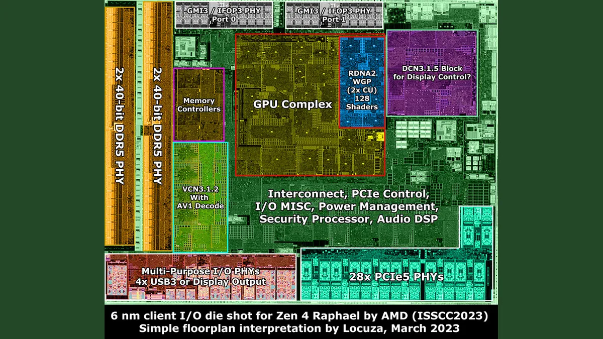
AMD's ISSCC presentation also included plenty of new details about the 6nm I/O Dies (IOD) used in the Ryzen 7000 and EPYC Genoa processors. In the above album, you can see the zoomed-in images and an annotated die shot from chip detective @Locuza_. You can also expand the tweet below to read Locuza's excellent analysis of the Ryzen 7000 IOD.
We put the specs in the table for easy comparison, and as you can see, the EPYC Genoa I/O Die is simply massive compared to the Ryzen 7000 variant — that's because AMD can wire up to 12 compute chiplets (CCDs) to the I/O Die for its EPYC Genoa processors.
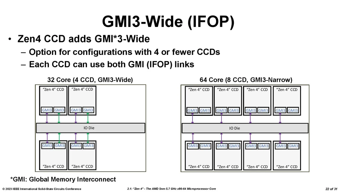
In contrast, the consumer chips are limited to two chiplets, an immutable limitation because, as you can see in Locuza's diagram, the Ryzen 7000 I/O Die only has two Global Memory Interconnect 2 (GMI2) links that connect the compute chiplets to the IOD. That's a bummer — this means the IOD will not support three compute chiplets. Additionally, lower core-count Genoa models with four CCDs can have dual-GMI3 links (wide mode), a new capability that can offer advantages in some memory throughput-intensive tasks. That would've been interesting to add to the dual-CCD consumer chips.
We've also added the full ISSCC 2022 deck below for your perusal — it includes a few other interesting tidbits.
Zen 4 Raphael 6 nm client I/O die:- 128b DDR5 PHY + 32b for ECC (8b per 32b channel)- 2x GMI3 Ports, 3x CCDs are not possible. :p- 28x PCIe 5, Zen1/2/3 cIOD had 32x PCIe lanes. So AMD reduced the waste for the client market. - Really just one RDNA2 WGP, 128 Shader "Cores" https://t.co/bkqdVvhgrn pic.twitter.com/erYxTw1p8hMarch 4, 2023