AMD Unveils More Ryzen 3D Packaging and V-Cache Details at Hot Chips
Stacking the chips
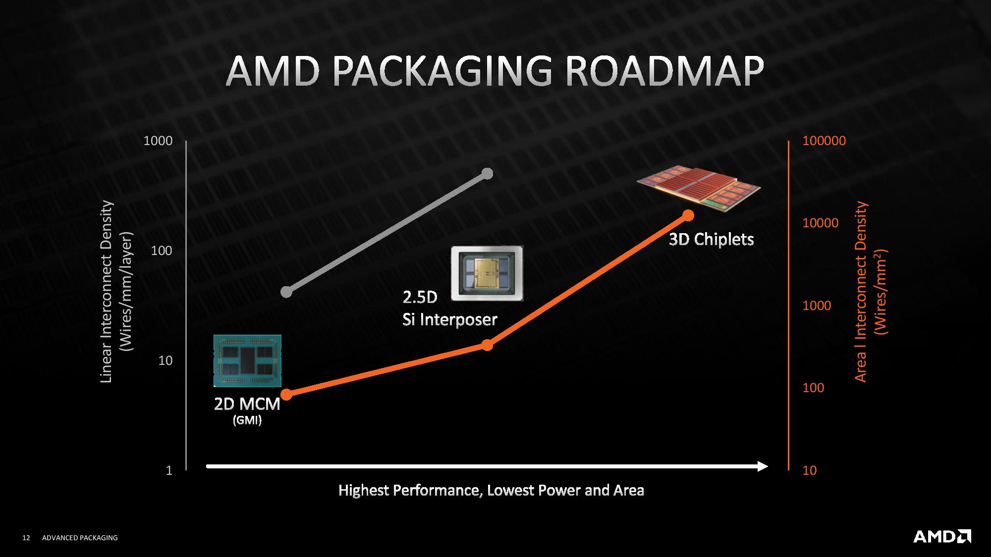
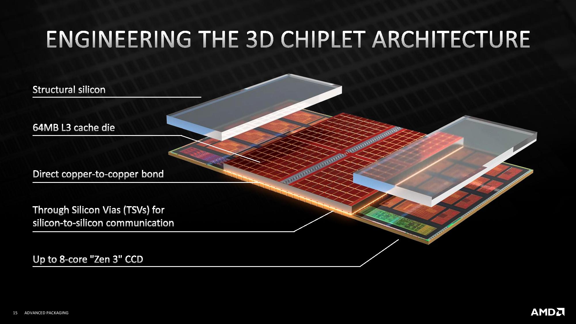
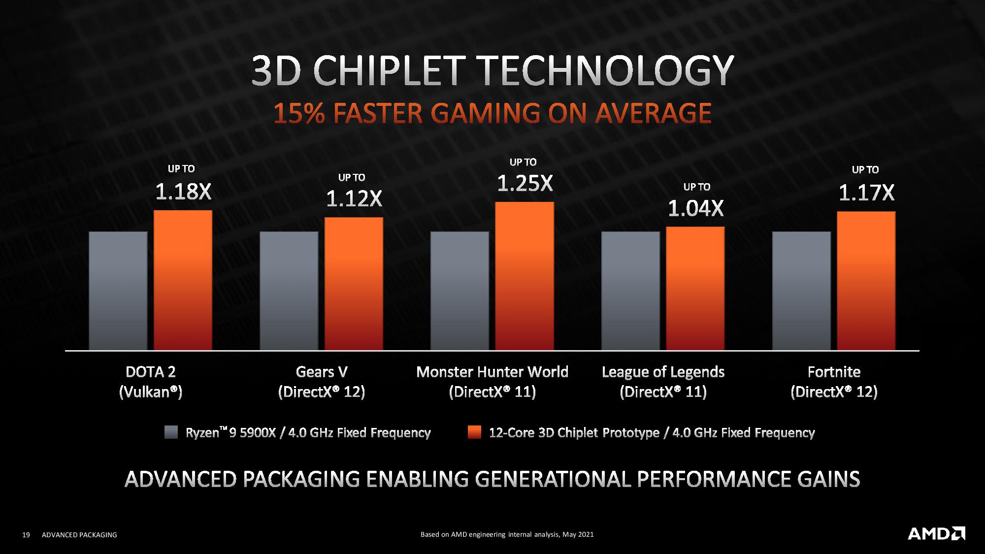
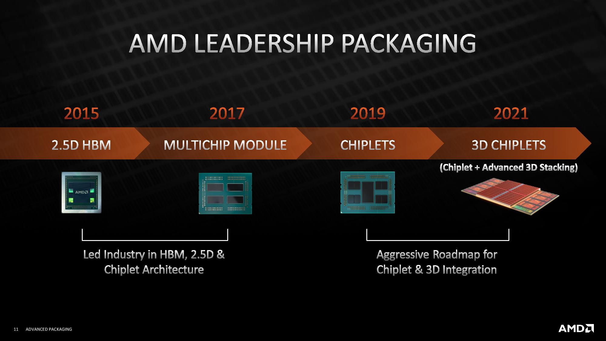
AMD's 3D V-Cache marks the company's first foray into 3D packaging, and the company shared more details behind its manufacturing process during its presentation at Hot Chips 33. As a quick refresher, 3D V-Cache uses a novel new hybrid bonding technique that fuses an additional 64MB of 7nm SRAM cache stacked vertically atop the Ryzen compute chiplets to triple the amount of L3 cache per Ryzen chip.
This new tech can yield up to an amazing 192MB of L3 cache per chip, and AMD has demoed a Ryzen 9 5900X gaining 15% more performance in 1080p gaming with the new cache, which is roughly the amount of performance we could expect from a new CPU microarchitecture and/or process node. However, AMD accomplished this feat with the same 7nm node and Zen 3 architecture that already ships with its standard Ryzen 5000 models. This advance also comes with a single die stacked atop the chip — AMD says it can stack more than one layer in the future, which would boost capacity even further.
AMD divulged after the presentation that it can accomplish similar yields with the new 3D V-Cache chips as it does with standard Ryzen models, meaning it has already jumped the hurdles required to bring the chips, which enter production at the end of the year, to market.
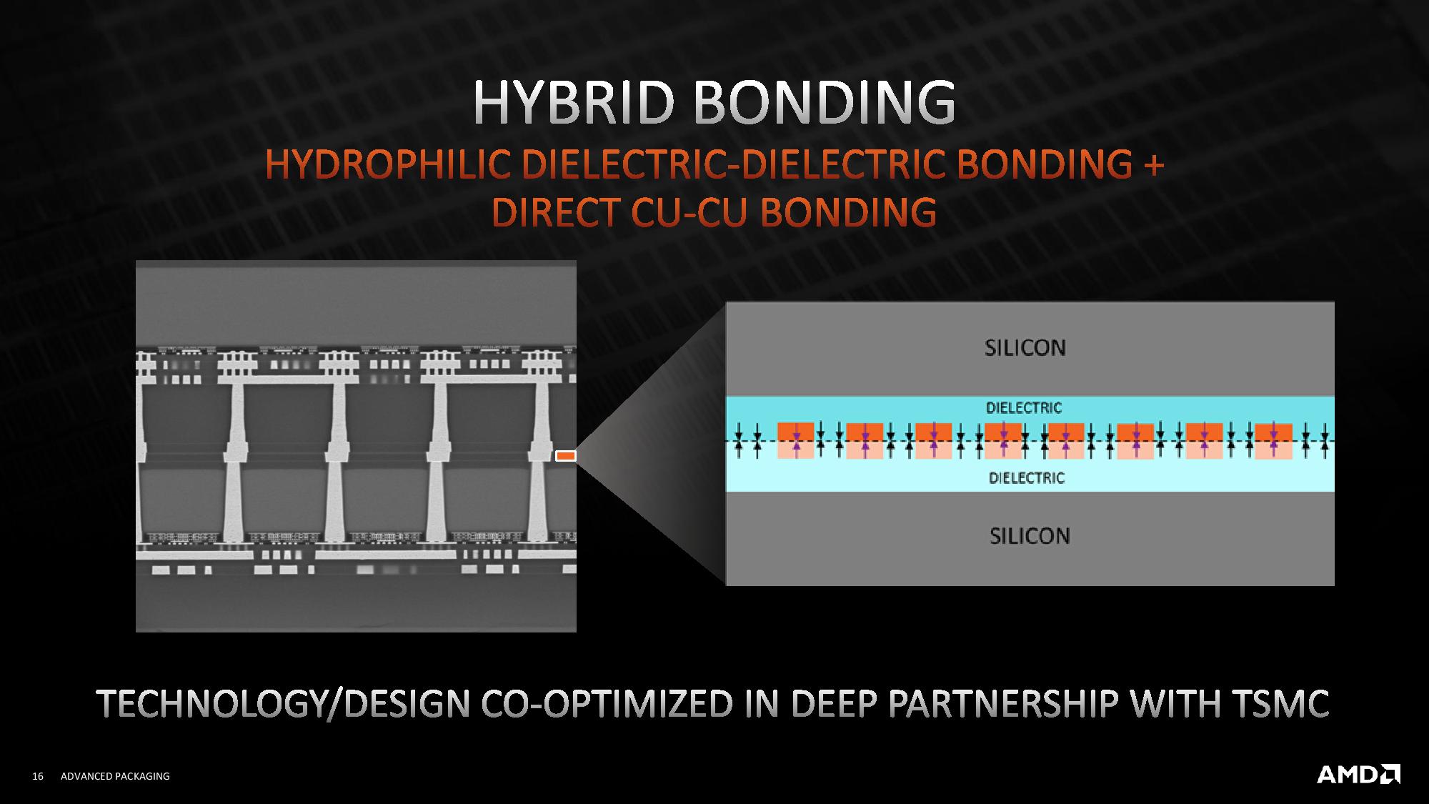
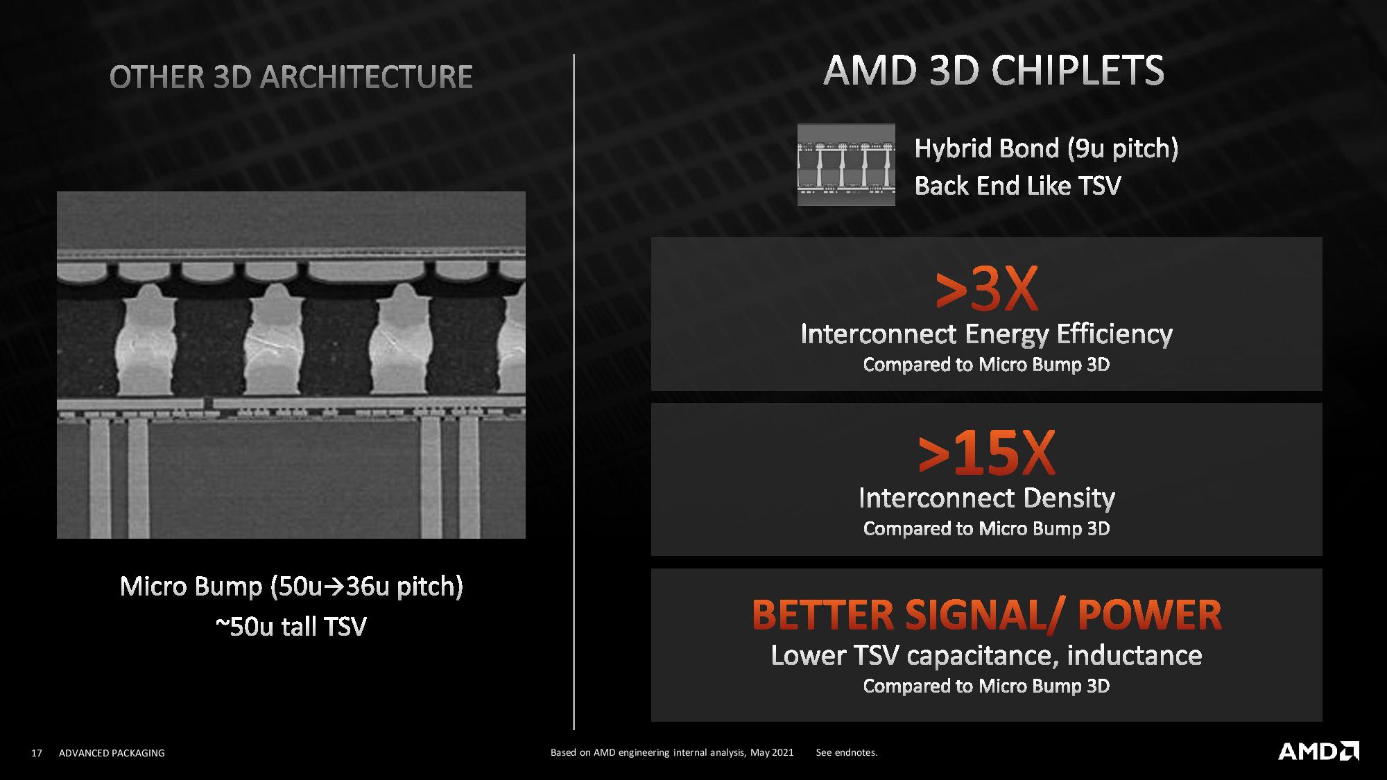
AMD uses TSMC's SoIC process to fuse the SRAM chiplet atop the compute die with direct copper-to-copper dielectric bonding of the TSVs that connect the two die. This technique doesn't use solder microbumps to connect the two chips, resulting in a denser and more efficient interconnect with 200X the interconnect density of 2D chiplets.
TSMC fuses the two chips together with a two-phase bonding technique. The first phase uses a hydrophilic dielectric-to-dielectric bonding process at room temperature, then annealing bonds the dielectric connections. The second phase is a direct copper-to-copper bonding that forms the bonds by solid-state diffusion. AMD says the technique uses silicon fab-like manufacturing with back-end like TSVs, which means the production flow is similar to that of a regular chip.
AMD keeps the SRAM chip centered over the L3 cache on the bottom layer to reduce the SRAM's exposure to heat from the CPU cores. In addition, AMD places structural silicon over the CPU cores using the same hybrid bonding process, thus creating a uniform height for the chiplet that aids with cooling the chip.
Relative to microbump 3D connections, AMD says 3D V-Cache has three times the interconnect efficiency by consuming less than one-third the energy-per-bit, 15X the interconnect density, and better signaling and power delivery characteristics.
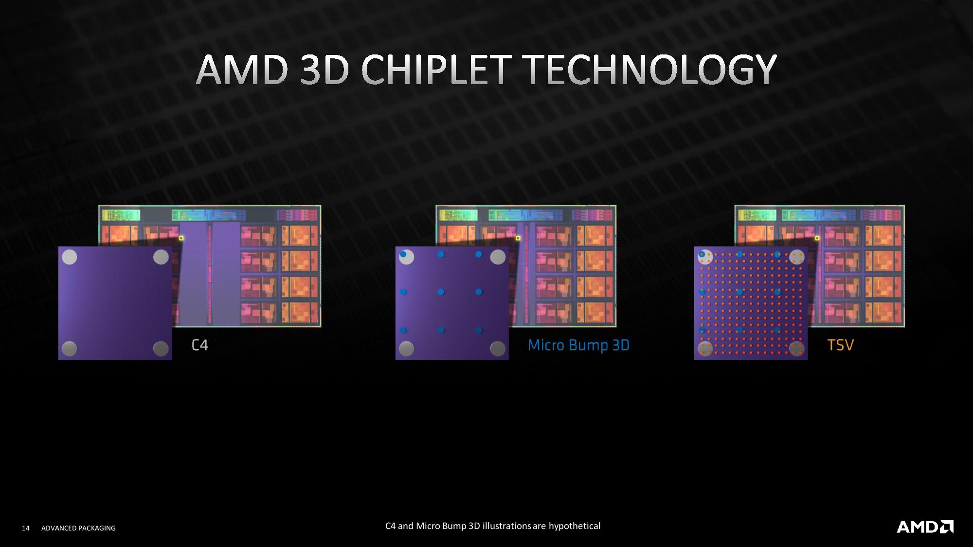
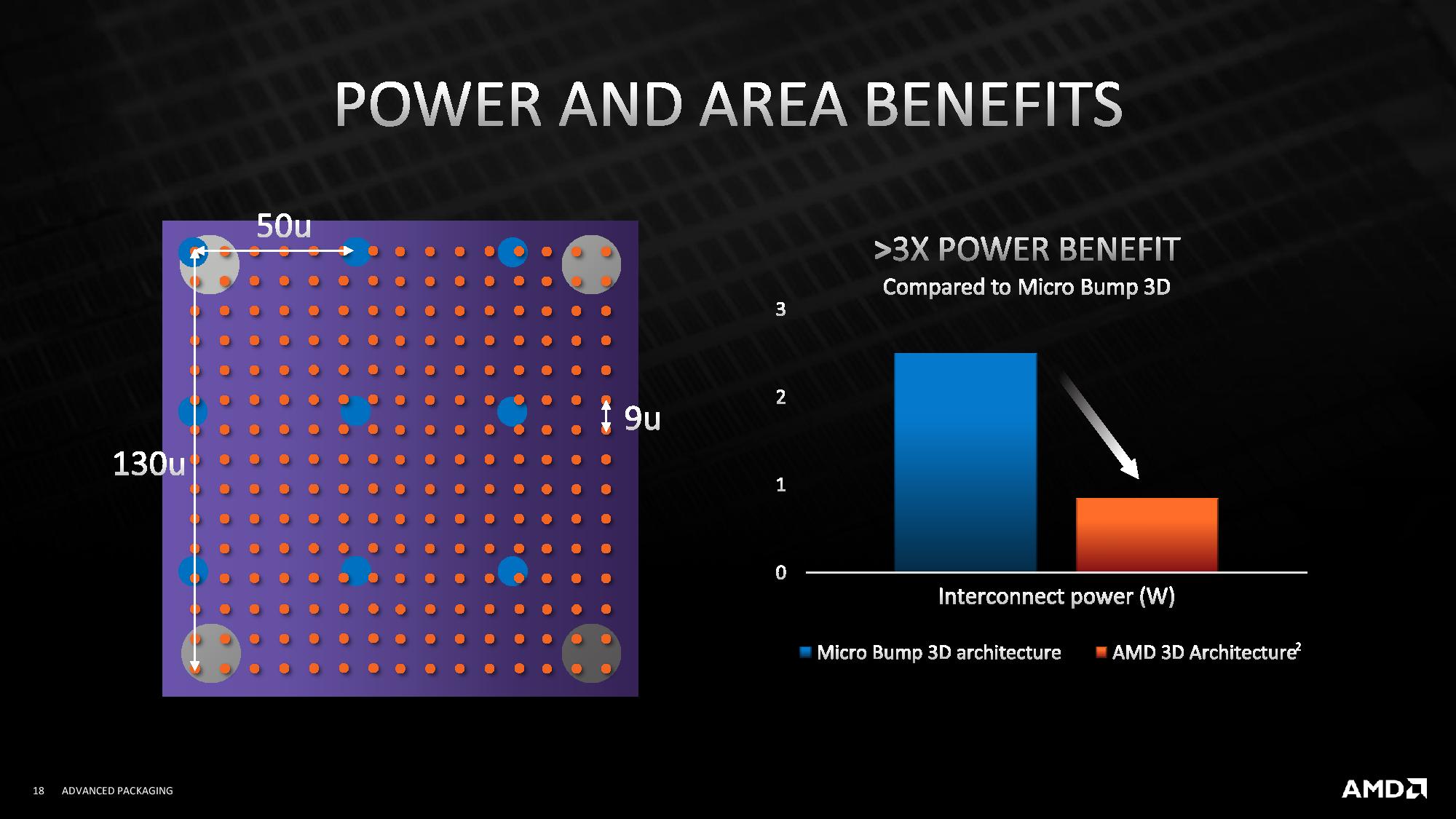
AMD's approach provides 2 TB/s of throughput between the two dies. The company says the latency impact is minimal and within the standard range of a higher-capacity L3 cache (raw access time for cache scales with capacity).
Get Tom's Hardware's best news and in-depth reviews, straight to your inbox.
The first image shows the interconnect density between three different interconnect approaches. While AMD's new interconnect comes with a 9-micrometer (μm) pitch (distance between TSV), standard C4 packaging has a 130 μm pitch, and Microbump 3D comes with a 50 μm pitch.
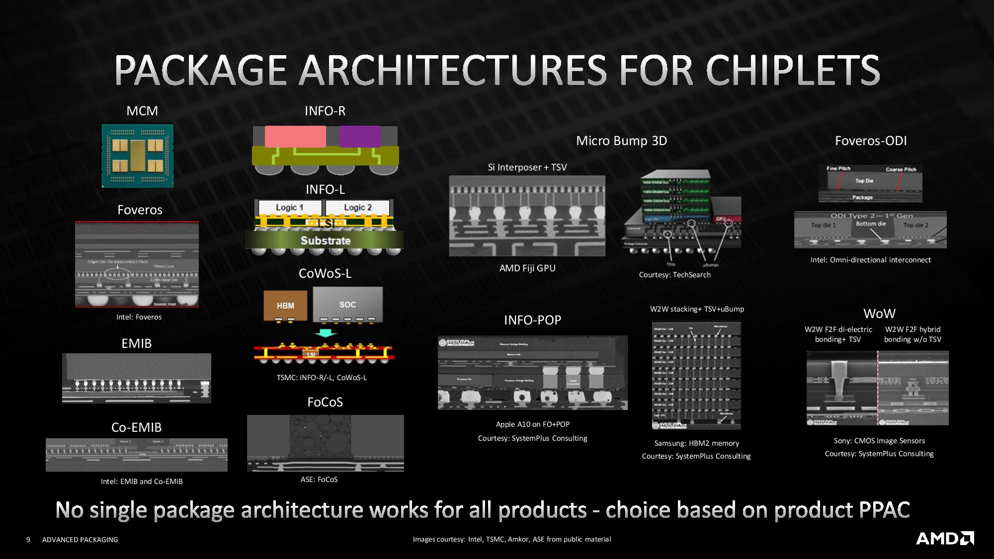
In comparison, Intel's shipping first-gen EMIB connection has either a 55 μm pitch, while its second-gen EMIB that lands in 2023 will have a 45 μm pitch. However, Intel's forthcoming Foveros Direct is the most directly-comparable interconnect tech, and Intel claims it will have a sub-10 μm pitch when it comes to market in late 2023. Meanwhile, TSMC's 9 μm hybrid bonding will come to market sometime early next year in AMD's 3D V-Cache processors.
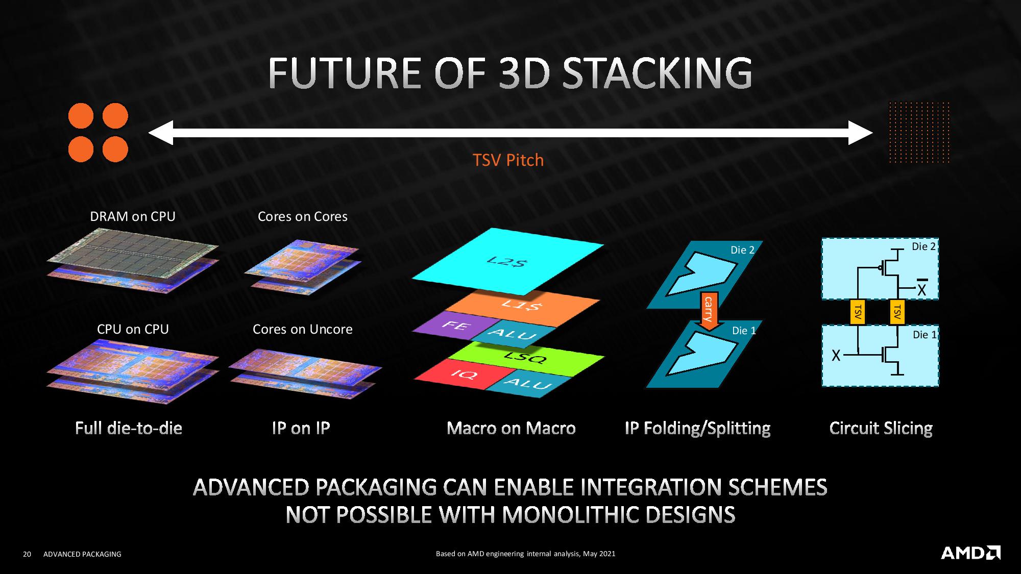
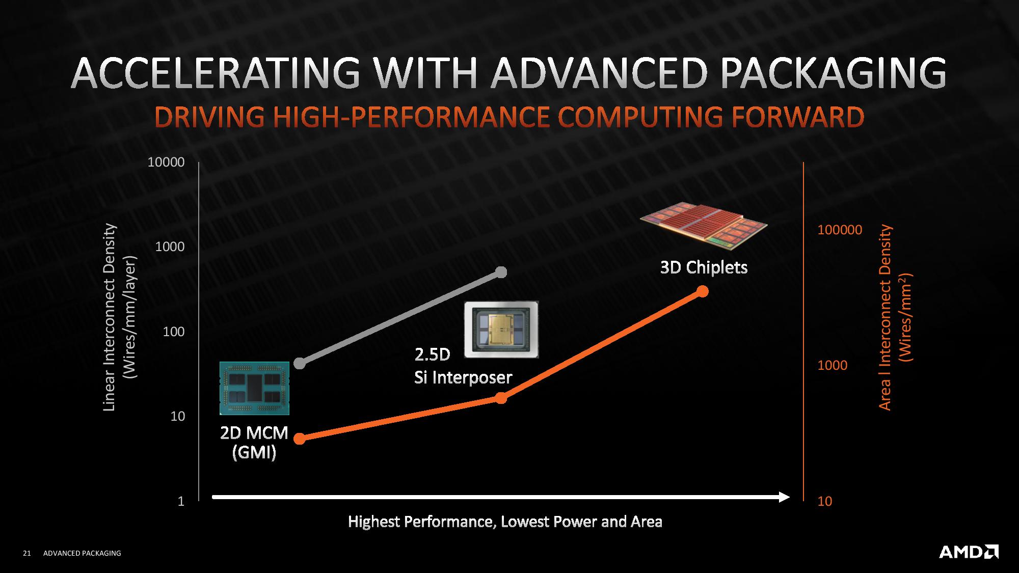
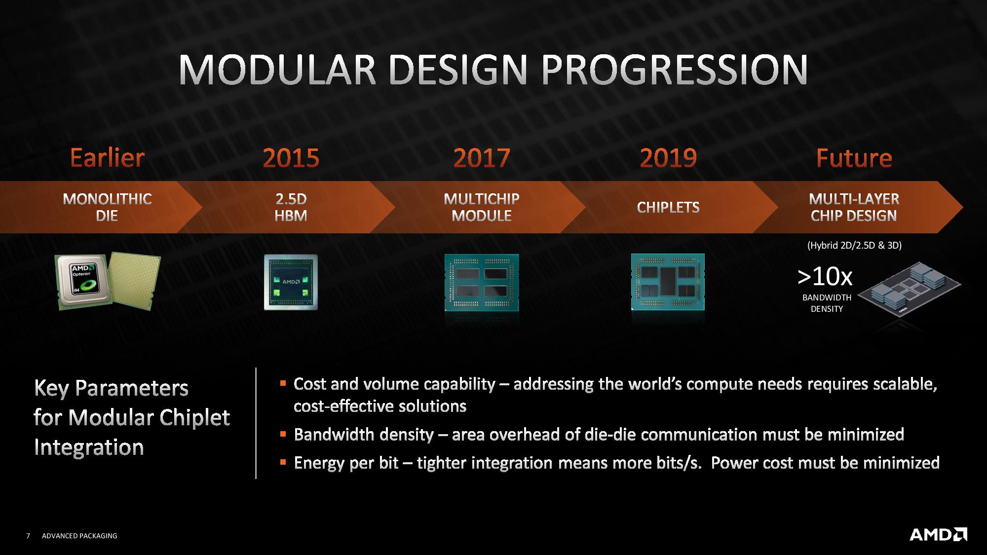
AMD's current memory-on-logic is just the start of a broader trend for the industry. As the TSV pitch improves over successive generations of the technology it will unlock other more refined stacking techniques, like DRAM/HBM on CPU, and stacking entire CPUs on top of CPUs.
Further progression could find even more granular approaches, such as stacking CPU cores on top of other cores, and stacking the cores on top of the uncore (which Intel already does with Lakefield). Even further down the development path, we could see macro-on-macro stacking, which means various elements of the core microarchitecture are stacked atop one another, or even IP folding/splitting and circuit slicing.
Naturally, these are far-off technologies that aren't on the drawing board yet and will provide plenty of challenges, particularly in thermal dissipation, but AMD and other companies do see these techniques emerging in the future.


Paul Alcorn is the Editor-in-Chief for Tom's Hardware US. He also writes news and reviews on CPUs, storage, and enterprise hardware.