Why you can trust Tom's Hardware
3D V-Cache Technology
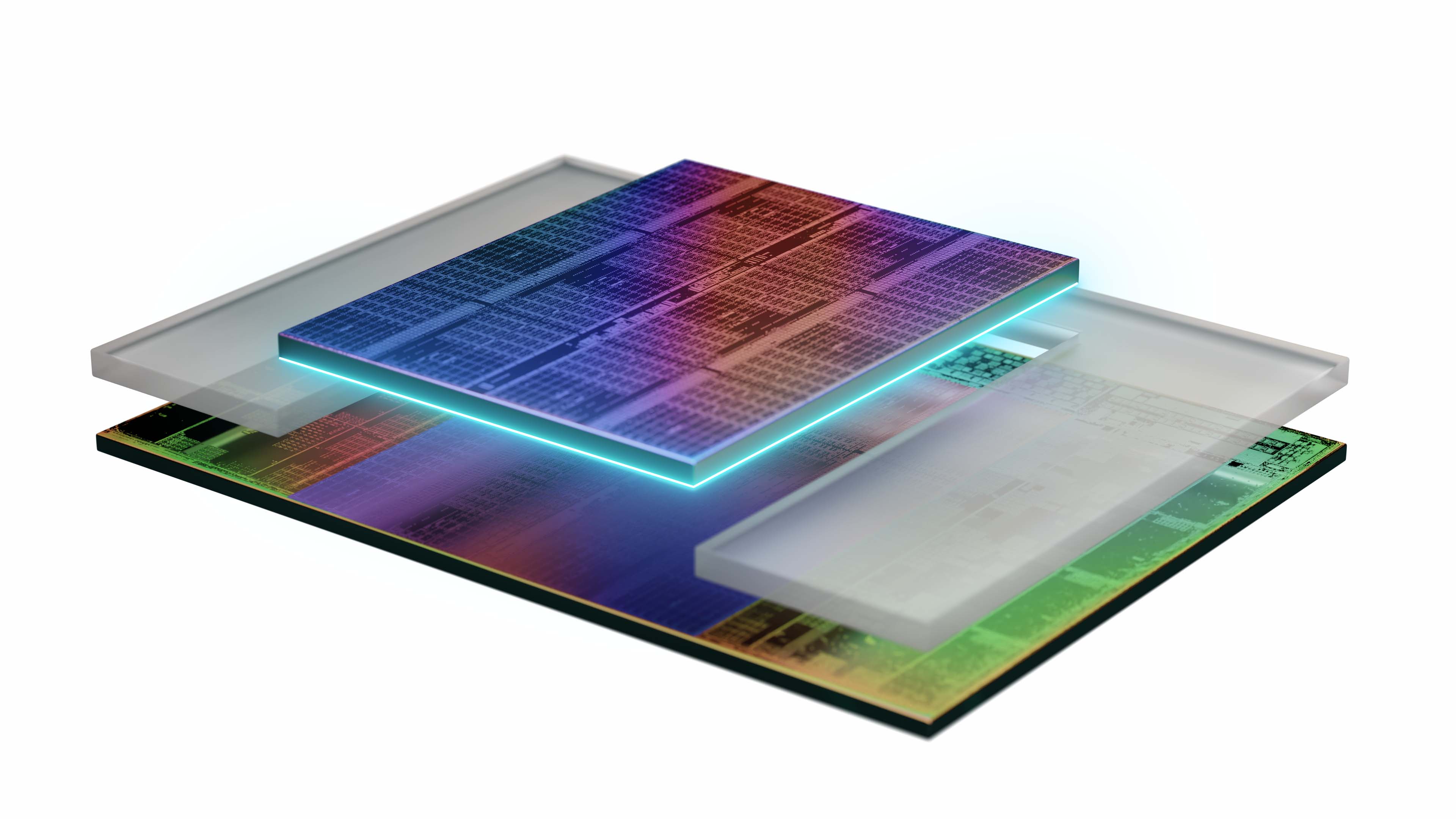
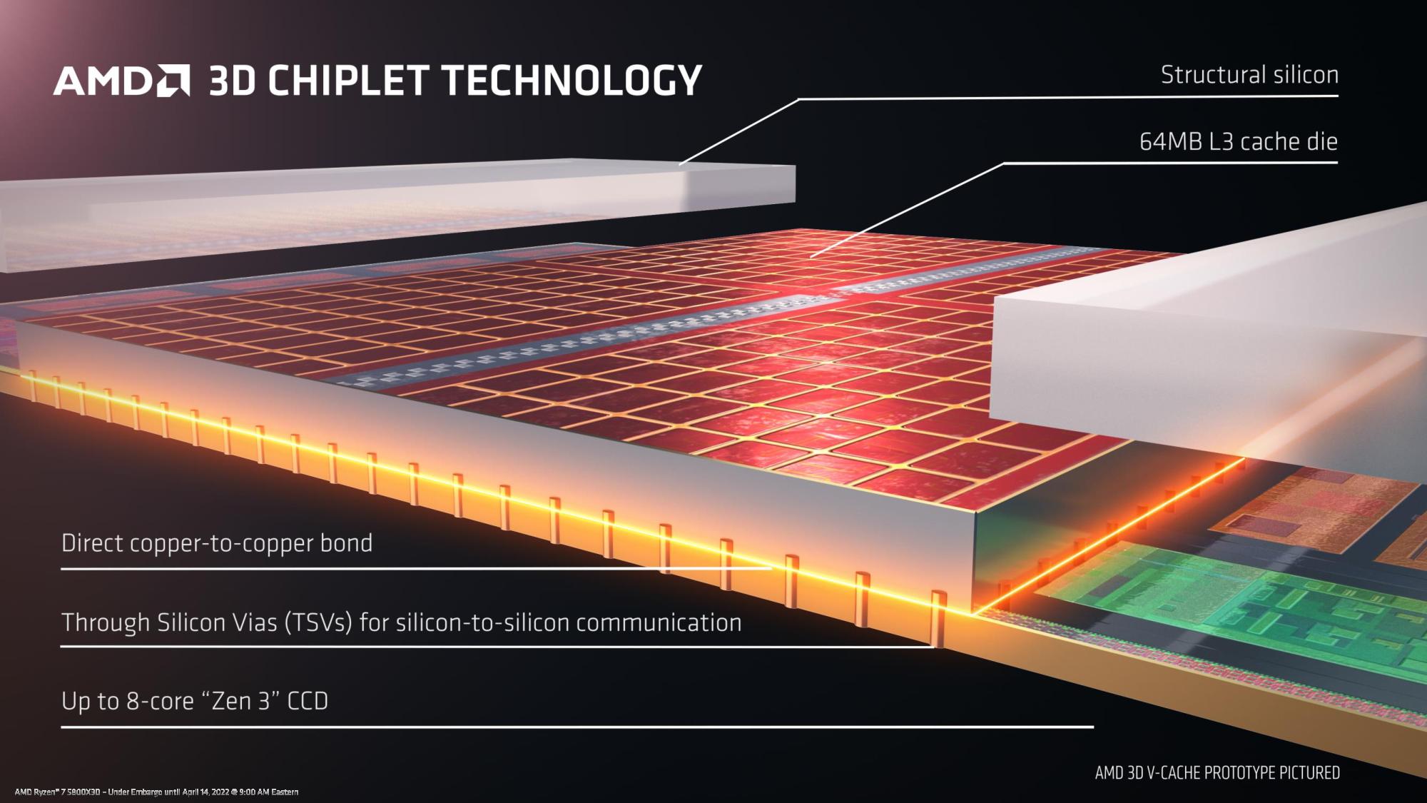
The idea behind 3D V-Cache is relatively simple, but the execution is complex. The basic idea behind any on-chip cache is to keep frequently accessed data as close to the execution cores as possible, thus eliminating high-latency trips to main memory. As a result, the cores don't have to wait for data, thus staying busier and boosting performance. The L3 cache is slower than other caches (like L1 and L2), but its higher capacity means it can store more data, improving the hit rate (the number of times useful data is held in the cache). There's a reason AMD calls it "Game Cache" — L3 cache is very important to performance, and games, in particular, can suffer from high L3 latency or reduced cache capacity/hit rates.
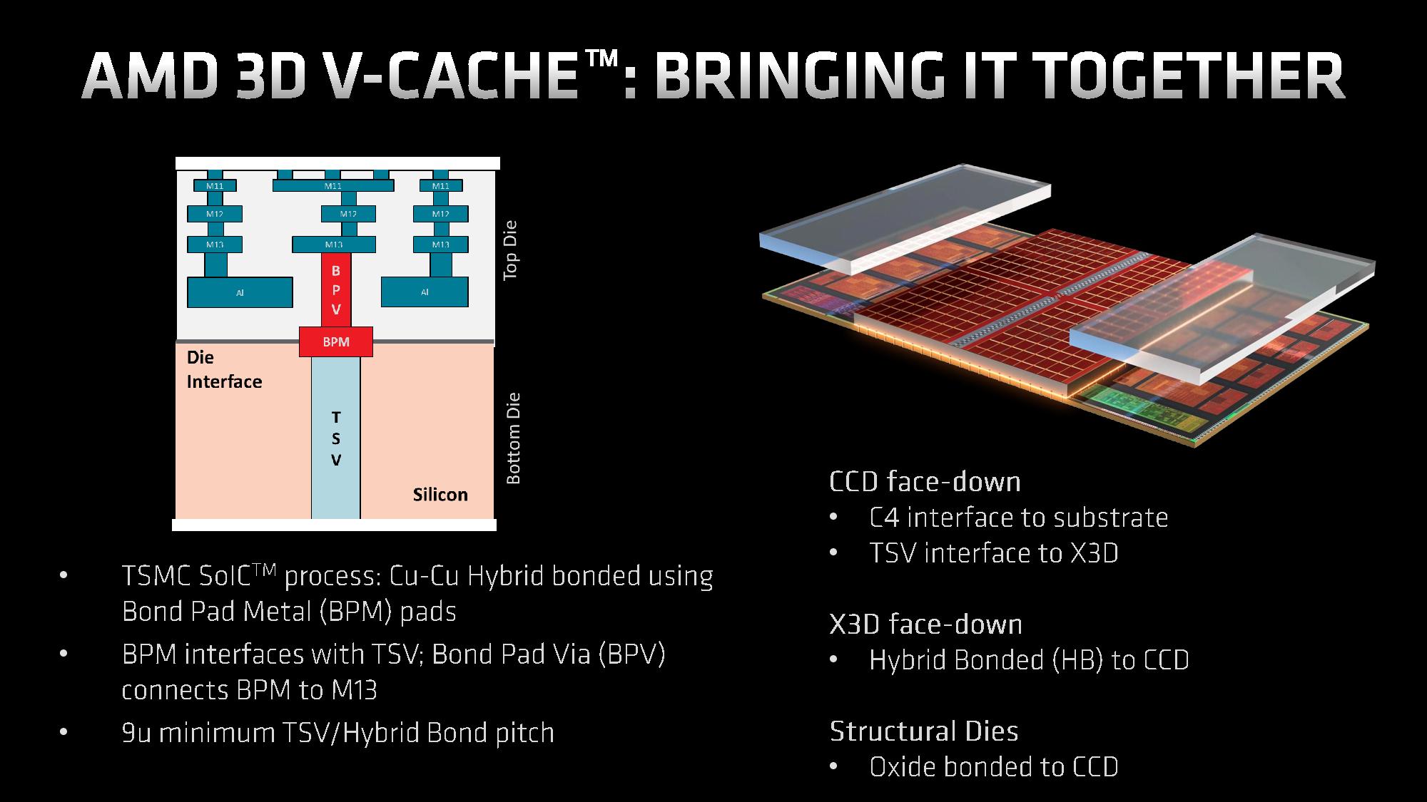
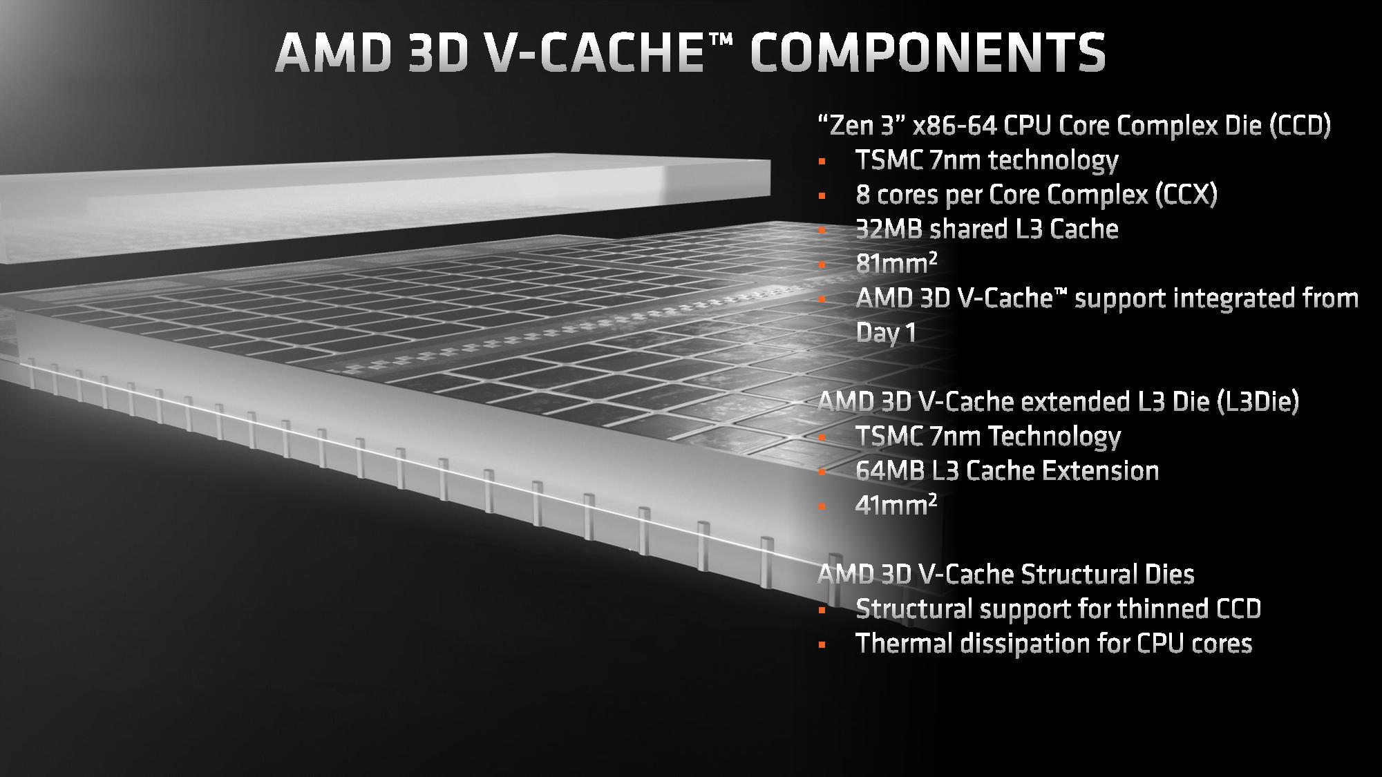
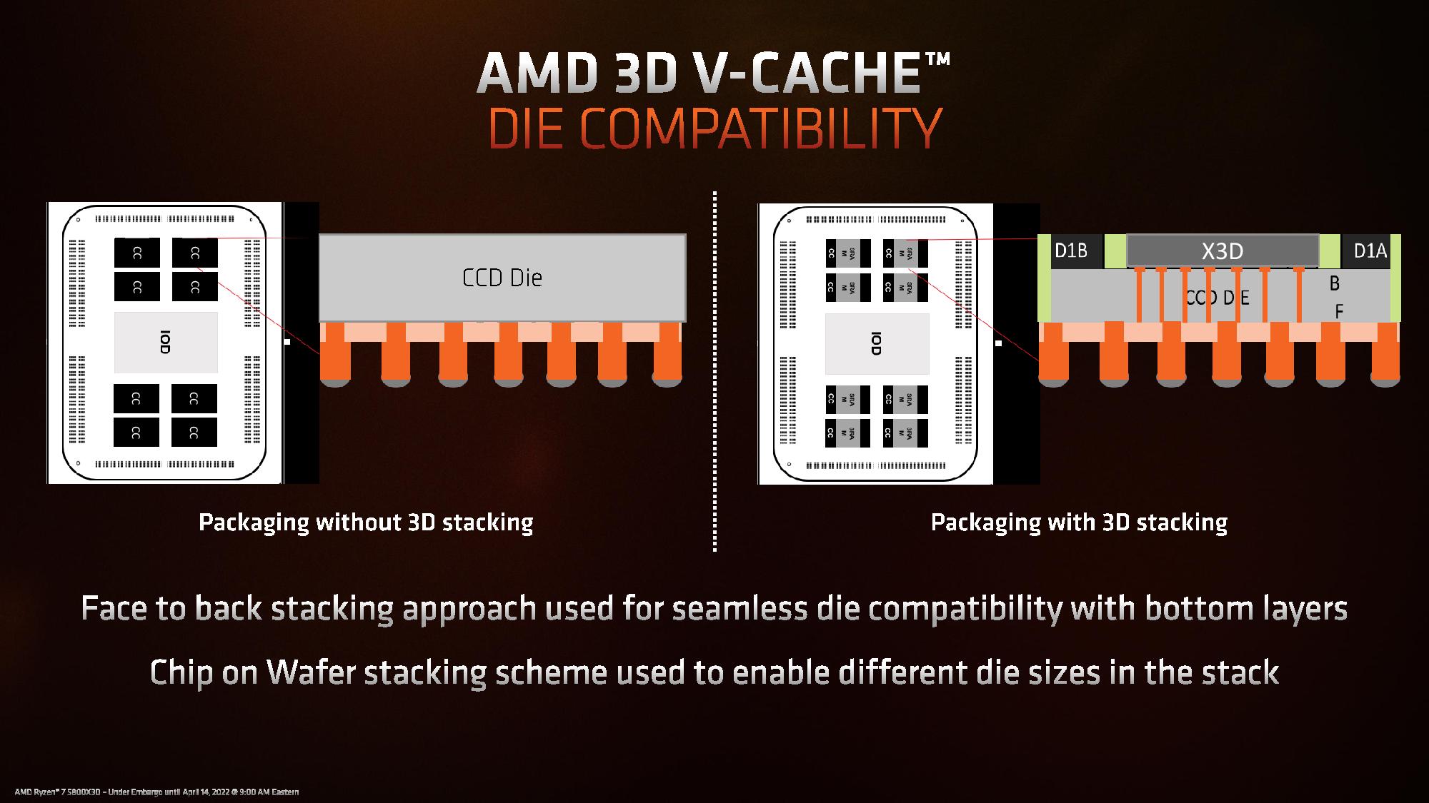
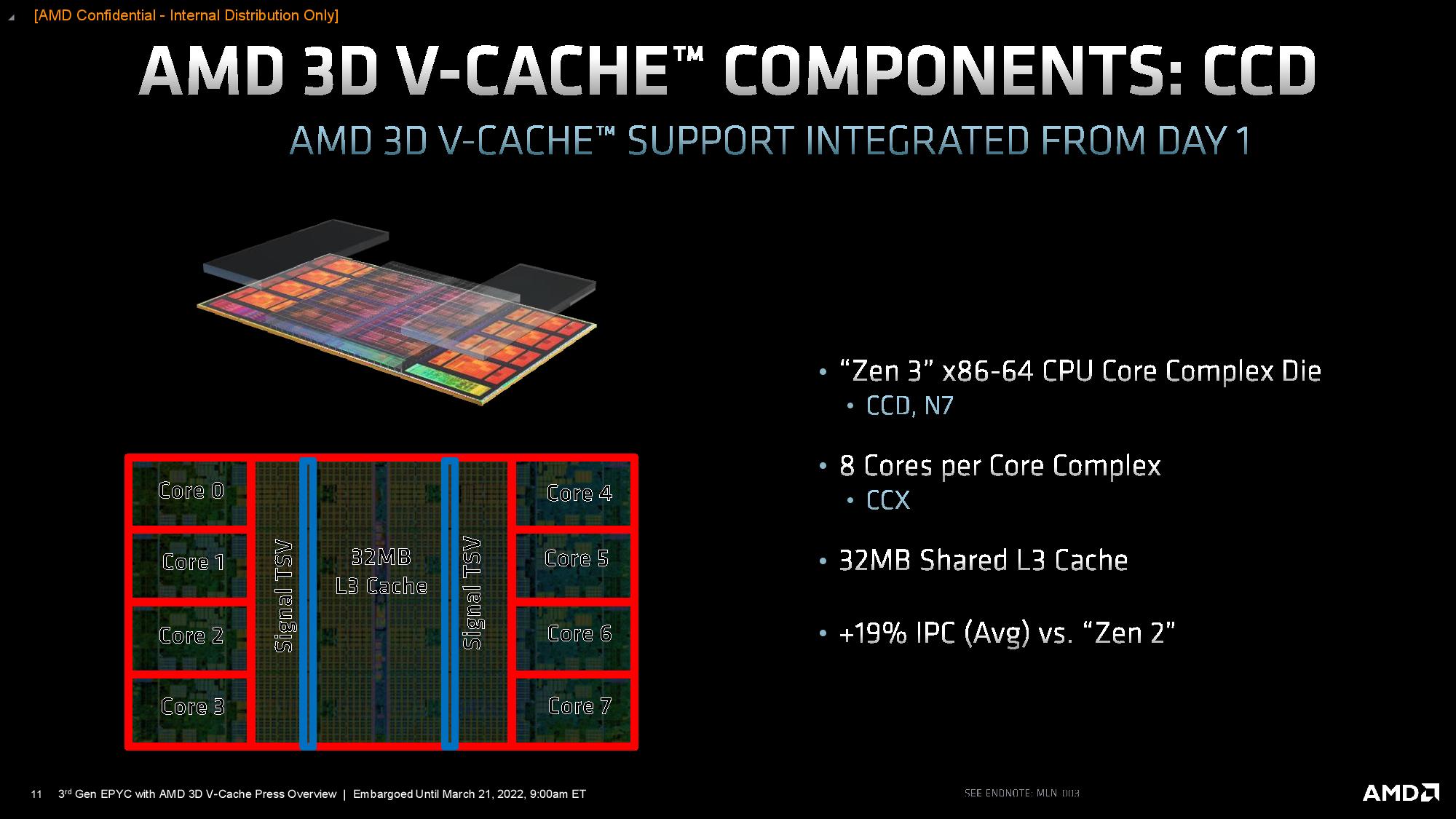
But a big slab of cache is best. As you can see in the above album, AMD stacks an additional SRAM chiplet, connected via TSVs to the lower die, directly in the center of the compute die (CCD) to isolate it from the heat-generating cores on the sides of the chiplet. However, AMD has to use a silicon shim on top of the cores to create an even surface for the heat spreader that sits atop the chiplet. Contrary to popular belief, this is a single shim that wraps around the chiplet on three sides (images in cache testing section). Silicon is an excellent thermal conductor, but the shim and extra SRAM die will inevitably reduce thermal dissipation from the bottom die, thus resulting in less thermal headroom. We show that impact in our boost frequency and thermal load testing. The extra memory also consumes more power.
AMD says overclocking isn't possible because the cache chiplet and the CCD share the same power plane and the effective voltage limit for the SRAM chiplet weighs in at 1.35V. Since the core voltage can't be altered separately, that prevents overclocking the CPU core frequencies. Unfortunately, this also hampers peak chip frequencies during normal operation, so the 3D V-Cache tech does contribute to the 5800X3D’s lower clock speeds. For perspective, the Ryzen 7 5800X has a 1.5V limit, so it can reach higher clock speeds.
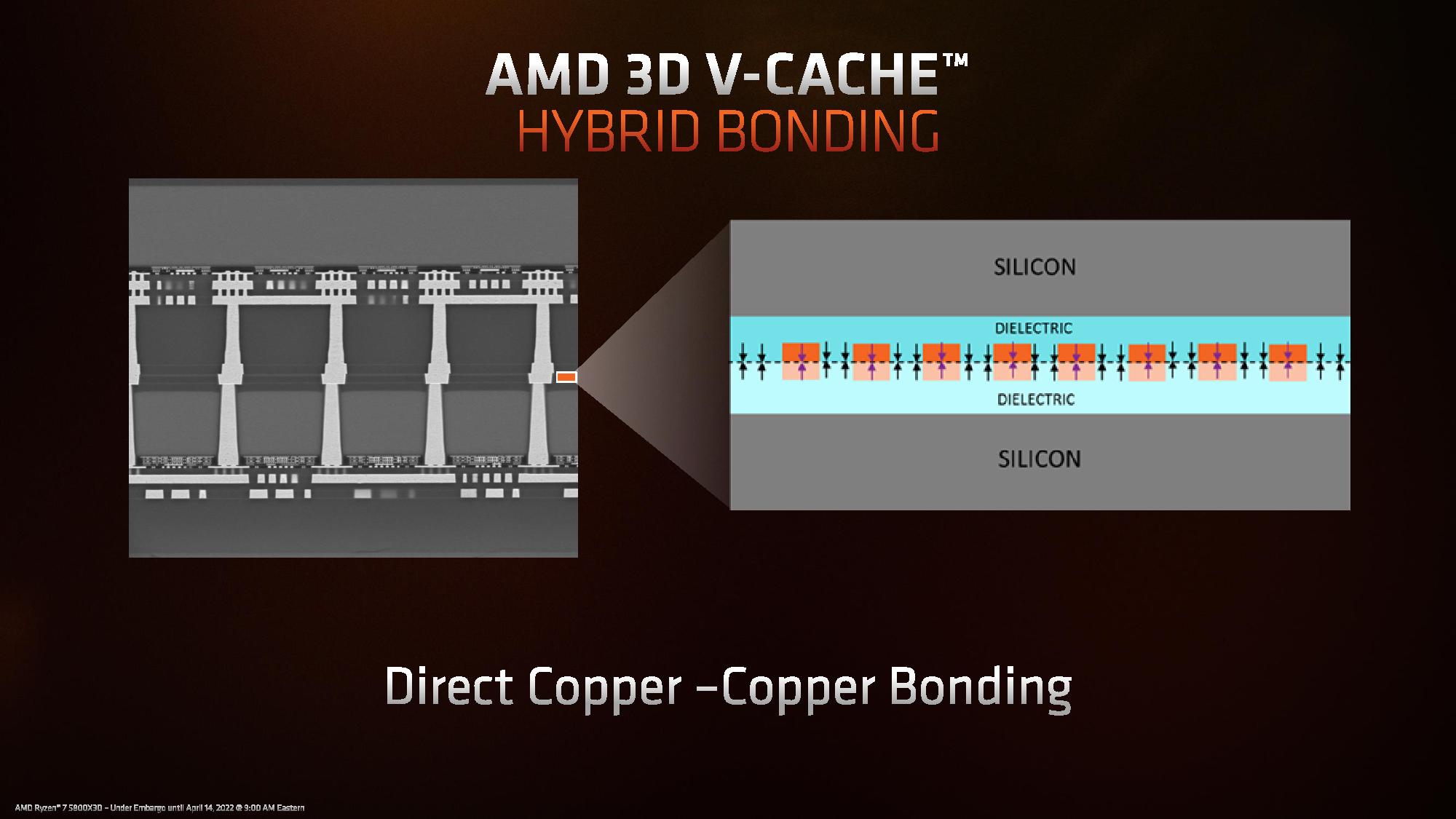
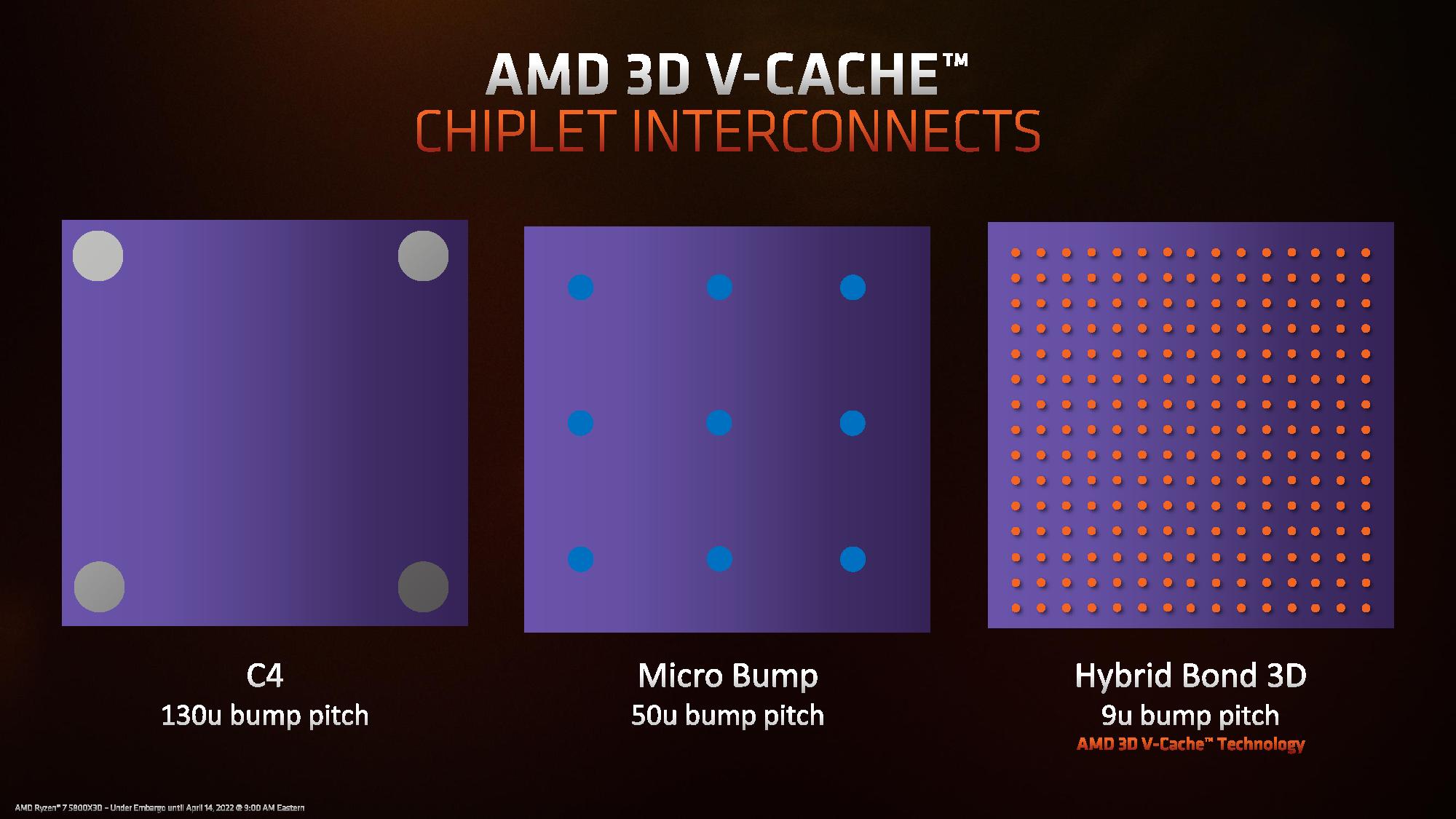
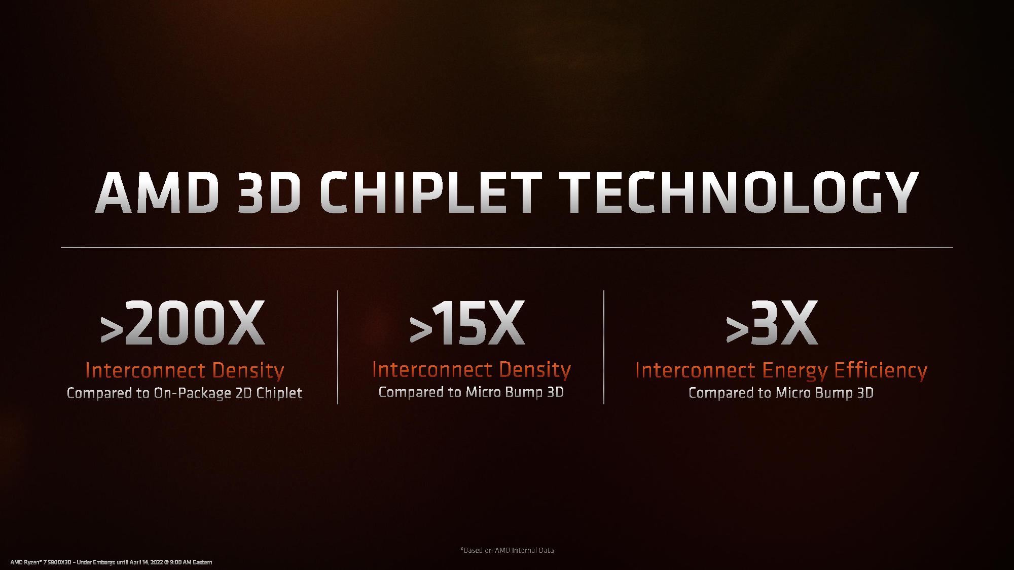
AMD's 3D chip stacking tech is based on TSMC's SoIC technology. TSMC's SoIC is a bumpless chip stacking tech, meaning that it doesn't use microbumps or solder to connect the two die. Instead, the two die are milled to such a perfectly flat surface that the TSV channels can mate without any type of bonding material, reducing the distance between the cache and core by 1000X. That reduces heat and power consumption while boosting bandwidth. You can read much more about the hybrid bonding and manufacturing process here. AMD says the technique uses silicon fab-like manufacturing with back-end like TSVs, which means the production flow is similar to that of a regular chip.
| Row 0 - Cell 0 | 7nm 3D V-Cache Die | 7nm Core Complex Die (CCD) | 12nm I/O Die (IOD) |
| Size | 41mm^2 | 80.7mm^2 | 125mm^2 |
| Transistor Count | 4.7 Billion | 4.15 Billion | 2.09 Billion |
| MTr/mm^2 (Transistor Density) | ~114.6 Million | ~51.4 Million | ~16.7 Million |
As before, the 7nm Core Complex Die (CCD) has 4.15 billion transistors spread out over 80.7mm^2 of silicon. Meanwhile, the new smaller 7nm 3D V-Cache die measures only 41mm^2, yet has 4.7 billion transistors. As you can see in the table, that means it has slightly more than twice the transistor density, which is due to AMD using a density-optimized version of 7nm that's specialized for SRAM. It's also important to remember that a standard compute die includes several types of transistors (libraries, standard cells) for different purposes, so density varies across the die. In contrast, the V-Cache die uses a largely uniform layout.
The L3 cache chiplet spans the same amount of area as the L3 cache on the CCD underneath, but it also has twice the capacity. That's due to the optimized process, but also partially because the additional L3 cache slice is somewhat 'dumb' — all the control circuitry resides on the base die, which helps reduce the inevitable latency overhead associated with fetching data from a separate die (more on that in the cache testing section later).
AMD Ryzen 7 5800X3D 3D V-Cache Design and Latency
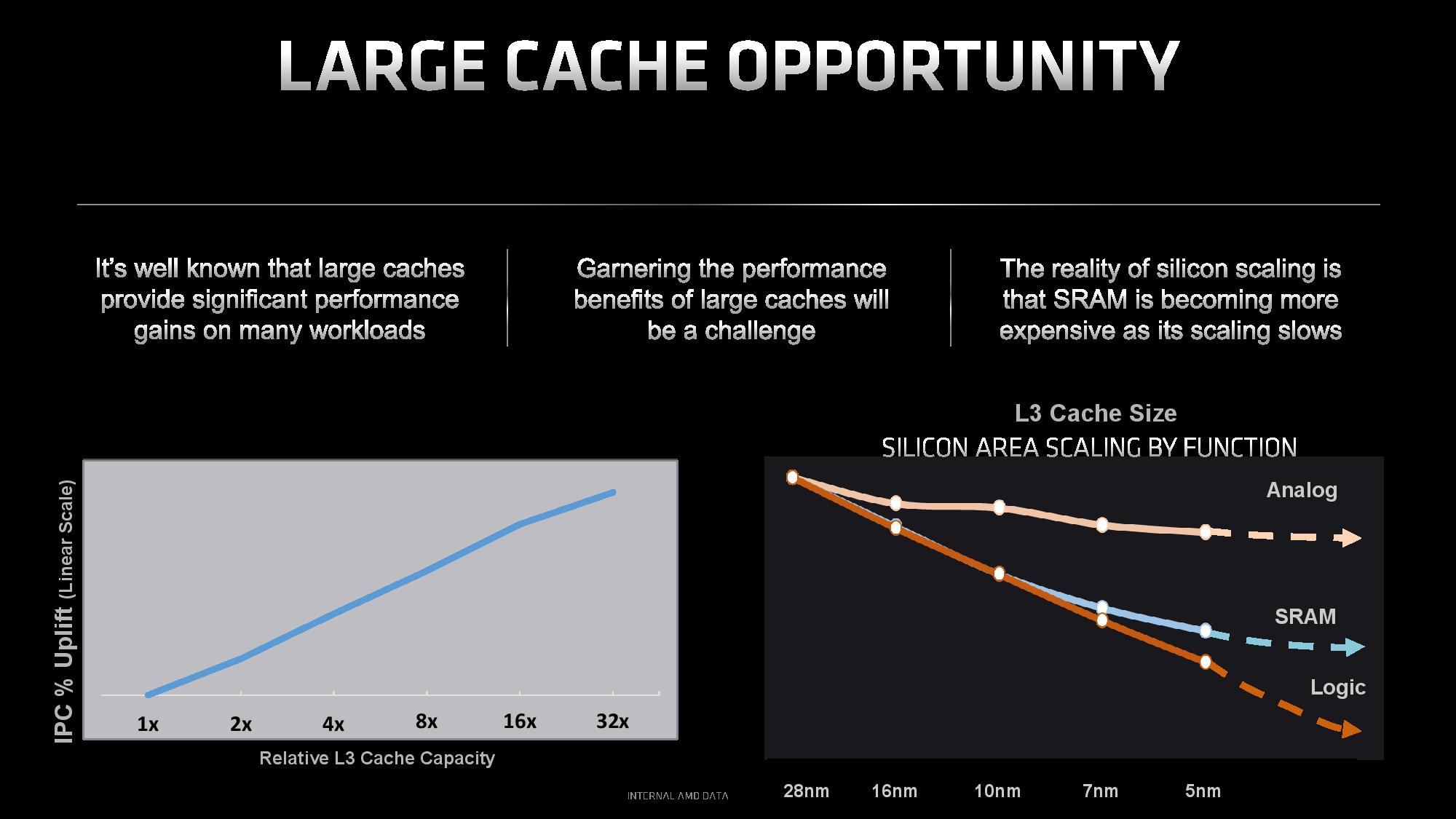
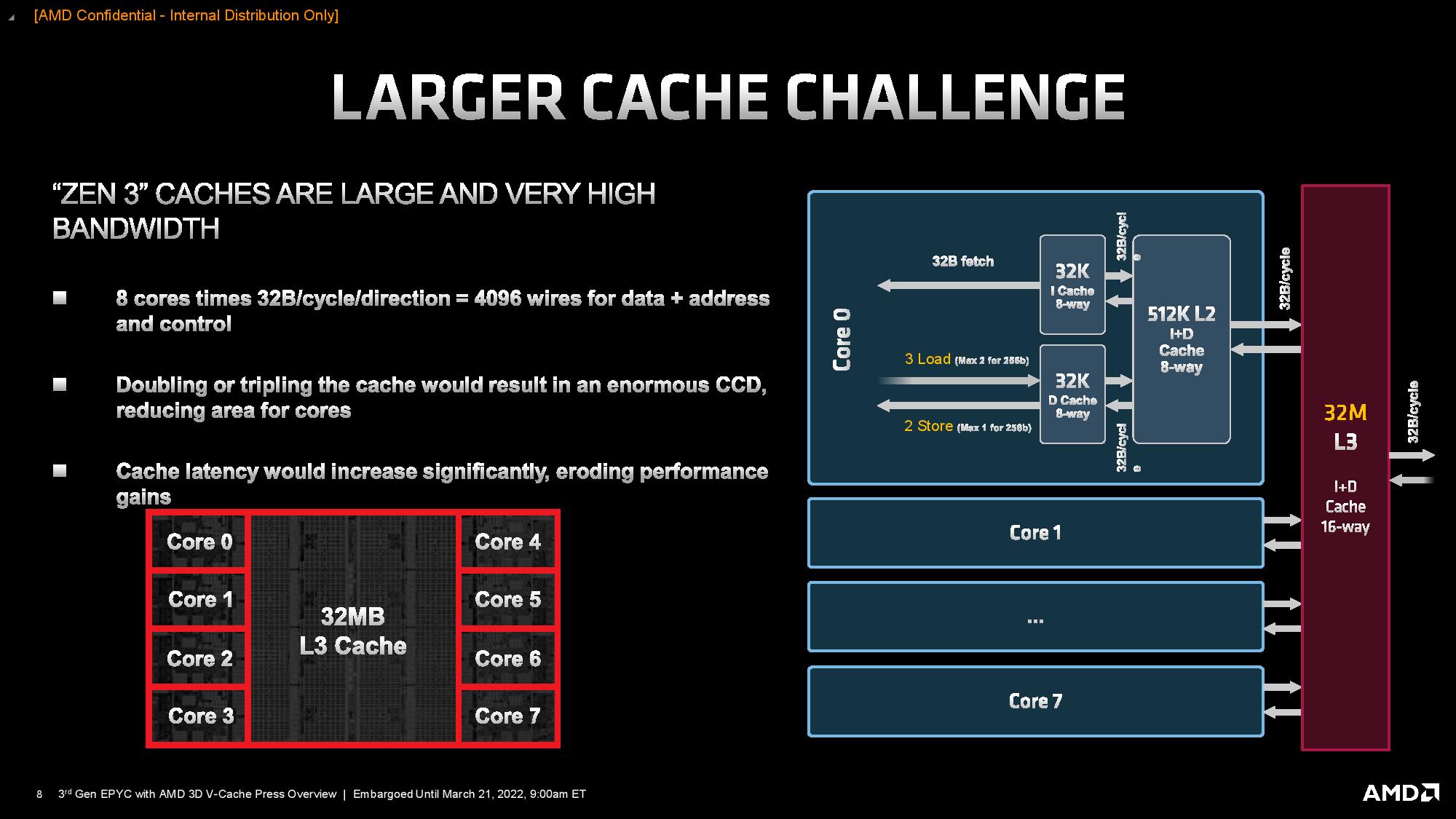
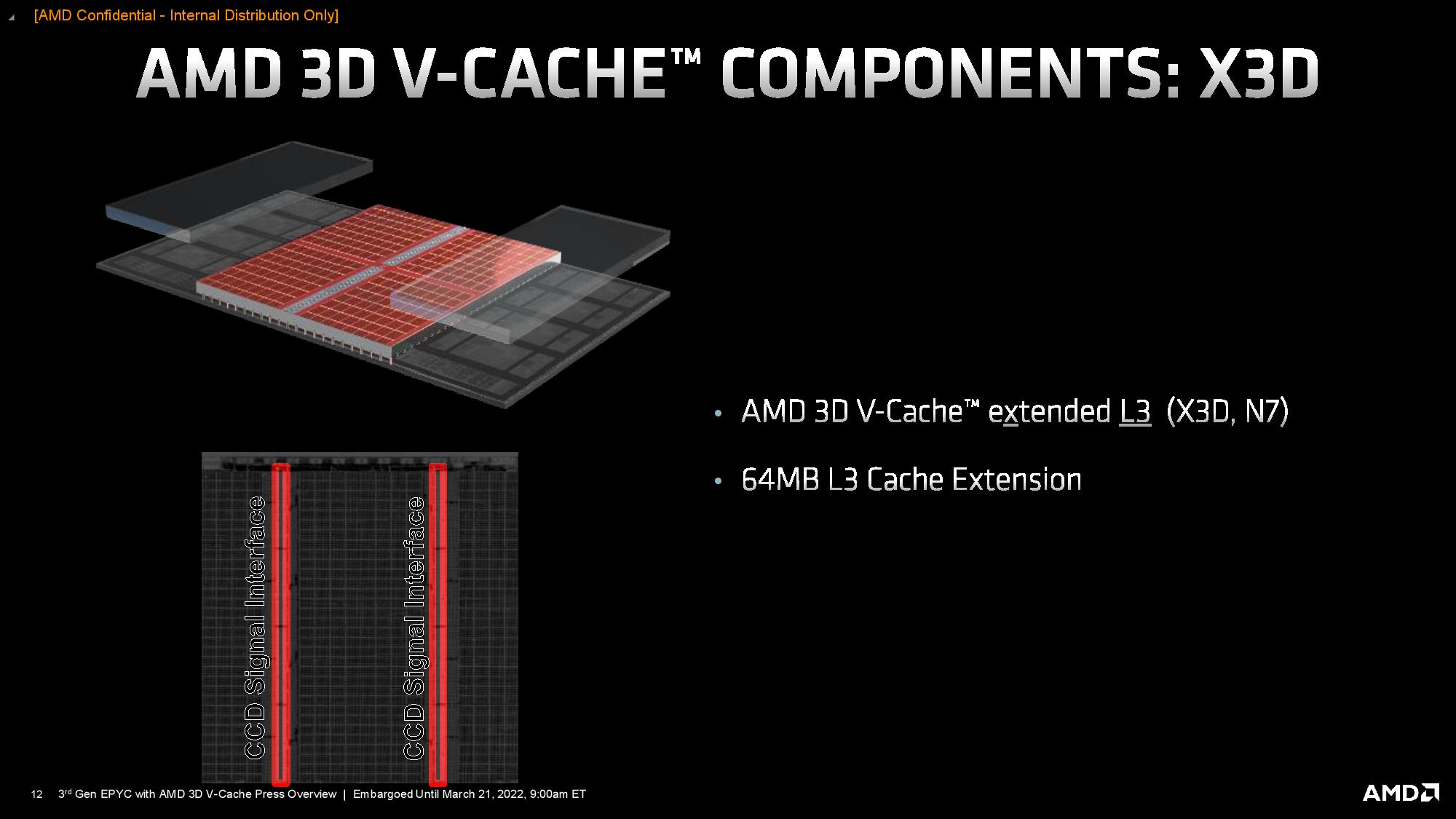

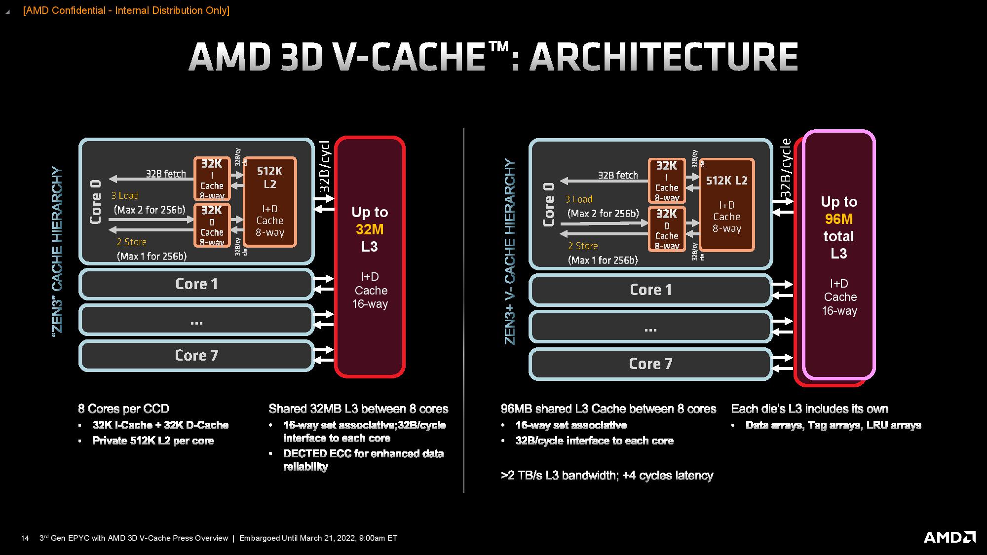
Several factors influenced AMD's decision to use 3D-stacked SRAM, but key among them is that SRAM density isn't scaling as fast as logic density. As a result, caches now comprise a higher percentage of the die area than before, but without delivering meaningful capacity increases. Furthermore, expanding the cache laterally would incur higher latency due to longer wire lengths and eat into the available die area that AMD could use for cores. Additionally, adding another SRAM chiplet in a 2D layout isn't feasible due to the latency and bandwidth impact.
To address those issues, AMD stacks the additional SRAM directly on top of the center of the compute die where the existing L3 resides. This L3-on-L3 stacking allows the lower die to deliver power and communicate through two rows of TSV connections that extend upwards into the bottom of the L3 cache chiplet. These connections go vertically into the upper die and fan out, which actually reduces the amount of distance data has to travel, thus reducing the number of cycles needed for traversal compared to a standard planar (2D) cache expansion. As a result, the L3 chiplet provides the same 2 TB/s of peak throughput as the on-die L3 cache, but it only comes with a four-cycle latency penalty.
| Tom's Hardware | Ryzen 7 5800X3D | Ryzen 7 5800X |
| AIDA - L3 Latency | 13.84 ns | 11.49 ns |
| AIDA - L3 Cycles | 47 clk | 43 clk |
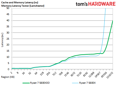
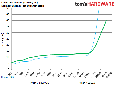
The album above outlines our cache and memory latency benchmarks with the AMD Ryzen 7 5800X3D and the 5800X using the Memory Latency tool from the Chips and Cheese team. These tests measure cache latency with varying sizes of data chunks, and the first slide zooms in on the L3 portion of the cache. Here we can see that the tool measures the Ryzen 7 5800X3D's L3 latency at 12-13ns, whereas the 5800X measures at 10-11ns (the second slide shows the zoomed-out version). We also used AIDA to record the latency measurements, which we listed in the table. Overall, the 3D V-Cache triples the amount of L3 cache but incurs a fairly negligible ~2ns latency impact and a four-cycle penalty.
As mentioned before, the L3 cache chiplet spans the same amount of area as the L3 cache on the CCD underneath, but it has twice the capacity. That's partially because the additional L3 cache slice is somewhat 'dumb' — all the control circuitry resides on the base die, which helps reduce the latency overhead. AMD also uses a density-optimized version of 7nm that's specialized for SRAM. The L3 chiplet is also thinner than the base die (13 metal layers).
AMD produces all of its Zen 3 silicon with TSVs, so all of its Zen 3 silicon supports a 3D V-Cache configuration. However, the TSVs aren't exposed unless they're needed. For 3D V-Cache models, AMD slightly thins the base die as well to both expose the TSV connections and also to maintain the same overall package thickness (Z-Height) as the existing models.
The lack of control circuitry in the L3 chiplet also maximizes capacity and allows AMD to selectively 'light up' only the portions of the cache that are being accessed, thus reducing (and even removing) the power overhead of tripling the L3 cache capacity. In addition, because the larger cache reduces trips to main memory due to higher L3 cache hit rates, the additional capacity relieves bandwidth pressure on main memory, helping to reduce latency and thereby improving application performance from multiple axes. Fewer trips to main memory also reduces overall power consumption.
The L3 cache chiplet consumes significantly less power per square millimeter than the CPU cores. Still, vertical stacking does increase power density, so it's best to isolate it from the heat-generating cores on the sides of the chiplet. However, this would leave a protruding die on top of the CCD, so AMD uses a single silicon shim that wraps around three sides of the L3 chiplet to create an even surface for the heat spreader that sits atop the chiplet. Silicon is an excellent thermal conductor, and the intention is for the shim to allow heat to transfer from the cores up to the heat spreader.
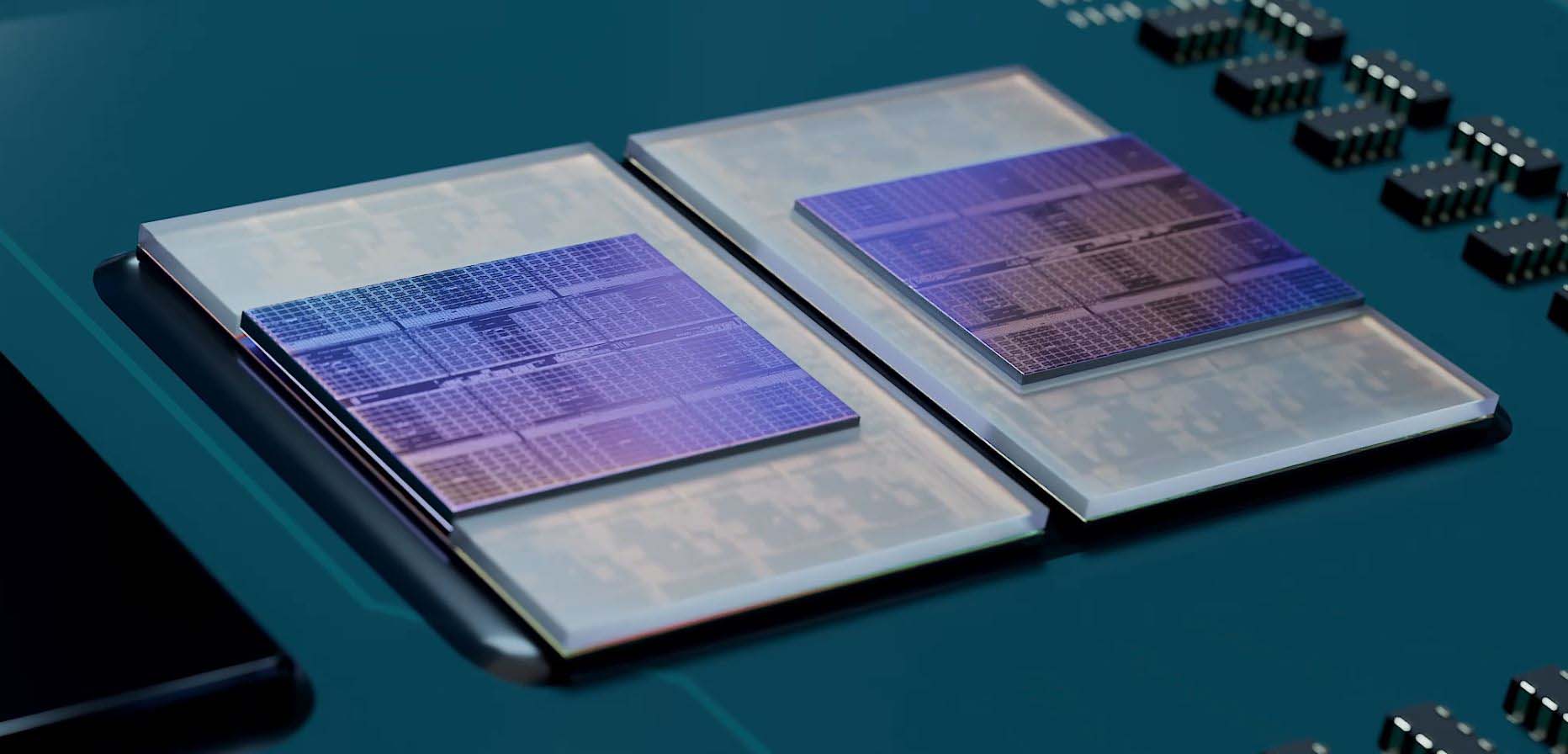
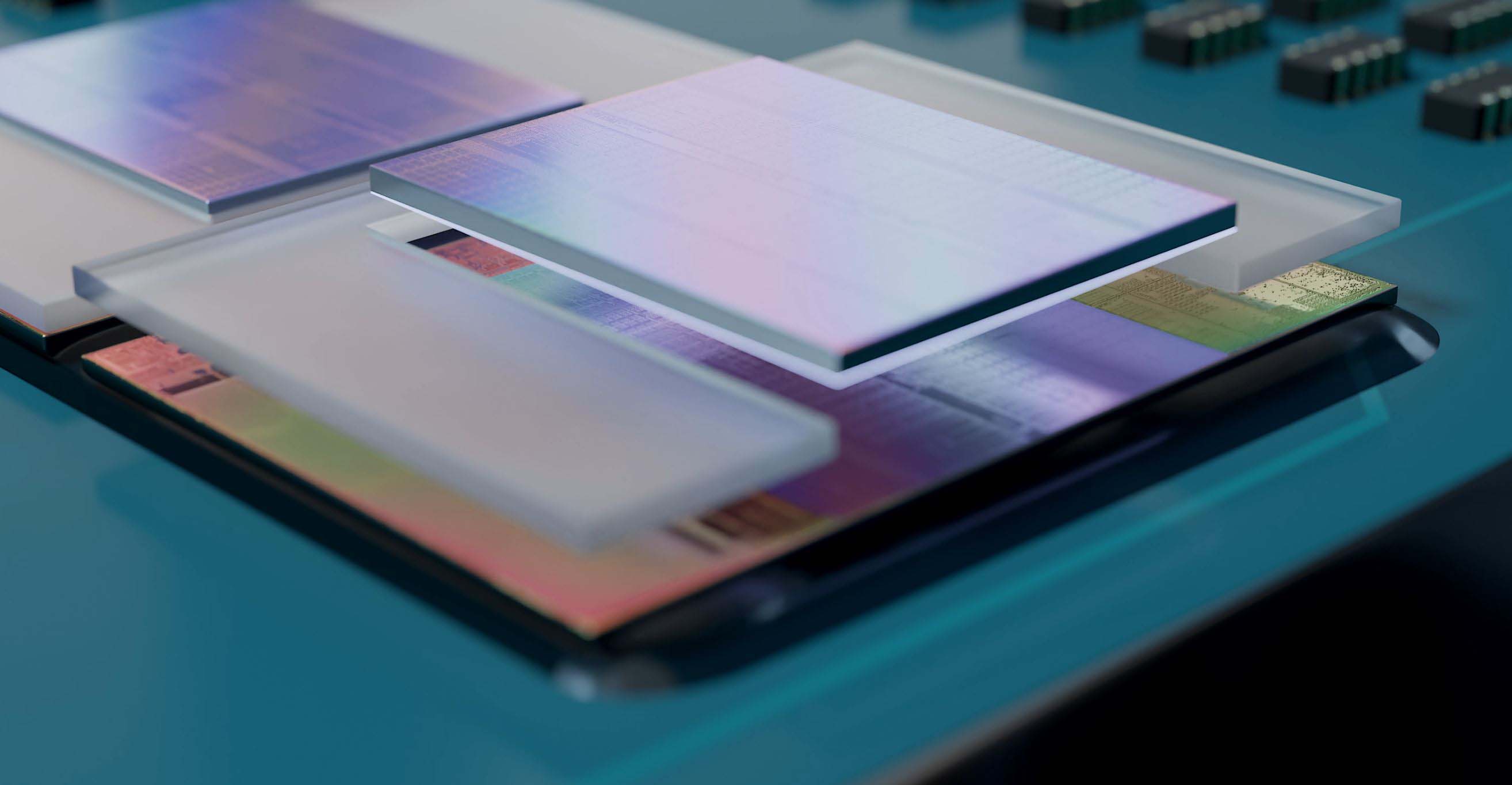

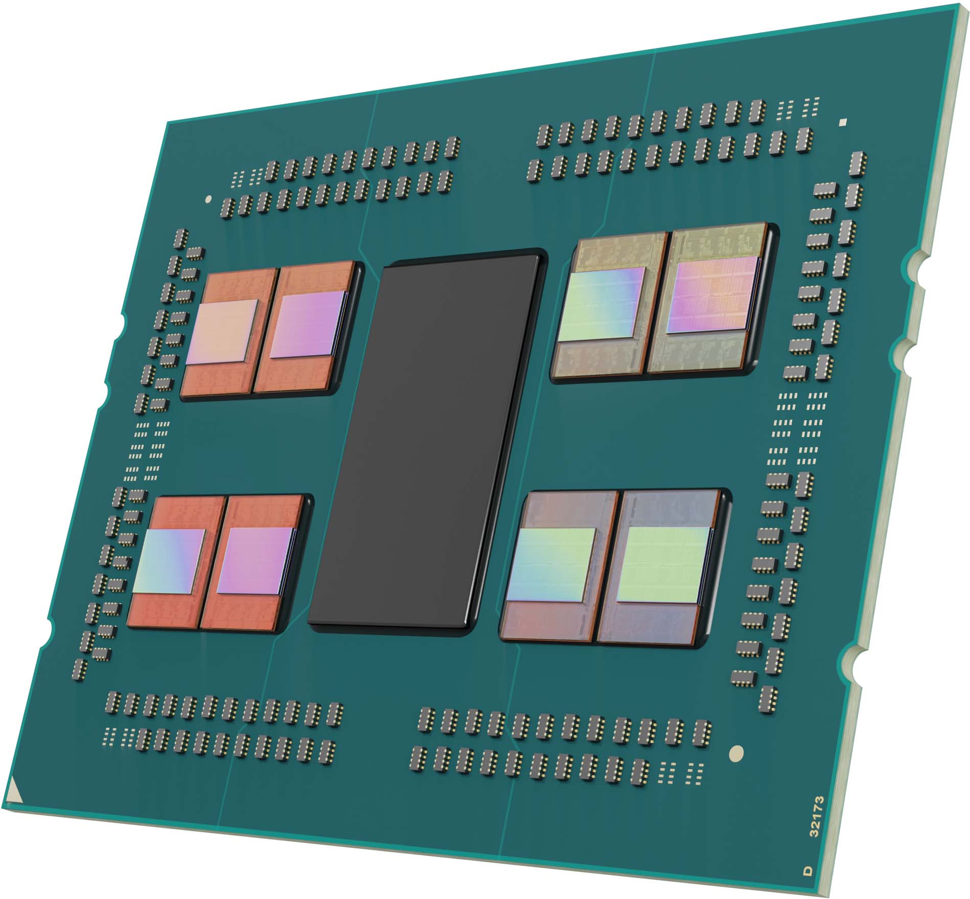
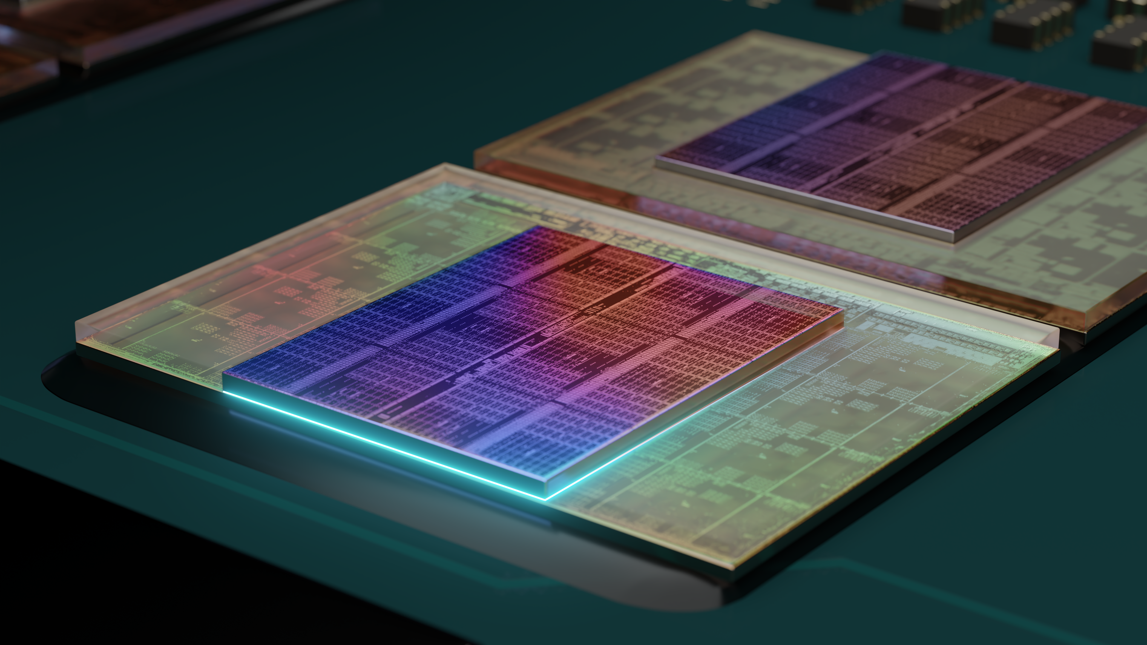
Previous renderings of the design have shown two distinct silicon shims and appeared to show the L3 cache die spanning from one side of the die to the other. However, AMD's materials for the Milan-X launch clearly show one long shim that covers the compute die and a thin portion on the edge of the die that isn't covered by the L3 cache chiplet. This thin expanse of the bottom die includes I/O functions that the chiplet uses to communicate with the I/O die. AMD confirmed that this is the actual layout on all 3D V-Cache processors, like the Ryzen 7 5800X3D, and not the stylized renders shared that show two separate shims.
- MORE: Best CPUs for Gaming
- MORE: CPU Benchmark Hierarchy
- MORE: AMD vs Intel
- MORE: All CPUs Content
Get Tom's Hardware's best news and in-depth reviews, straight to your inbox.
Current page: Ryzen 7 5800X3D: 3D V-Cache Tech, Design and Latency Testing
Prev Page Bolting On More L3 Cache Next Page AMD Ryzen 7 5800X3D Boost Frequencies and Thermal Throttling Tests
Paul Alcorn is the Editor-in-Chief for Tom's Hardware US. He also writes news and reviews on CPUs, storage, and enterprise hardware.
-
Kamen Rider Blade Depending on what applications you're using, there are potentially HUGE performance gains, even on non common workloads.Reply
Level1Techs & Hardware UnBoxed has shown that the 5800X3D is a good value compared to the 12900KS or 12900K -
Makaveli ReplyTom Sunday said:The 5800X3D on the surface looks good. Not the $449 price tag to be sure as many of us given our ongoing dilemma at the gas pumps leaves little or no cash available for higher-end PC fares. Besides AMD being a latecomer to the party with a practically outdated and niche CPU and especially with an all new CPU and hardware generation sitting virtually on our doorstep! At this point in time I would think that many will ‘hold and fold’ until better economic times are in sight and mind. At the latest local computer show the 5800X3D came up in discussion and it was said: “Looks like a very nice chip, but at this late time it’s not a good investment!”
I see this the other way its a fantastic upgrade for those on AM4 that may still be on Zen+ or Zen 2 and will prolong the life of those systems a few more years. Leaving time for pricing to go down on DDR5 when its time to upgrade. -
M42 Clearly, something is wrong with the 12900ks sample used (or the setup) if it can't be overclocked at all, and especially if it is not faster than an overclocked 12700k.Reply
Also, how could any conclusion be made without including 12900k/ks + DDR5 tests?
For example, from a TechSpot review, 12900k FarCry 6 performance was the following (no overclocking):
157 frames/sec - 12900k DDR4-3200
170 frames/sec - 12900k DDR5-6400
Details can be found in the "Gaming Benchmarks" section here:
https://www.techspot.com/review/2443-intel-core-i9-12900ks/
Even after benchmarking the 12900k/ks with DDR5, the 5800X3D might still be ahead in the geometric mean. But since DDR5 prices are dropping I think most people buying a 12900k/ks may end up using higher-end motherboards with DDR5 to squeeze out every last drop of performance. So, can you add some Alder Lake + DDR5 results, please? (thanks!) -
sizzling Reply
This is me. I just upgraded from a 3700X to a 5800X3D. I’m going to get a couple more years out my B450 Tomahawk Max and 2x16gb DDR4. This is paired with a 3080 and 1440p 240Hz monitor. By the time I need to upgrade cpu DDR5 will hopefully be more mature, cheaper and actually bring beneficial improvements for games.Makaveli said:I see this the other way its a fantastic upgrade for those on AM4 that may still be on Zen+ or Zen 2 and will prolong the life of those systems a few more years. Leaving time for pricing to go down on DDR5 when its time to upgrade.
The only thing that I have noticed is my RAM seem to run hotter on the 5800X3D than the 3700X. It now runs at about 45-49c on stock XMP, previously 40-43. -
Alvar "Miles" Udell While it may be the best in gaming for AMD's current offerings, other reviews, such as Techpowerup's, which use an RTX 3080, show the 5800X3D to lead by only 7.4% on vs the 5900X in gaming at 1920x1080 on average. Assuming you aren't using a ~$1500 3090 but a ~$900 3080, are you really telling us that you should buy the 3080X3D instead of spending, currently, $80 more on the 5950X, for twice the number of cores and a much better all around system?Reply -
sizzling Reply
The 5950X is outperformed by the 5900X for gaming, so if gaming is the main concern then it makes sense to compare to a 5800X or 5900X.Alvar Miles Udell said:While it may be the best in gaming for AMD's current offerings, other reviews, such as Techpowerup's, which use an RTX 3080, show the 5800X3D to lead by only 7.4% on vs the 5900X in gaming at 1920x1080 on average. Assuming you aren't using a ~$1500 3090 but a ~$900 3080, are you really telling us that you should buy the 3080X3D instead of spending, currently, $80 more on the 5950X, for twice the number of cores and a much better all around system? -
Alvar "Miles" Udell Replysizzling said:The 5950X is outperformed by the 5900X for gaming, so if gaming is the main concern then it makes sense to compare to a 5800X or 5900X.
True, but not in applications, which is half of this test, and the 5950X beats the 5900X quite handily due to having more cores. And since they compared it against an Intel processor with 16 cores, the 12900K, as well as the 12900KS variant, then they should have included a 16 core AMD processor as well for good measure, even though the 12900K and KS are quite a bit faster anyway. -
sizzling Reply
True, but this review is about the 5800X3D which is being pushed as a gaming cpu, nothing more. Therefore it’s reasonable to compare on that basis. If you are not after a purely gaming cpu the 5800X3D probably does not make sense.Alvar Miles Udell said:True, but not in applications, which is half of this test, and the 5950X beats the 5900X quite handily due to having more cores. And since they compared it against an Intel processor with 16 cores, the 12900K, as well as the 12900KS variant, then they should have included a 16 core AMD processor as well for good measure, even though the 12900K and KS are quite a bit faster anyway. -
-Fran- The biggest winners with the 5800X3D are AM4 owners; the people that actually trusted AMD and, well, they have fully delivered, I'd say. I personally didn't go with the 5800X3D, because the 5900X dropped to under $400 and that's just way too good as an upgrade (I got it for £370). I've gone through 3 Zen generations (2700X, 3800XT and now the 5900X) and while I still think the 9K gen from Intel is still good, I can't help but feel kind of sorry for them. Almost the same for 10K gen owners, but the 10700K is still a great CPU in my eyes and let's not talk about 11K gen.Reply
Also, this thing is still 8 cores and 16 threads, it's not like it suddenly got degraded to a 4 core 8 threads CPU. I'm sure it should be fairly similar to the 11700K or at least 10700K and those you wouldn't say are slouches, no? Perspective is as common as the common sense, innit?
Regards. -
Alvar "Miles" Udell The biggest losers are people like me who bought a high end X370 motherboard trusting AMD to support all AM4 processors on all AM4 motherboards like they said at the beginning, then bought a X570 motherboard after they said no Zen 3 support on X370 motherboards only for them to then change their minds and actually support Zen 3 on X370 motherboards...Reply
