Why you can trust Tom's Hardware Our expert reviewers spend hours testing and comparing products and services so you can choose the best for you. Find out more about how we test.


The Zen 4 architecture first debuted with the company’s Ryzen 7000 processors, so it is now a well-known quantity. AMD says the Zen 4 architecture is an iterative advance over Zen 3. However, Zen 5, which arrives in 2024, will be a grounds-up redesign.
AMD made several advances, but widening the front end to better feed the execution units and improving branch prediction account for 60% of the IPC gain. AMD also increased the op-cache by 1.5x, moved to a two-branch-per-cycle prediction, improved the load/store units, and doubled the L2 cache capacity. The increased L2 cache capacity results in an additional 2 cycles of L2 latency and adds 4 cycles to L3 latency. AMD says this increased latency isn’t too detrimental because the increased cache capacity provides higher hit rates that largely offset the penalty.
AMD has enabled support for AVX-512 instructions, VNNI, and BFloat 16, among a host of other AVX-512 instructions that match the instruction set supported by Intel’s Ice Lake/Cooper Lake. AMD describes its AVX-512 implementation as a 'double-pumped' execution of 256-bit wide instructions. This means that it actually takes two clock cycles to execute an AVX-512 instruction (256b data path), but the architecture executes the issue and retire for AVX-512 in one operation.
AMD’s approach provides compatibility with AVX-512 and still boosts performance. This approach also saves die area and defrays the frequency and thermal penalties typically associated with Intel's processors when they execute AVX-512 workloads. In other words, clock rates won’t drop dramatically (they can increase in some cases), and temperatures won’t skyrocket when the processor executes these types of workloads.
AMD’s AVX-512 implementation results in lower throughput per clock than Intel's method, but the higher clocks obviously offset at least some of the penalty. AMD says AVX-512 provides a 30% increase in multi-core FP32 workloads over Zen. Genoa also offers increases of 4.2x, 3x, and 3.5X in NLP, image classification, and object detection throughput by leveraging INT8.
AMD says the net effect of its Zen 4 architectural enhancements is a 14% increase in IPC over Zen 3. Our own measurements generally agree with those claims, though it is noteworthy that IPC can vary by workload. AMD specc’d the IPC gain at 13% for the Zen 4 architecture when it released the desktop PC Ryzen models, but has apparently reached a 14% value with the different mix of server workloads it used to quantify IPC uplift for Genoa.
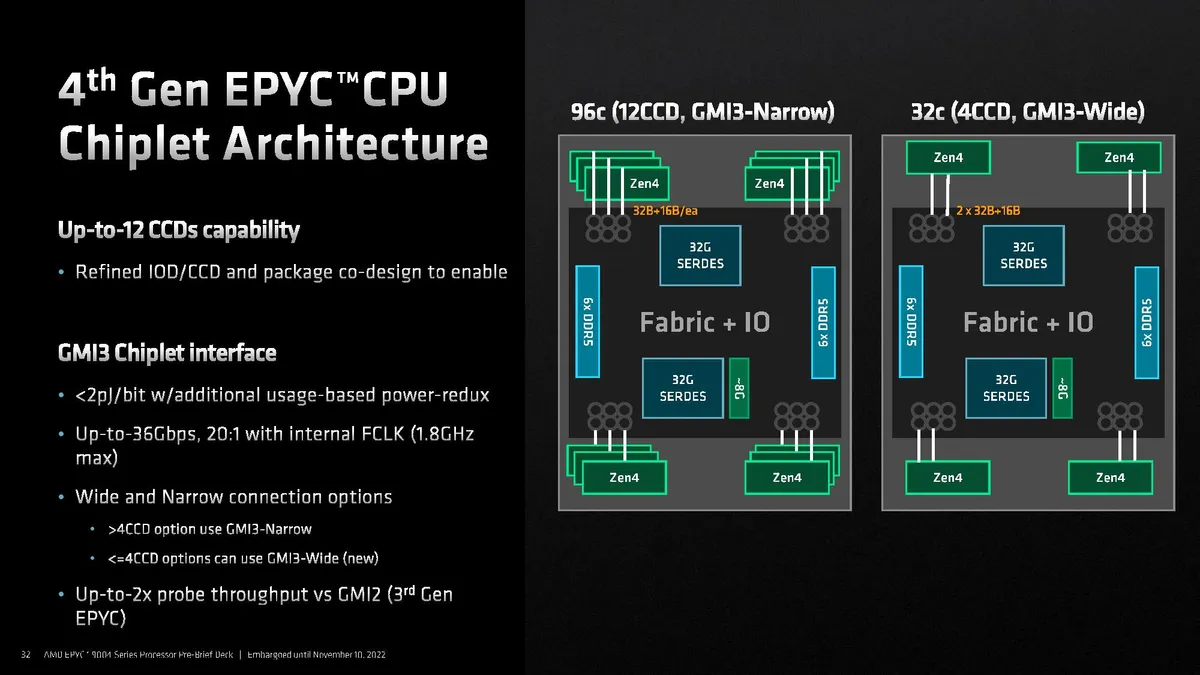


AMD leverages a similar chiplet-based design as we’ve seen with prior-gen EPYC, but moved to more performant GMI3 links between the 6nm I/O die (IOD), which ties the chiplets together and houses the DDR5 and PCIe 5.0 controllers, and the eight-core 5nm Core Complex Dies (CCDs).
AMD’s previous-gen EPYC had eight Global Memory Interconnect 2 (GMI2) links that supported 8 CCDs, whereas Genoa supports up to 12 CCDs. AMD uses the same IOD for all variants of the EPYC processors, but a different number of CCDs for various SKUs (we included the CCD counts in the table on the first page). As such, lower core-count models with four CCDs can have dual-GMI3 links (wide mode) with the IOD, a new capability that can offer advantages in some throughput-intensive tasks, while larger CCD arrangements use a single GMI3 link per chiplet (narrow mode).
As before, the links provide 32B read and 16B write bandwidth per fabric clock and consume 2 pj/bit (picojoules per bit).


AMD’s new Socket SP5 comes with vastly improved power delivery capabilities courtesy of improved voltage regulators and platform design, which we’ll take a closer look at on the following page. Other improvements include a new flexible Infinity Fabric topology that allows for expanded configuration options for OEMs.
As with Milan and other Socket SP3 EPYC platforms, the two sockets can be connected by either three or four PCIe-based Infinity Fabric links (G Links). A 3Link configuration allows one cross-socket link to be peeled off and dedicated to increasing I/O connectivity for the platform, like more NVMe or networking connections. As such, these links can use cables for custom configurations. However, with SP3 systems, these links are only present at the top of the server (“G” Links), thus requiring long cabling runs that add complexity when provisioning additional I/O on the back panel of the server. With Genoa, AMD added the ability to split those lanes off via cabling at either the top or the bottom of the socket to simplify cabling and improve signal integrity to the rear I/O. The lanes at the bottom of the socket area are referred to as “P Links.”
The transition to a new memory last happened eight years ago, so the move to DDR5 brings about new complexity at every layer of the design process. From the DDR5 memory controllers inside the processor to the traces, slots, redrivers, switches, and even the materials used in motherboard design, DDR5 has an impact that results in increased costs. So naturally, the payoff is doubled throughput, which can deliver massive improvements in bandwidth-sensitive workloads.
EPYC Genoa supports up to 6TB of DDR5 per socket, spread across 12 channels of DDR5 memory running at DDR5-4800 in one DIMM per channel mode (1DPC). AMD hasn’t yet defined the supported 2DPC speeds, but we’re told that will arrive in the first quarter of next year. Given that most motherboard designs are already space-constrained by cramming in 12 channels, AMD feels that qualified support for 1DPC is sufficient for launch.
The peak theoretical throughput for 12 channels of DDR5 weighs in at 460 GB/s, but the actual throughput will vary. In addition, DDR5 comes with higher latency than DDR4, but AMD says that Genoa’s internal pathways provide roughly the same effective latency as the DDR4-powered Milan chips. Overall, AMD says there is a ~13ns penalty for the Genoa implementation compared to Milan.


Compute eXpress Link (CXL) is an open industry standard with support from all the major silicon vendors, but it has just emerged over the last few years, and the first devices are finally making their way to market. As a reminder, the CXL 1.0 spec is an open industry standard that provides a cache coherent interconnect between CPUs and accelerators, like GPUs, smart I/O devices, DPUs, and various flavors of DDR4/DDR5 and persistent memories. The interconnect allows the CPU to work on the same memory regions as the connected devices, thus improving performance and power efficiency while reducing software complexity and data movement. This specification currently communicates over the PCIe 5.0 bus, but the CXL 3.0 revision of the spec has already charted a course to PCIe 6.0 support.
The CXL spec has matured rapidly, and CXL 2.0 arrived before widespread support for CXL 1.0 arrived in any meaningful quantities. This specification requires baked-in support at the SERDES level to enable low-latency connections — equivalent to the latency penalty of a single NUMA hop — to remote banks of memory.
As such, AMD had to intercept the new capabilities of the 2.0 spec late in the design stages for Genoa, essentially re-designing its SERDES to support the new features. That resulted in fast yet not-quite-complete support for CXL 2.0. As such, AMD terms its support for CXL as version 1.1+, a similar approach we’ll see with Intel’s Sapphire Rapids.
CXL supports three types of devices, but AMD has focused on adding the most robust support for the most important feature for the industry at large — the Type 3 devices that enable memory expansion. As such, Genoa ropes in the persistent memory and RAS reporting features from CXL 2.0 for Type 3 devices into its CXL 1.1+ implementation.
This capability allows users to address remote memory as local memory. In addition, Genoa allows multiple Type 3 devices to be aggregated into one interleaved NUMA node, and it also supports ‘headless NUMA’ nodes. Other features include QoS mechanisms to account for the latency delta between truly local memory and the CXL memory devices, along with support for AMD’s SEV/SNP security features to protect data.
For now, the leading-edge CXL memory expansion devices slot directly into the PCIe slot, but CXL Type 3 devices will evolve to network-attached memories in the future.
AMD’s SERDES now has two types of connections, with one type of SERDES port supporting the standard xGMI or PCIe interfaces while the other additionally supports more interfaces, like SATA and, more importantly, CXL.
AMD only supports CXL devices on the “P Links” described in the section above, meaning that the connections stem from the links at the bottom of the socket. As you can see in the diagram, AMD supports varying levels of connectivity in its SERDES based on the type of connection.
CXL support peaks at 16 devices in a single socket if they are spread across the x4 connections, but customers can also use x8 and x16 CXL connections. As such, customers can allocate up to 64 of the 128 available PCIe 5.0 lanes to CXL devices.
- MORE: Best CPUs for Gaming
- MORE: CPU Benchmark Hierarchy
- MORE: AMD vs Intel
- MORE: Zen 4 Ryzen 7000 All We Know
