Intel Lakefield 3D Foveros Hybrid Processors: Hot Chips 31 Live Coverage
Here at Hot Chips 31 Intel is unveiling more details about Lakefield processors using its new Foveros (Greek for "awesome") tech, a new 3D packaging technology that Intel uses to build new processors stacked atop one another. This is live coverage, so refresh your browser or return to the article for as-it-happens updates.
The concept behind 3D chip stacking is a well-traveled topic that has been under development for decades, but the industry hasn't been able to circumvent the power and thermal challenges, not to mention poor yields.
Chip stacking allows mixing and matching different types of dies, such as CPUs, GPUs, and AI processors, to build custom SOCs. It also allows Intel to combine several different components with different processes onto the same package. That lets the company use larger nodes for the harder-to-shrink or purpose-built components. That's a key advantage as shrinking chips becomes more difficult.
Intel says it built Foveros upon the lessons it learned with its innovative EMIB (Embedded Multi-Die Interconnect Bridge) technology, which is a complicated name for a technique that provides high-speed communication between several chips. That technique allowed the company to connect multiple dies together with a high-speed pathway that provides nearly the same performance as a single large processor. Now Intel has expanded on the concept to allow for stacking die atop each other, thus improving density.
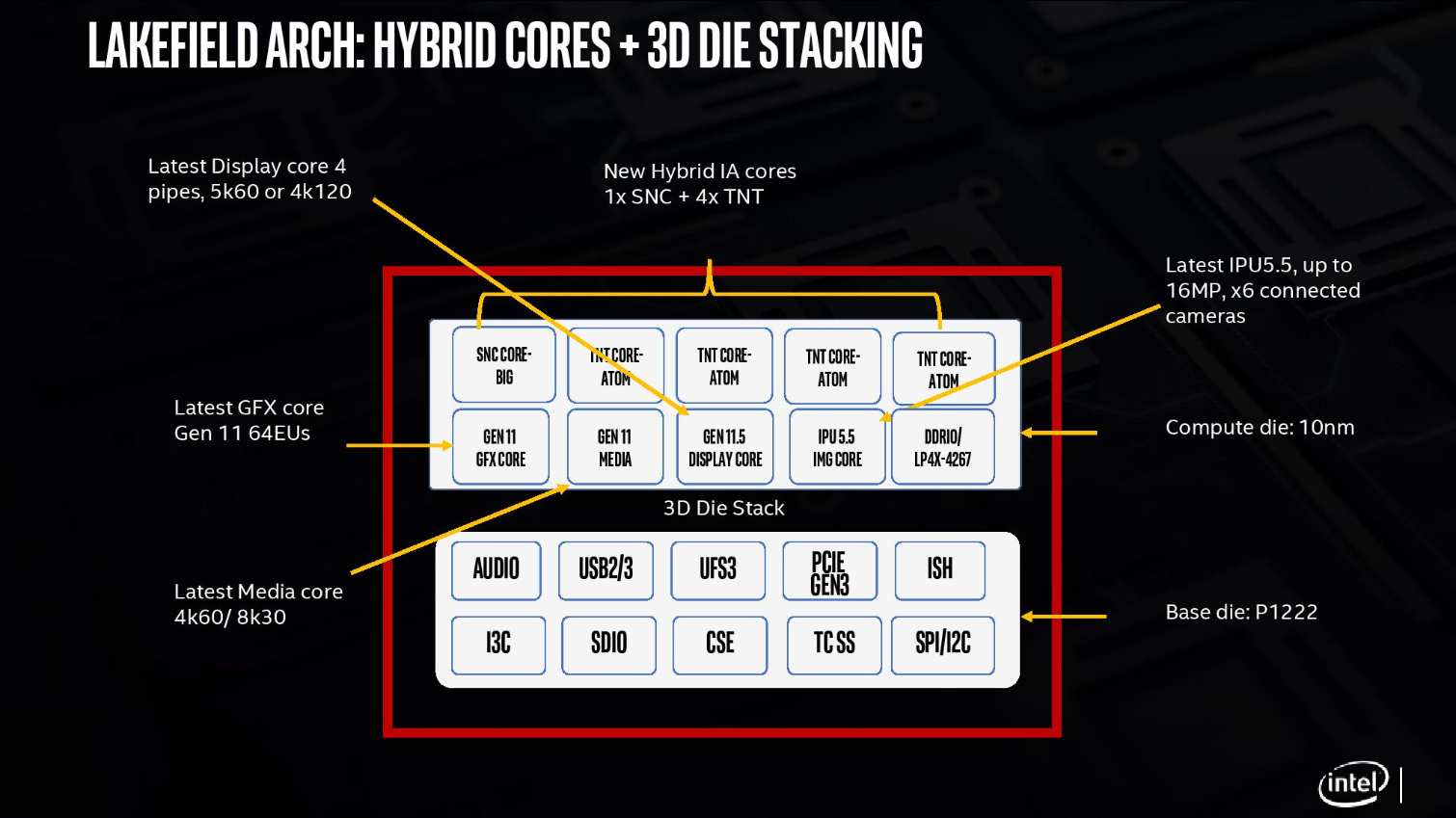
Lakefield processors are the first to come to market with Intel's new 3D chip-stacking technology. The current design consists of two dies. The lower die houses all of the typical southbridge features, like I/O connections, and is fabbed on the 22FFL process. The upper die is a 10nm CPU that features one large compute core and four smaller Atom-based 'efficiency' cores, similar to an ARM big.LITTLE processor. Intel calls this a "hybrid x86 architecture," and it could denote a fundamental shift in the company's strategy. Finally, the company stacks DRAM atop the 3D processor in a PoP (package-on-Package) implementation.
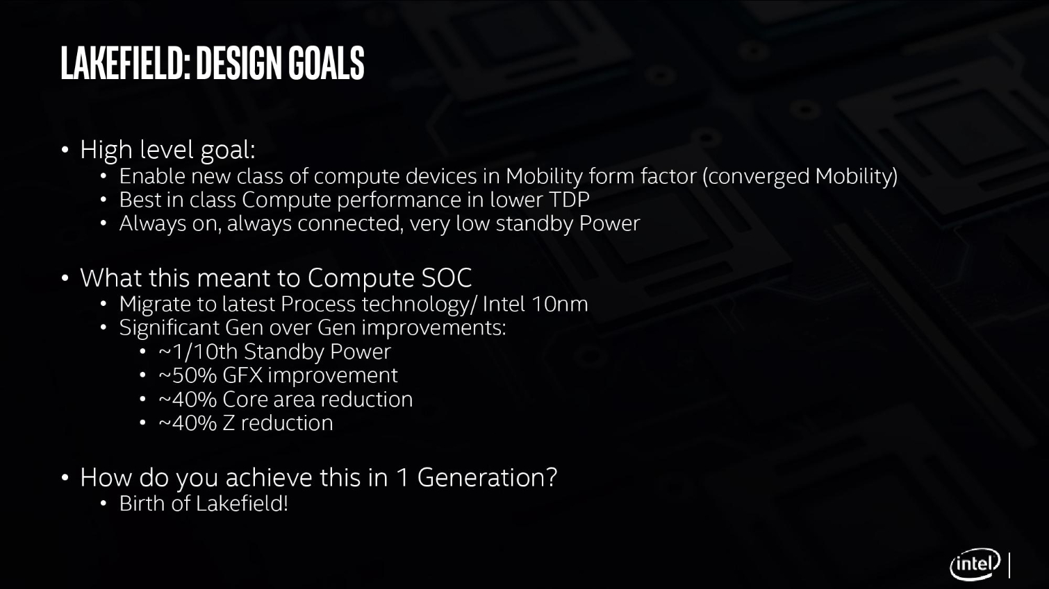
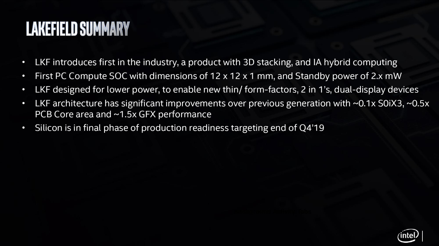
Lakefield enables new converged mobility form factors that are smaller than traditional PCs. Think super-thin, fanless, and low standby power in the 2 or 3 milliwatt range. Standby power had to go down 1/10th, and graphics power had to go up 50%. The motherboard area had to go down 40%, and thickness needed to be reduced by 40%. That required a profound change in the approach.
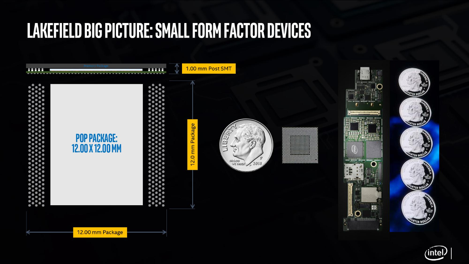
The speaker displayed a real Lakefield chip with three die: memory, CPU, and I/O dies. He also presented a full compute platform on a single-sided PCB that is incredibly small. That's the entire computer on a slim stick.
Get Tom's Hardware's best news and in-depth reviews, straight to your inbox.
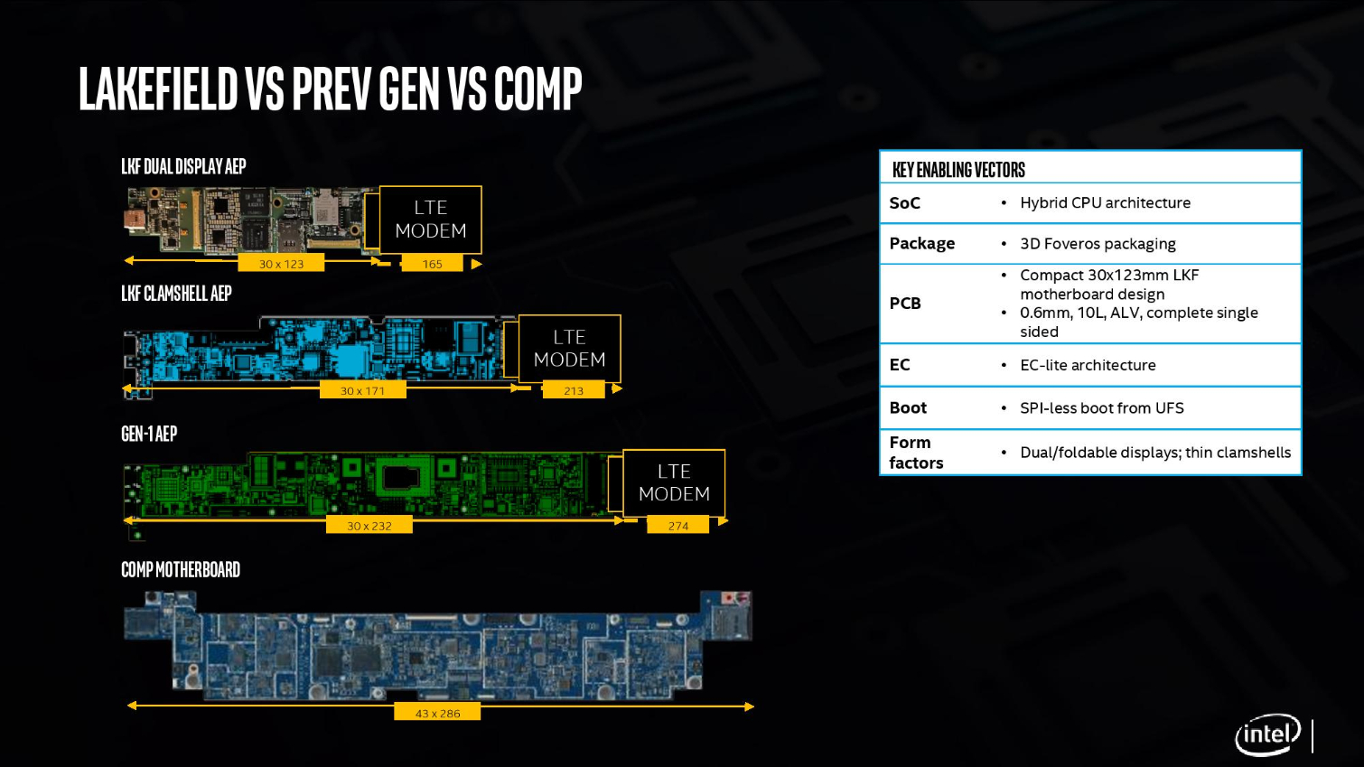
Here we can see the key enablers to creating the smallest motherboard Intel has ever made.
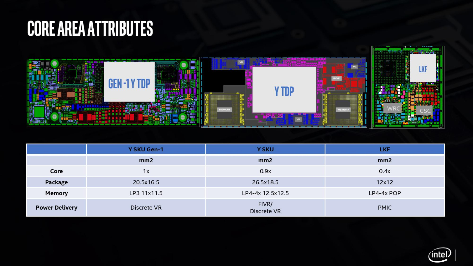
The board area of Lakefield is smaller than half the size of previous-gen boards, largely because of the smaller chip package. Instead of using FIVR for power delivery, Intel used PMIC. Actually two, one for the bottom die, and one for the top.
Here we see both die and their components. The top die has the CPU with one large core and four small Atom cores. This is called the compute die.
The bottom die is the base die. This has several I/O blocks.
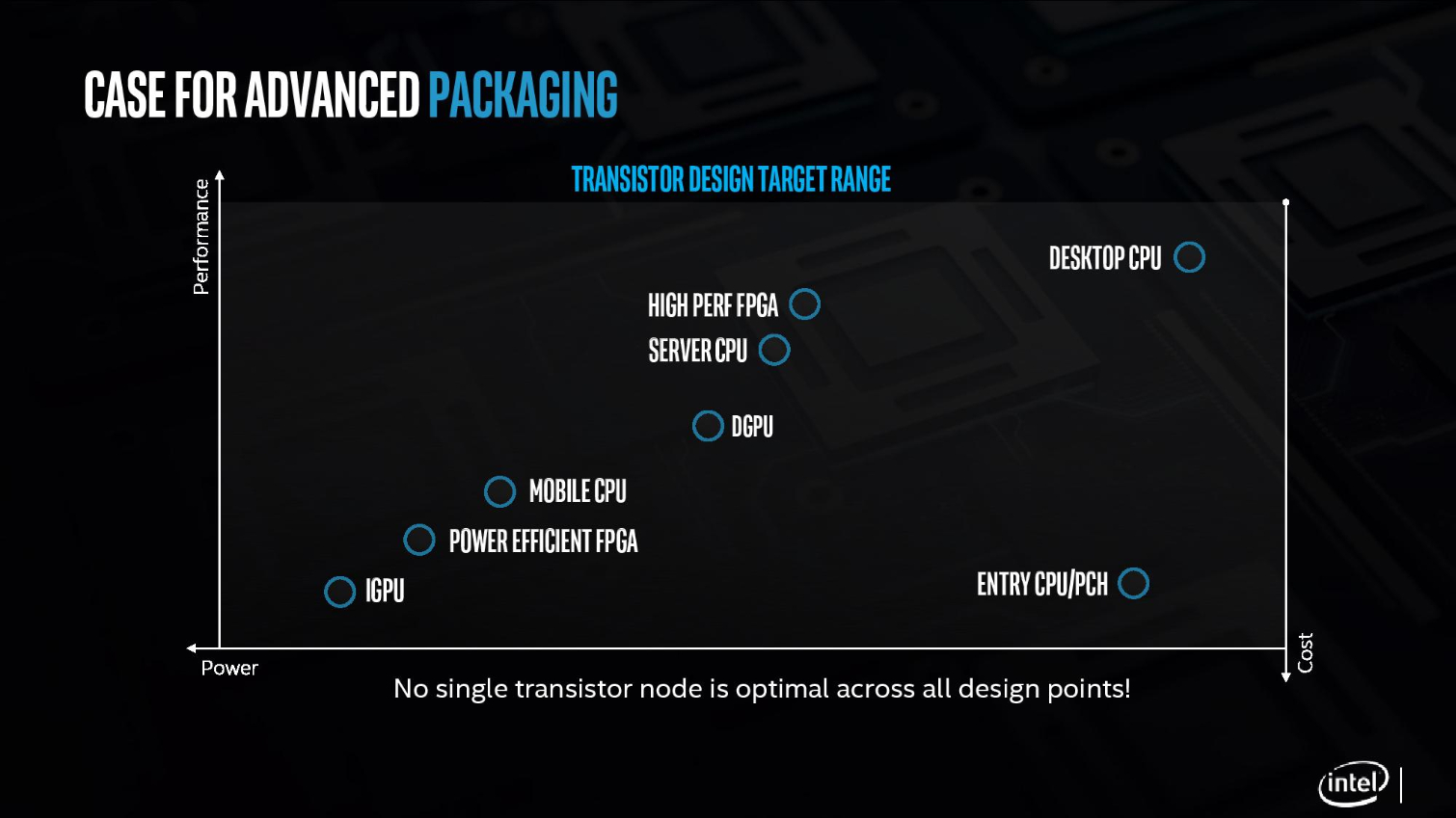
Different types of transistors offer different advantages for certain use cases. You can't build a single transistor to meet all these needs, so it's best to use two packages.
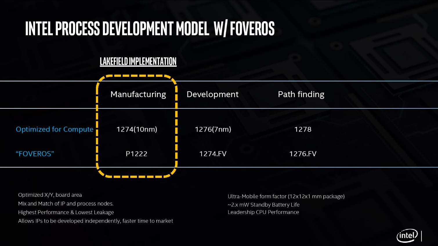
The low-leakage P1222 process was used for the base die, and 10nm for the compute die. Stacking the two die together behaves like a monolithic die. Intel will use 7nm for the compute die and 1274.FV for the base die in future models.
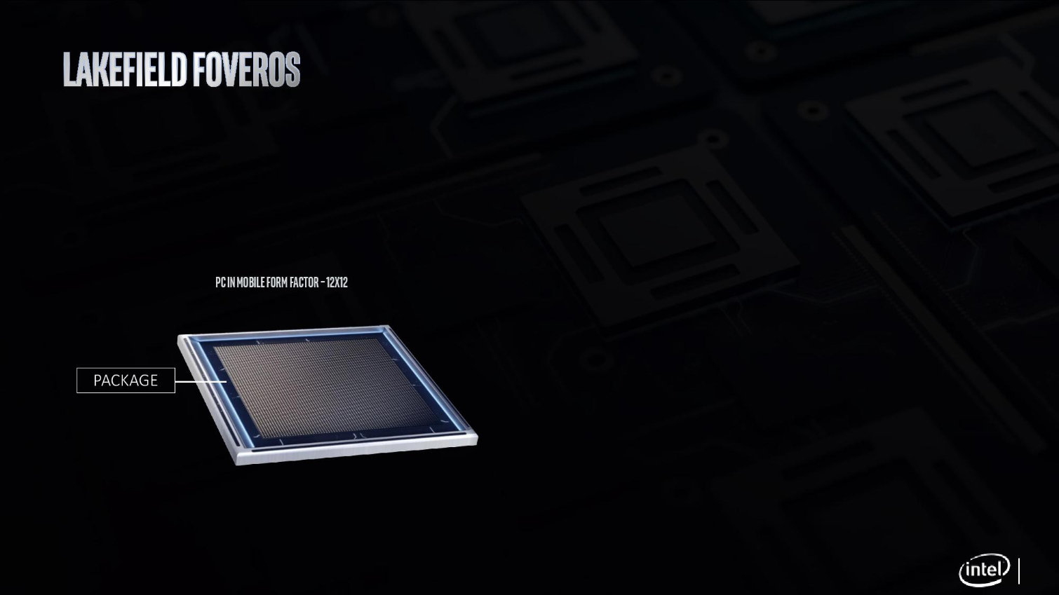
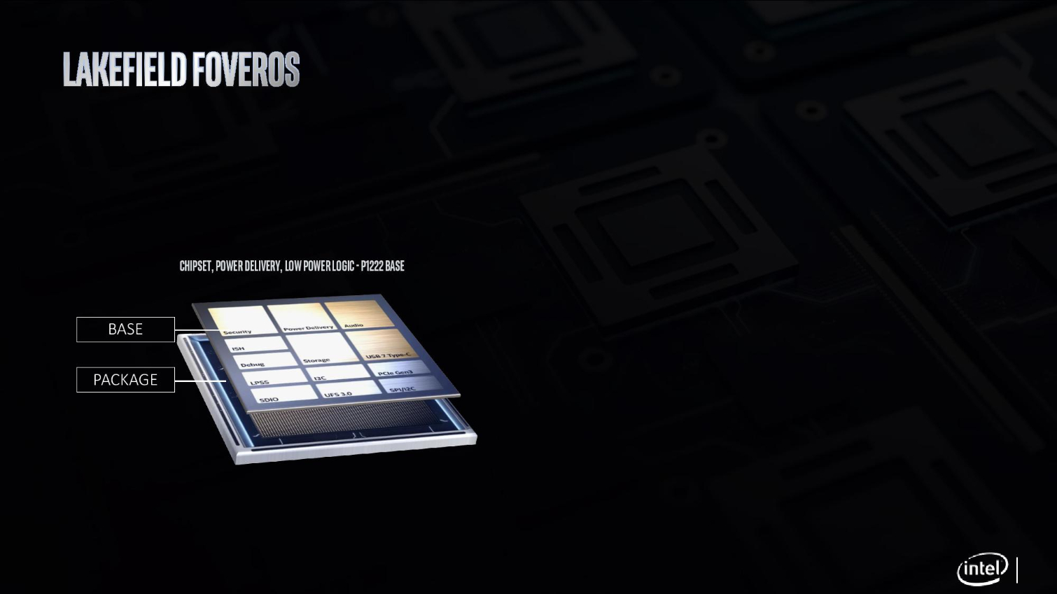
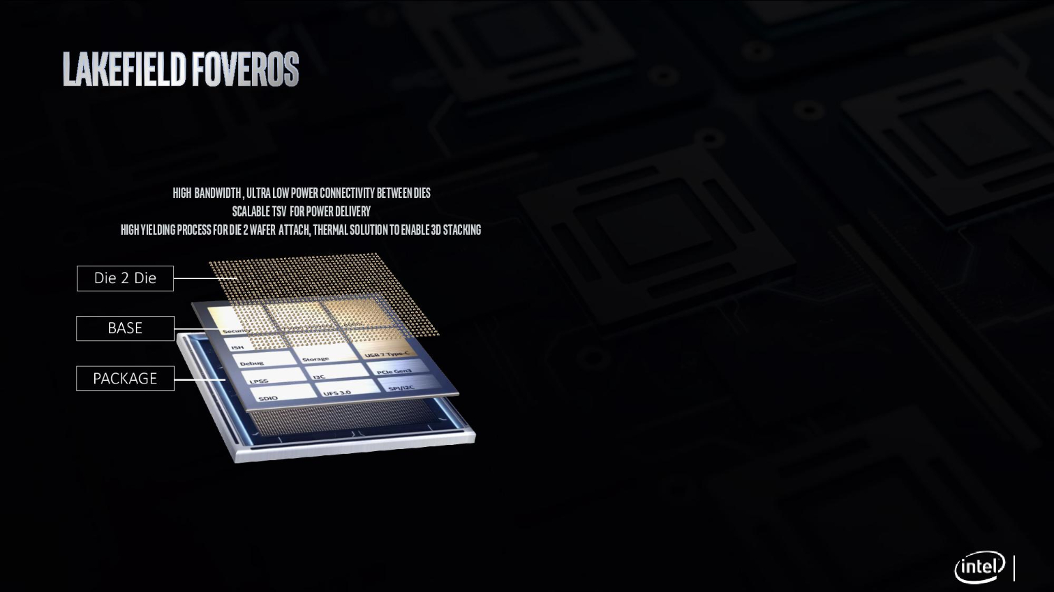
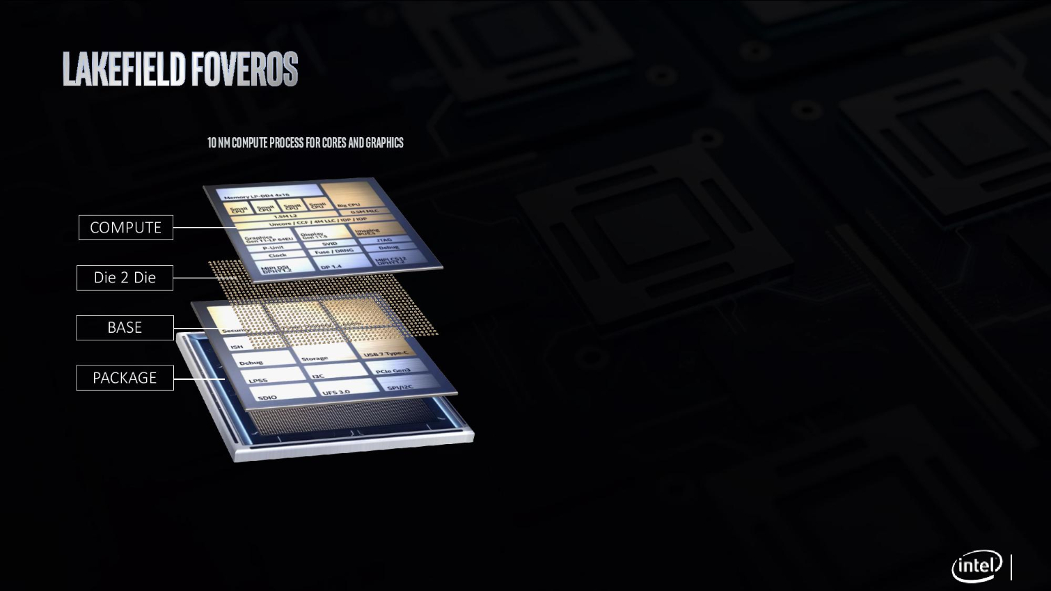
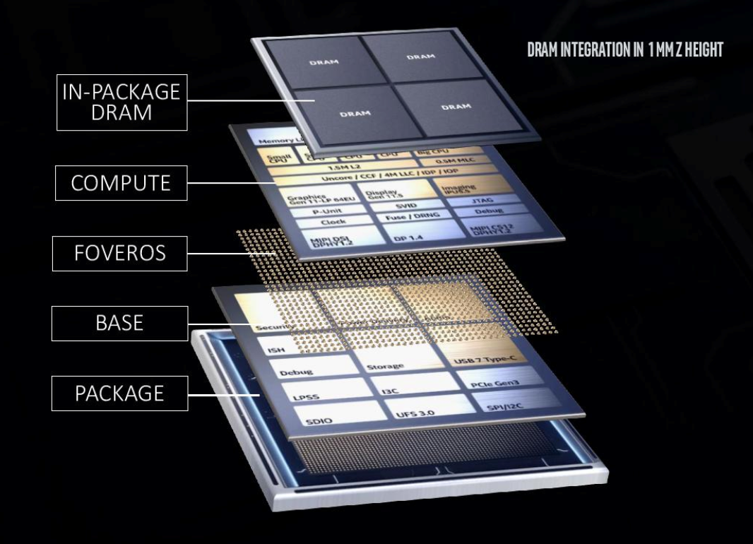
Everything that is not needed for compute goes on the bottom, then there is a die to die interlink, a thermal shield, and then a compute die. Finally, the DRAM is mounted to the top of the package.
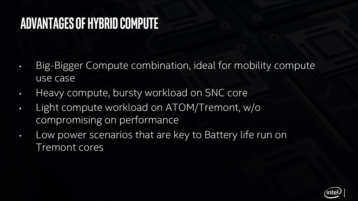
Hybrid architectures combine a big core for compute-heavy cores, while smaller cores handle light tasks. Sunny Cove is used for the big core, while Atom Tremont is used for the small cores.
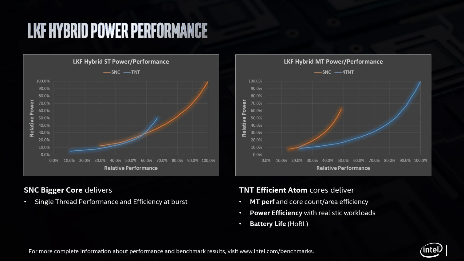
Blue is Tremont power consumption, and yellow is Sunny Cove power consumption. Both are plotted over single-threaded performance. This provides a broader range of both performance and efficiency. That gives a 50% gain in performance at higher TDP ranges, while Tremont is better in the lower ranges.
The second chart (left) plots the same metrics in multi-threaded workloads.
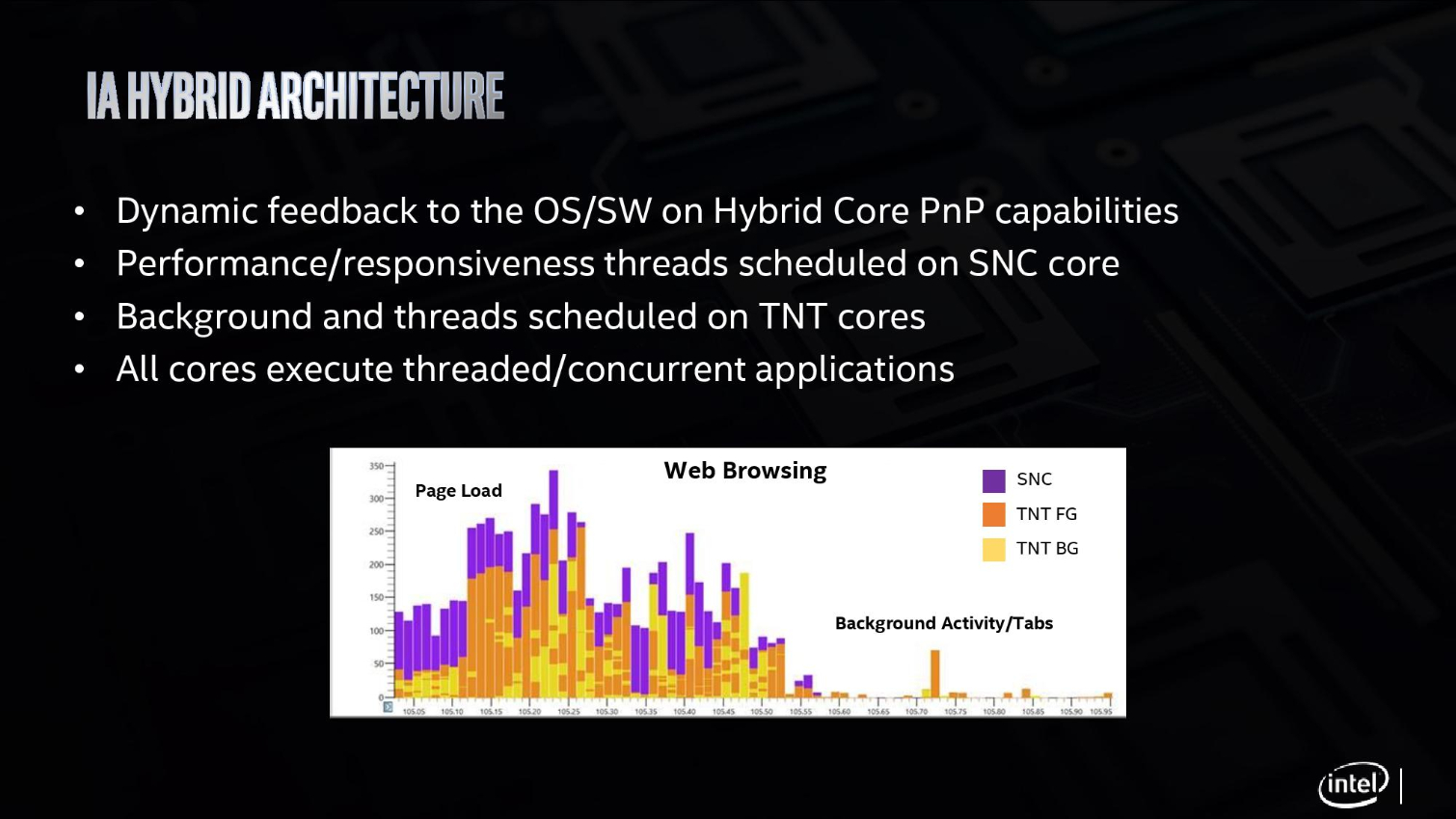
Here we can see how Intel moves the heavy and light workloads between the two types of cores. This requires some interaction from the software and operating system. Naturally, performance workloads go to the Sunny Cove cores, while background and light workloads go to Tremont.
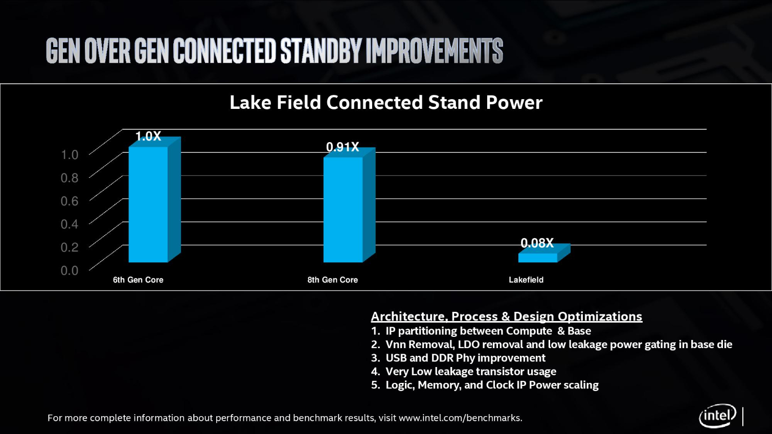
Reducing standby power was a big goal of the design. Here we can see that Lakefield uses 1/10th the power of 6th-gen Core chips when in standby.
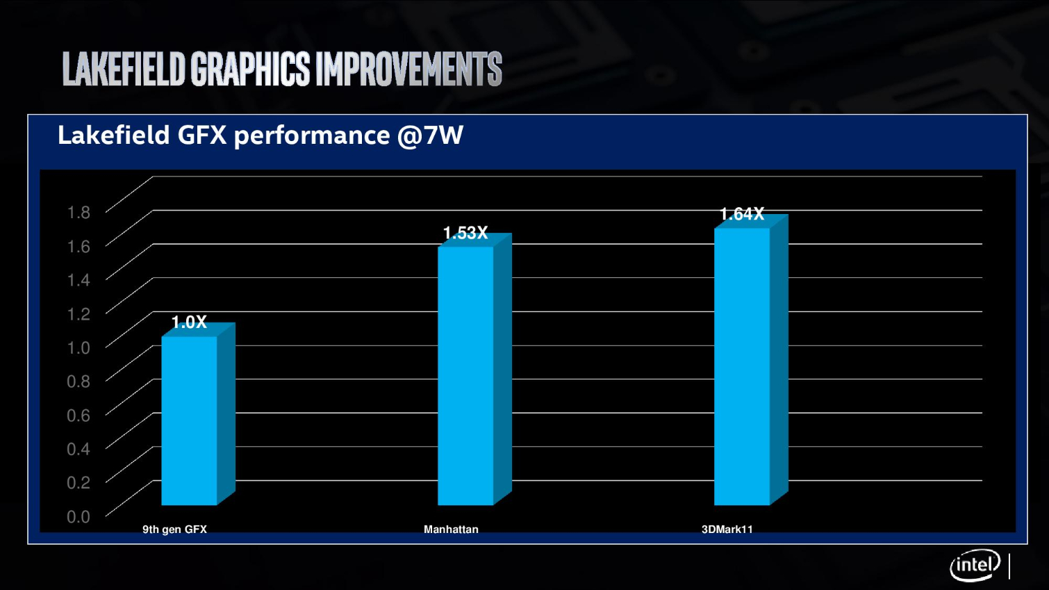
The chips use Gen11 graphics with 64 Eus. Here we can see big performance gains.
Lakefield is the first chips to deliver on all these design goals. The chips are targeted for the end of Q4 for production samples.
Intel is using 10nm+, the same process as Ice Lake. In terms of interconnects, Intel uses a 50 micron pitch for connections and a 20 micron pitch for microbumbs. Relaxed pitch improves yields on the first device.

Paul Alcorn is the Editor-in-Chief for Tom's Hardware US. He also writes news and reviews on CPUs, storage, and enterprise hardware.
-
mitch074 Ooooh... So, Intel reinvented big.LITTLE and confuses 2.5D and 3D ("real" 3D stacking would have tridimensional circuits; here you have layers that communicate with one another, so 2.5D). Awesome indeed.Reply
Meanwhile, ARM already moved to DynamIQ. -
exroofer Soooo..... is this a 1 core, or a 5 core or.........Reply
So they then put 6 or 8 or w/e of these on one chip?
Because THAT would be interesting. -
bit_user Reply
I'd have thought it would be fairly low-end stuff. But, that 64 EU GPU says otherwise.nufelevas said:This is aimed only at the arduino/arm/phone/atom market, or also at the desktop PC?
So, basically, ultra-thin laptops and 2-in-1 convertibles. Not desktops, though. -
bit_user How much DRAM gets stacked in-package? That doesn't seem big enough to be all of the system's memory...Reply
Edit: I'm reading 4 - 8 GB. So, yeah, that's probably all of it. -
Growle May be a good thing for future gaming consoles, "extra-small" form factor PCs, and smart pillows.Reply
I like the sound of Tiny Form Factor though. -
JayNor Is that LTE chip from Intel?Reply
There are reports that this chip is being used in Microsoft's Centaurus. It appears to be a foldable notepad 2 in 1. I'd rather use something like that than a cellphone ... seems more useful to me. I wonder does the Apple deal prevent Intel from putting their LTE chips in this format.
https://www.extremetech.com/computing/293787-microsofts-dual-screen-surface-could-launch-in-2020-run-android-apps -
bit_user Reply
As I'm sure you know, smaller can sometimes mean more expensive, like how Apple's Airtops are more expensive than their baseline Macbooks.Growle said:May be a good thing for future gaming consoles, "extra-small" form factor PCs, and smart pillows.
I like the sound of Tiny Form Factor though.
It seems pretty clear to me that this is not going to be their cheapest SoC part. I don't expect to see it in Chromebooks (other than maybe a couple higher-end models), for instance.
And it's definitely not for gaming consoles, other than maybe portable ones like Nintendo Switch.
If you were building a PC (or even a NUC), there's no good reason to use such a highly-integrated, low-power product, especially having only one "fast" core. -
GetSmart Reply
Well, some Chromebooks also featured more expensive Intel's mobile Core SoCs (not just cheaper SoCs from Intel's Atom lineage), thus would not count that out either.bit_user said:It seems pretty clear to me that this is not going to be their cheapest SoC part. I don't expect to see it in Chromebooks (other than maybe a couple higher-end models), for instance.
