Intel’s Massive Sapphire Rapids Processor Poses for Camera (Updated)
Sapphire Rapids A2 silicon in the flesh

Update 2/4/2020 6:00pm PT: Added additional pictures of delidded processor. We've added additional analysis below.
Intel's CEO recently confirmed that the company had started to sample its next-generation Xeon Scalable 'Sapphire Rapids' processors to partners, so it isn't particularly surprising that the first images of the CPU have emerged, proving that the chip is in the hands of Intel's partners.
Being a sample rather than a commercial product, the processor is marked as Intel Confidential and features the QVV5 sSpec, along with a 1.30 GHz frequency. The image was published by YuuKi_AnS, a known hardware leaker who sometimes has access to unreleased chips.
We confirmed the CPU's validity with an independent source with knowledge of the matter, who identified the device as a 28-core Sapphire Rapids A2 sample that Intel sent to partners several weeks ago.


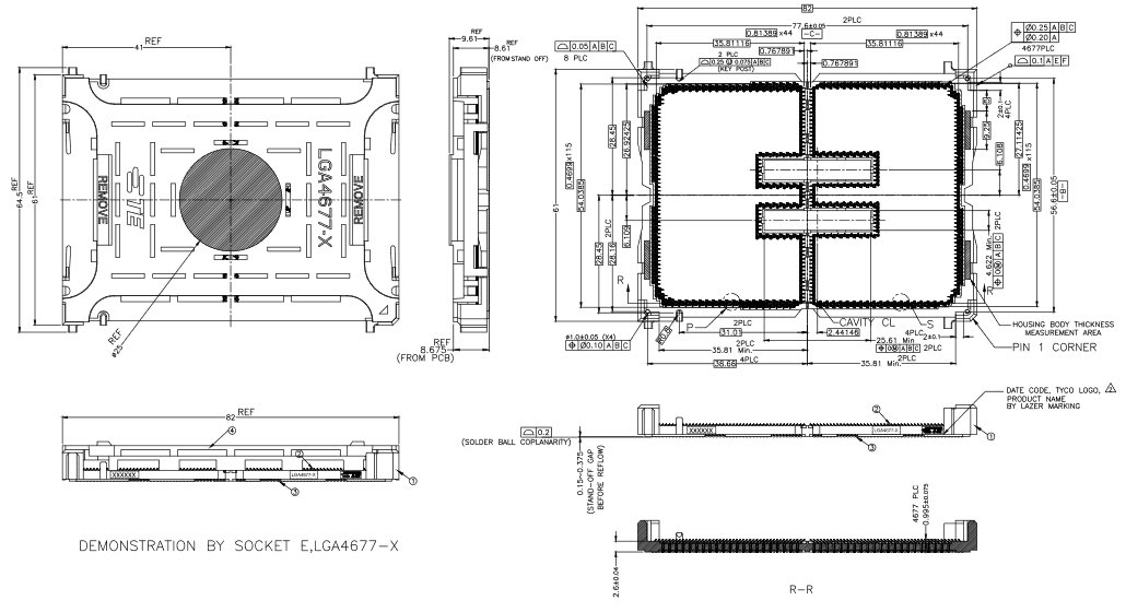
The backside of the chip looks exactly like it should, according to the blueprints of Intel's 4677-pin socket (made by TE Connectivity) that have floated around since at least October 2019. This might be considered more proof that the CPU is indeed a Sapphire Rapids sample in LGA4677 packaging.


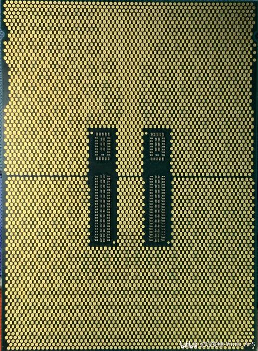
We understand that the A2 sample features 28 cores, but it is unclear whether the processor — which is made using Intel's 10nm Enhanced SuperFin process technology — uses a multi-chip-module (MCM) design or one monolithic die. The heat spreader on the CPU has one big bulge that can cover more than one chiplet.
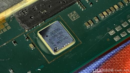
Update: YuuKi_AnS has published a photo of the delidded Sapphire Rapids processor revealing what is under the hood of the CPU. The Sapphire Rapids sample apparently carries four dies and an Altera Max 10 FPGA (which is probably used for startup/initialization purposes).
Using TE’s blueprint of Intel’s 4677-pin socket, we can estimate that an LGA4677 processor package measures slightly less than 72.4x54 mm, therefore occupying ~3,910 mm2. Using some very rough napkin math, we can estimate that the four dies occupy a significant portion of that area, which makes these chiplets fairly large.
Since we're allegedly looking at a 28-core CPU, each die should only have seven active cores. Unless Intel decided to pack enormously large caches and loads of special-purpose accelerators into its Sapphire Rapids chiplets, we can gather that each chiplet integrates a significantly higher number of cores (14, according to YuuKi_AnS), but at this point many of them are disabled. In any case, the image shows that Intel’s Xeon Scalable ‘Sapphire Rapids’ CPU uses four dies presumably interconnected using EMIB technology. Since it is inherently easier to make smaller chiplets than one large die, it should be easier for Intel to ramp up the production of its next-gen CPU for data centers and supercomputers.
Get Tom's Hardware's best news and in-depth reviews, straight to your inbox.
It's noteworthy that the new alleged Intel Sapphire Rapids A2 sample doesn't look like another assumed sample of a Sapphire Rapids CPU, of which a picture emerged last year. The backside of the processor from December actually looks like the backside of an LGA4189 CPU, which means that it might not be a Sapphire Rapids in an LGA4677 package. Meanwhile, since the front side of the device has two bulges and does not look like the front side of Intel's Cooper Lake or Ice Lake-SP CPU, it is indeed an unannounced processor that allegedly uses an MCM design.
One thing to note about the current leak is that YuuKi_AnS added two stickers to his pictures. The stickers carry the G14056-002 part number, which matches the part number of Intel's Xeon Phi 7120P. Obviously, the addition does not add any credibility to the leak, but since the CPU packaging corresponds to the LGA4677 blueprints and we have another confirmation from an independent source, it is highly probable that we are dealing with a Sapphire Rapids sample.

Anton Shilov is a contributing writer at Tom’s Hardware. Over the past couple of decades, he has covered everything from CPUs and GPUs to supercomputers and from modern process technologies and latest fab tools to high-tech industry trends.
-
greatmaharg " inconsistent performance from 4 glued-together desktop die." - Intel marketing dept.Reply -
rtoaht Reply
...and they were right. Naples provided inconsistent performance due to the was the memory subsystem was broken down in 4 chiplets. Due to NUMA, whenever one chiplet needs to access the non-local memory (located in other chiplet) via infinity fabric, the performance tanked and it also came with latency penalty. 2nd gen Rome significantly improved (but not fully resolved) this issue with better memory architecture and larger cache. Finally, "glue" is actually a technical term which was previously used by AMD marketing department to deride Intel's old dual core CPUs.greatmaharg said:" inconsistent performance from 4 glued-together desktop die." - Intel marketing dept. -
spongiemaster Reply
And Intel was factually correct about the inconsistent performance, though the glue part was unnecessary. AMD acknowledged this when they released the game mode for Threadripper that disabled one of the CCXes.greatmaharg said:" inconsistent performance from 4 glued-together desktop die." - Intel marketing dept. -
spongiemaster Reply
The Pentium division bug?PaulAlcorn said:Any guesses on what that FPGA is there to fix? :p
