
Intel began telling its Tiger Lake story last week at its Architecture Day 2020, but today it shared more details of the upcoming chips at Hot Chips 2020. That includes the first picture of a quad-core Tiger Lake die, and more information on its enhanced ring bus interconnect between the cores. This new design will be key for Intel as it looks to wrest the performance and power consumption advantage in mobile laptops from AMD's potent Ryzen 4000 Renoir processors.
As a quick refresher, the Tiger Lake processors mark the debut of Intel's 10nm SuperFin transistors. Intel bills these optimized transistors, which are an iteration of the existing 10nm, as delivering the performance improvement typically expected of a new node. Highlights include roughly 15-20% performance improvements at the same voltages/clocks in some areas, and much higher peak clock speeds - likely in the range of 5GHz for mobile parts. You can learn all about those new advances here.
Intel pairs those optimized transistors with new Willow Cove cores, increased cache capacities, tuning for high speed, Intel's Xe LP graphics (which deliver up to twice the performance of previous-gen Intel iGPUs), and support for up to LPPDR5-5400 memory and PCIe 4.0. Altogether, Intel says Tiger Lake has a 'greater than generational' level of performance improvement.
With those details out of the way, on to the new stuff (please see the above two pieces for more details about Tiger Lake).

Here we can see the image of the die that Intel shared during its presentation at Hot Chips 2020. Intel hasn't specifically marked the die image with the various components, but the large blue area to the lower right-hand corner is likely the Xe LP graphics unit (comprising roughly 33% of the die). That isn't a bad investment in die area if Intel lives up to its claims of doubled graphics performance at any given power level.
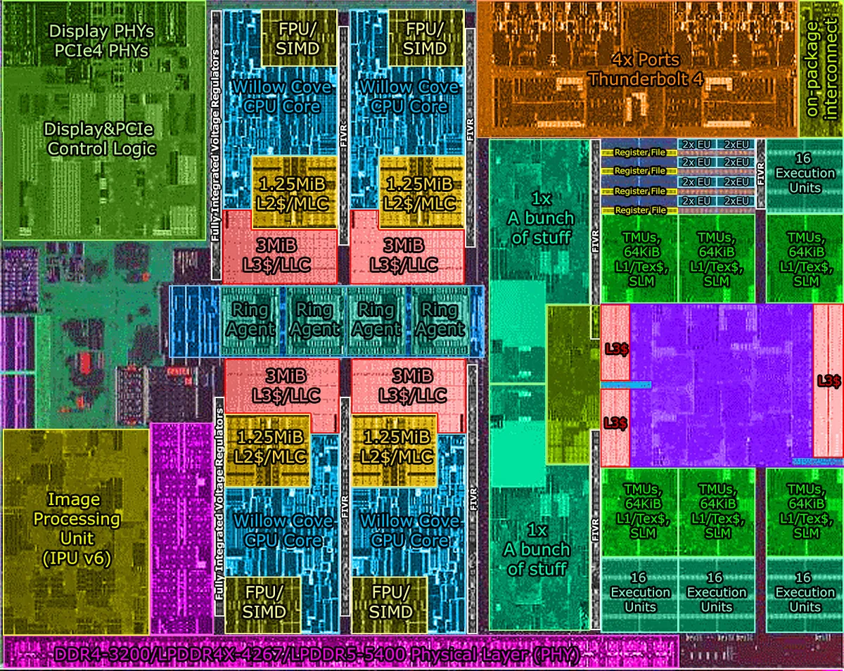
Here we see an *unofficial* annotated die image by silicon detective @Locuza_, who specializes in decoding complex die shots of processor microarchitectures. As such, do note there is room for error in this diagram, but it does align with our general expectations and analysis of the die.
To the left-center of the die, we see four large orange clusters that appear to be the L1, L2, and L3 cache structures, with the rest of the cores extending to the top and bottom of the die. Further to the left, we spot the system agent and I/O interfaces. The ring agent in the center of the image connects the iGPU, caches/cores, and system I/O blocks. Intel brought Thunderbolt 4 mostly on-die with the original Ice Lake processors, and we can see that continue with the large dedicated die area in the upper right of the diagram.

Here we can see a more detailed SoC diagram than Intel has shared previously, but it's important to remember that these diagrams are almost never adjusted for scale or actual placement of the structures on the die. Intel says this diagram shows a four-core device for illustration purposes, perhaps hinting that models with higher core counts could come in the future. Intel says it will share more on core counts at launch.
Intel calls out its new increased cache capacity for its L2 (MLC) and L3 (LLC), which now weigh in at 1.25MB and 12MB, respectively. Intel has used inclusive caching implementations for its Skylake-based chips, but those topologies require data held in the private L2 cache to be replicated in the shared L3 cache. Intel increased L2 capacity this time around, which would have resulted in an untenable 5MB of copied data to be held in L3 cache. As such, the company moved to a non-inclusive scheme that doesn't require a copy of L2 data in the L3 cache, thus making room for larger working sets in the shared L3 cache.
We also see the support for LPPDRx-4267 memory on the first Tiger Lake models, and that increased throughput will help feed the bandwidth-hungry Xe LP graphics engine. Even though it isn't activated yet, Intel's plumbed-in support for DDR5 is important - this is a sign of the fundamental changes the company has said will reduce its time to market with new I/O options.
Case in point: PCIe 4.0. AMD beat Intel to PCIe 4.0 for both the desktop PC and server markets, highlighting a critical weakness in Intel's chips. While AMD brought PCIe 4.0 to its desktop and server chips, it chose to stay at PCIe 3.0 for its Ryzen 4000 "Renoir" mobile chips. That gives Intel the first mobile CPU processor with PCIe 4.0 (which Intel pointedly calls out in its slides). Notably, PCIe 4.0 is considerably more power hungry than PCIe 3.0, but Intel has taken a holistic approach to reducing total SoC power consumption.

Intel moved to the dual ring bus microarchitecture, though this varies significantly from the older dual ring busses found on high core-count Skylake-X dies of yore. In this design, each stop serves both bi-directional rings, meaning Willow Cove's dual ring bus is essentially two ring busses wrapped within one another. This approach doubles the coherent fabric's bandwidth, which is usually twice the memory bandwidth (172GB/s in this case).
However, while boosting the throughput between the different processor elements, like cores and I/O interfaces, promises much more performance, it can also lead to increased power consumption. Intel's presentation outlined many of the techniques the company used to reduce power consumption while still ensuring a tangible boost to performance.
Power gating via separate power domains controlled by Dynamic Voltage/Frequency Scaling (DVFS) techniques that allow the chip to run some elements at reduced clock speeds, or turn them off entirely, based on usage. Intel split its execution cores, fabric, iGPU, and memory (cache) interfaces into different power domains, allowing them to be selectively shifted into different levels of performance based upon the workload, as outlined in the slide deck above. These DVFS transitions are managed in hardware, thus eliminating the latency associated with OS-issued frequency transitions. AMD has long touted its 25ms response time for these types of frequency transitions, but Intel hasn't shared specifics yet.
These features allow the SoC to dynamically allocate power to the elements that need more power for any given workload, thus boosting aggregate performance. For instance, by reducing the fabric bandwidth (and thus power) during a compute-heavy CPU workload, the SoC can feed the CPU cores more power, thus boosting overall performance. Intel says this approach allowed it to simultaneously increase both the peak performance and efficiency of the design.
Here is the remainder of Intel's Hot Chips 2020 Tiger Lake slide deck, but much of this was previously disclosed. As mentioned, you can head to our Intel's Tiger Lake Roars to Life: Willow Cove Cores, Xe Graphics, Support for LPDDR5 and Intel's Path Forward: 10nm SuperFin Technology, Advanced Packaging Roadmap articles for more details.


