Intel's Tiger Lake Roars to Life: Willow Cove Cores, Xe Graphics, Support for LPDDR5
10nm SuperFin to the rescue.
Intel made a dizzying array of announcements at its Architecture Day 2020 (full breakdown here). Still, its disclosures around its new Tiger Lake architecture with Willow Cove cores and its accompanying Xe LP graphics are arguably the most interesting, particularly because they will come in new laptops by the end of 2020 to fend off AMD's Ryzen Mobile processors. That's a desperately needed counter for Intel as AMD continues to make inroads in the high-performance notebook market while it simultaneously chomps away market share on the low end.
And Tiger Lake looks like a worthy adversary, at least from afar. Intel's announcements don't cover the specs for actual shipping silicon, but the architectural design certainly looks promising: The new Tiger Lake chips come with a revamped 10nm SuperFin transistor technology, higher frequencies than Ice Lake, a rebalanced cache hierarchy to improve performance, dual ring bus fabric, new security enhancements, support for LPDDR5-5400 in the future (LP4x-4267 for now), and the PCIe 4.0 interface, and Xe LP (Low Power) graphics, among many other improvements.
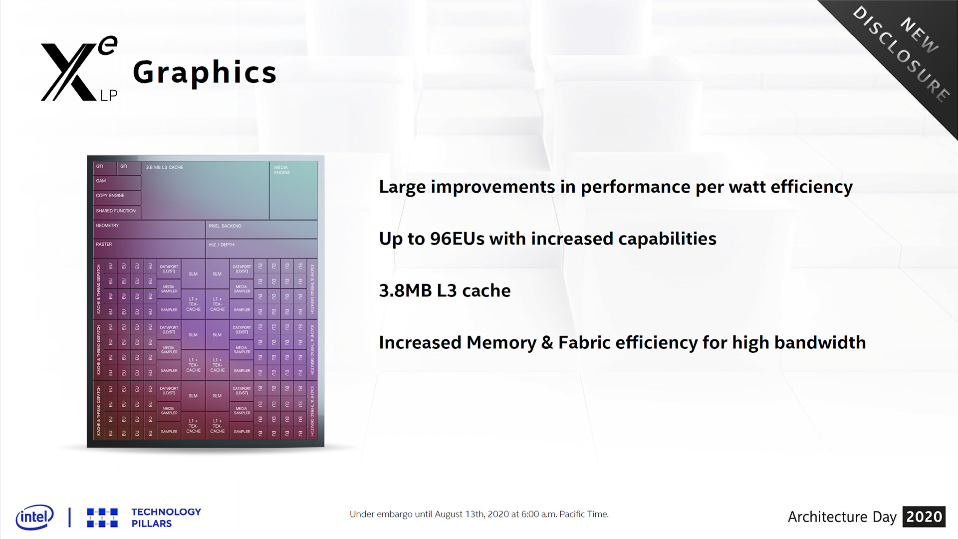
Don't be fooled by the "Low Power" in the Xe graphics branding, though. The Xe LP graphics engine promises up to twice the performance of the previous-gen Gen11, addressing a key sore point in Intel's lineup compared to AMD's capable 7nm "Renoir" Ryzen Mobile processors with Vega graphics. Intel's Xe LP comes with a significantly revamped architecture that merits its own further inspection, which we have in our Intel Drops XE LP Graphics Specs deep dive. The net-net is that the engine comes with up to 96 execution units (EU) and 'significant' performance-per-watt efficiency improvements over the previous Gen11 graphics, which implies twice the performance at lower power compared to Intel's Ice Lake.
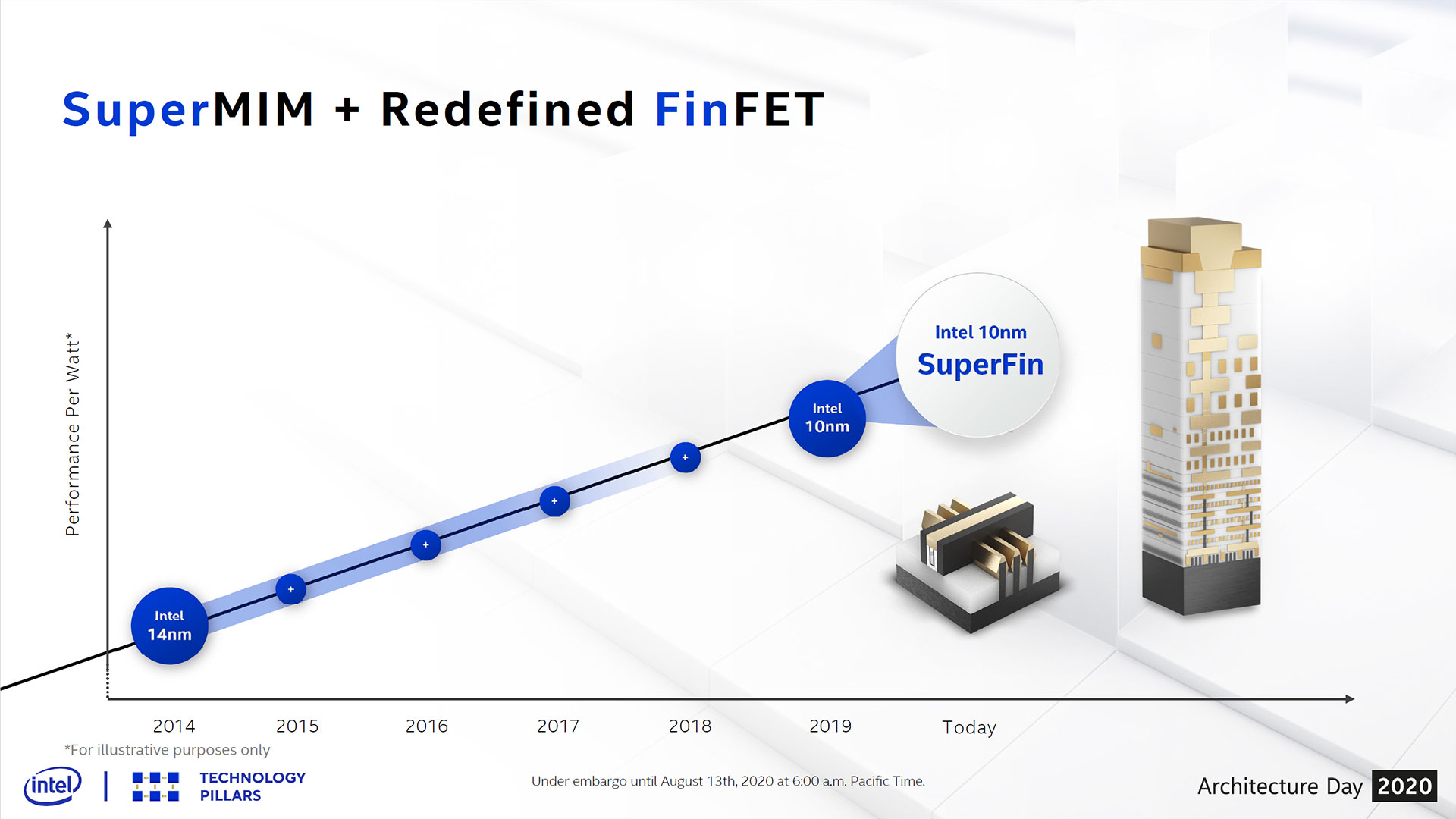
Much like the Tiger Lake CPU cores, a big part of Xe LP's performance improvement comes courtesy of Intel's 10nm SuperFin transistors. First, it's important to know that after four "+" revisions to its 14nm node (each + represented an improvement to the node), Intel has finally decided to discard the "+" branding. Due to rampant industry confusion about the naming scheme, including confusion among Intel's own teams, the company will now assign a new unique name to each process node. "10nm SuperFin" marks the first outing for its new terminology, but Intel says the node is the equivalent of a 10nm+ revision.
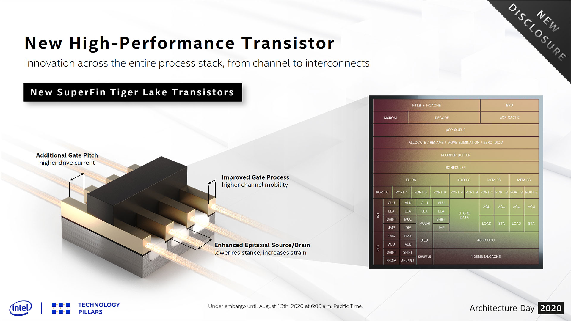
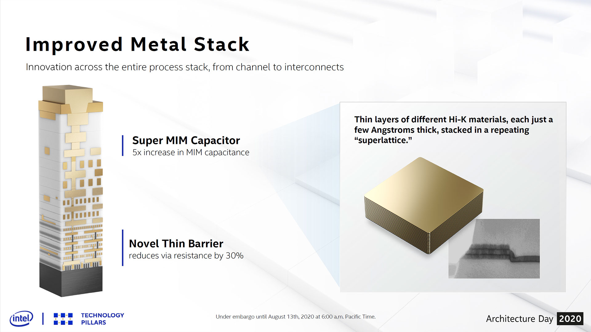
The 10nm SuperFin transistors have what Intel calls breakthrough technology that includes a new thin barrier that reduces interconnect resistance by 30%, improved gate pitch so the transistor can drive higher current, and enhanced source/drain elements that lower resistance and improve strain. Intel also added a Super MIM capacitor that drives a 5X increase in capacitance, which helps reduce vDroop.
The new 10nm SuperFin transistors merit their own piece with deeper analysis, which you can find here, but the key takeaway is that Intel says they deliver the same amount of performance uplift that the company would normally expect from a whole series of intra-node "+" revisions, but with just one iteration. In fact, Intel claims these transistors mark the largest single intra-node improvement in the company's history. The changes don't impact density, but have a big impact on performance.
With those process improvements at hand, Intel turned its eye to the Willow Cove microarchitecture found in the Tiger Lake chips. Intel says that instead of making drastic microarchitectural changes that would improve instruction per cycle (IPC) throughput, it instead focused on tuning the circuits of the existing Sunny Cove architecture to run at higher clock speeds. As a reminder, Intel designed the Sunny Cove architecture with a "deeper, wider, smarter" ethos that yielded up to a 15% to 18% IPC performance improvement over the Skylake architecture.
Get Tom's Hardware's best news and in-depth reviews, straight to your inbox.
However, while Intel says it did gain "some" IPC improvement for Willow Cove, it says the lion's share of performance improvement comes from tuning for higher clock speeds at lower power. That should improve per-core performance while preserving battery life in the 10-30W notebooks these chips are destined for (at least for now, we might see 45W and perhaps higher models in the future).
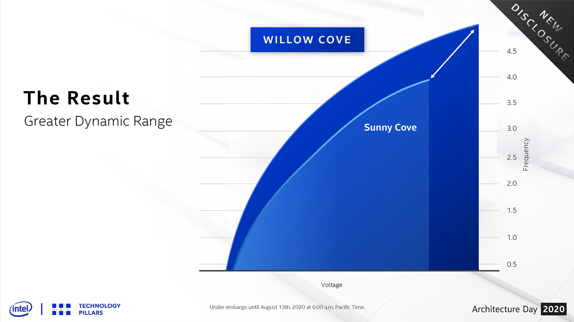
Overall, much of Tiger Lake's improved performance comes courtesy of the larger dynamic frequency range of the 10nm SuperFin transistors. The new transistors offer higher clock speeds at any given voltage, and can operate at a lower voltage at any given frequency. The transistors also have a greater dynamic range from the Vmin to Vmax (minimum/maximum voltage), and Vmax extends further than found with the original 10nm transistors. By tuning the architecture to exploit the full dynamic range of the transistors, Intel claims Tiger Lake offers both higher maximum frequencies in thermally-unconstrained use and is faster and more efficient in TDP-limited environments. Intel says the culmination of the tuning imparts a greater-than-generational performance improvement over the Sunny Cove cores present in Ice Lake.
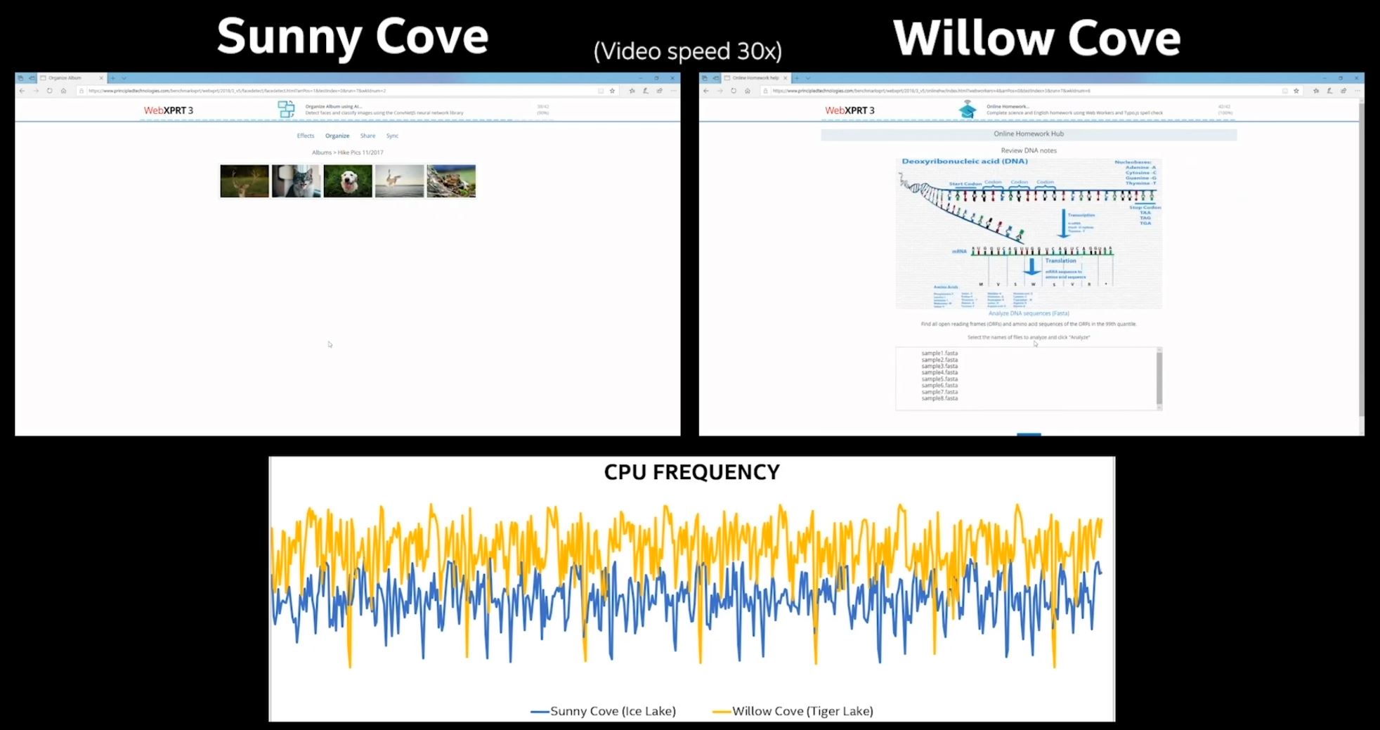
Web browsers represent one of the quintessential examples of a lightly-threaded workload that's highly dependent on per-core performance. Intel demoed Tiger Lake running the WebXPRT3 benchmark at both higher frequencies and lower power than the Sunny Cove cores found in the previous-gen Ice Lake chips. Intel confirmed that these measurements only include the single highest-boosting core in the system. That means it's possible that some of the uplift, which Intel says occurred at the same power, comes from some of the other power-saving measures that should allow better power balancing, as we'll outline below.
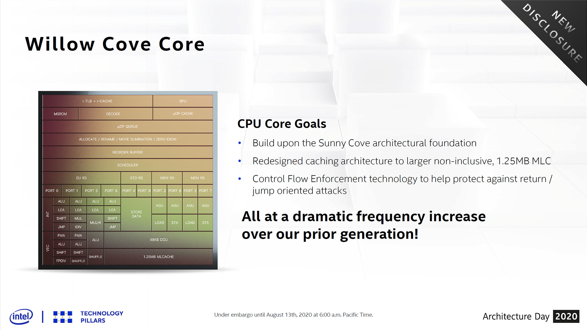
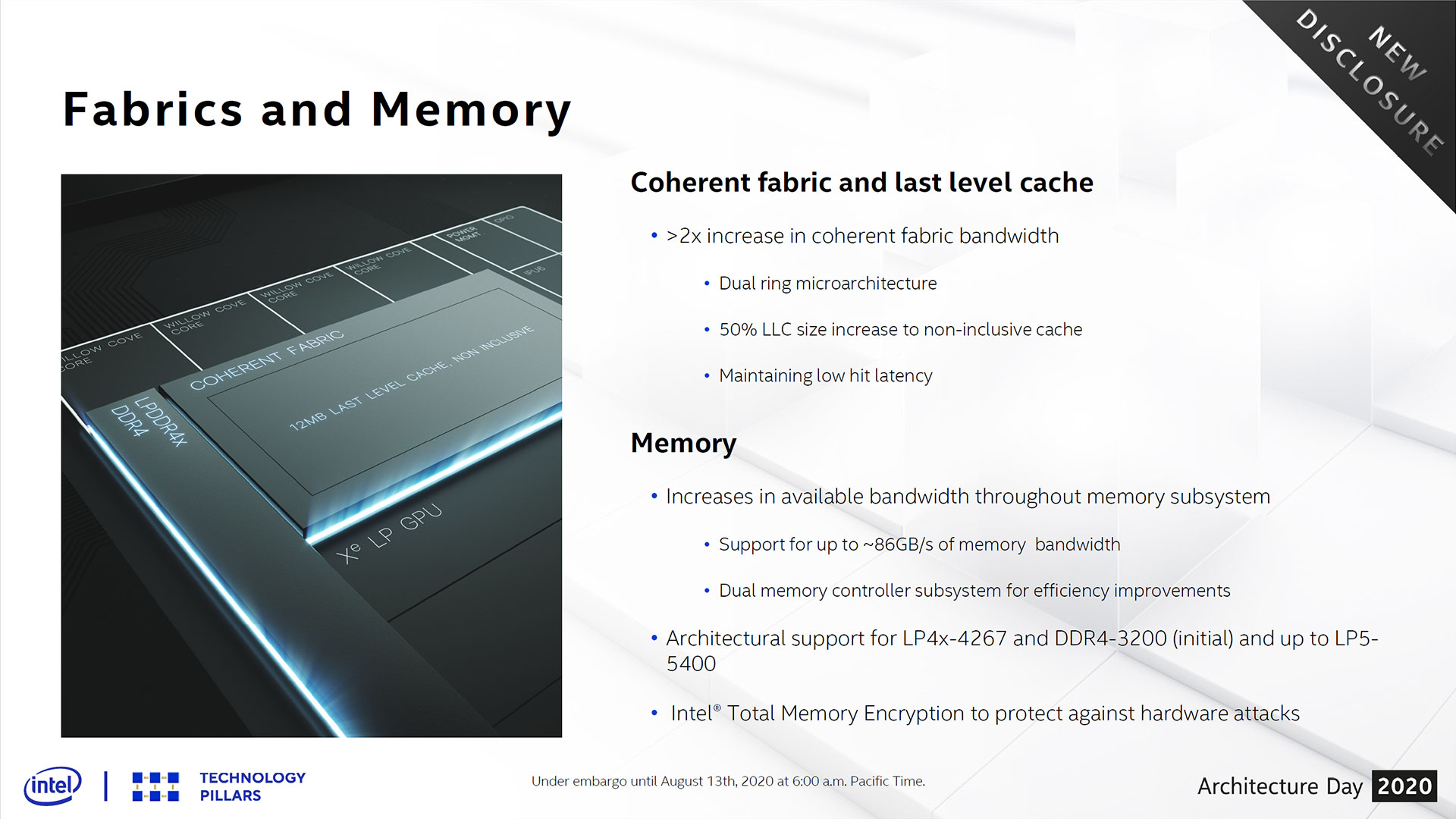

Intel has steadily changed its cache topology with its last few architectural upgrades, and yet another 'rebalancing' effort finds the company altering the Sunny Cove design as it moves to Willow Cove. Sunny Cove featured a somewhat drastic L1-D cache improvement from 32KB to 48 KB per core, along with a doubling of L2 cache to 512KB per core. However, Sunny Cove retained the same 2MB-per-core inclusive L3 cache scheme found on Skylake. Intel bumped that up by 50% to 4MB for Willow Cove and changed the cache from inclusive to non-inclusive. The larger L3 cache can hold more working sets to improve the cache hit ratio, but Intel hasn't elaborated on whether or not the larger non-inclusive cache will also contain all, or portions, of data stored in the L2 cache. The net effect is an increase to 12MB~24MB of L3 cache per chip, depending on the product (based on core counts).
Intel also beefed up the memory subsystem with deeper queues to improve scheduling efficiency and a second memory controller with support for DDR4-3200 and LPDDR4-4267 for now. However, the chipmaker made architectural provisions to support up to LPDDR5-5400 in the future. Sunny Cove has the same 128-bit memory bus width as Ice Lake, but Intel went from a 32b-wide quad-channel DDR4 controller to a 16b-wide octo-channel controller. The chip supports up to ~86 GB/s of memory bandwidth, a doubling over Ice Lake. That will certainly come in handy to feed the Xe LP Graphics engine.
With the move to more robust caches and faster memory, it's only natural that the on-chip fabrics have to improve in lockstep. Intel moved to the dual ring bus microarchitecture, though this varies significantly from the older dual ring busses found on high core-count Skylake-X dies of yore. Those dual ring busses served two distinct sets of cores with latency-incurring switches in-between to enable hops between the rings, with each stop on each ring only serving one core or element. In this design, each stop serves both bi-directional rings, meaning Willow Cove's dual ring bus is essentially two ring busses wrapped within one another. This approach doubles the coherent fabric's bandwidth, which is usually twice the memory bandwidth (172GB/s in this case). Interestingly, Intel has moved higher core-count chips to a mesh architecture due to its improved bandwidth, but chose to use a dual ring bus technique with Willow Cove.
Intel also sprinkled in a few new security features, like support for Total Memory Encryption (TME) using XTS/AES encryption/decryption algorithms to protect data held in memory. Control-Flow Enforcement Technology (CET) adds protection against some control-flow hijacking malware.
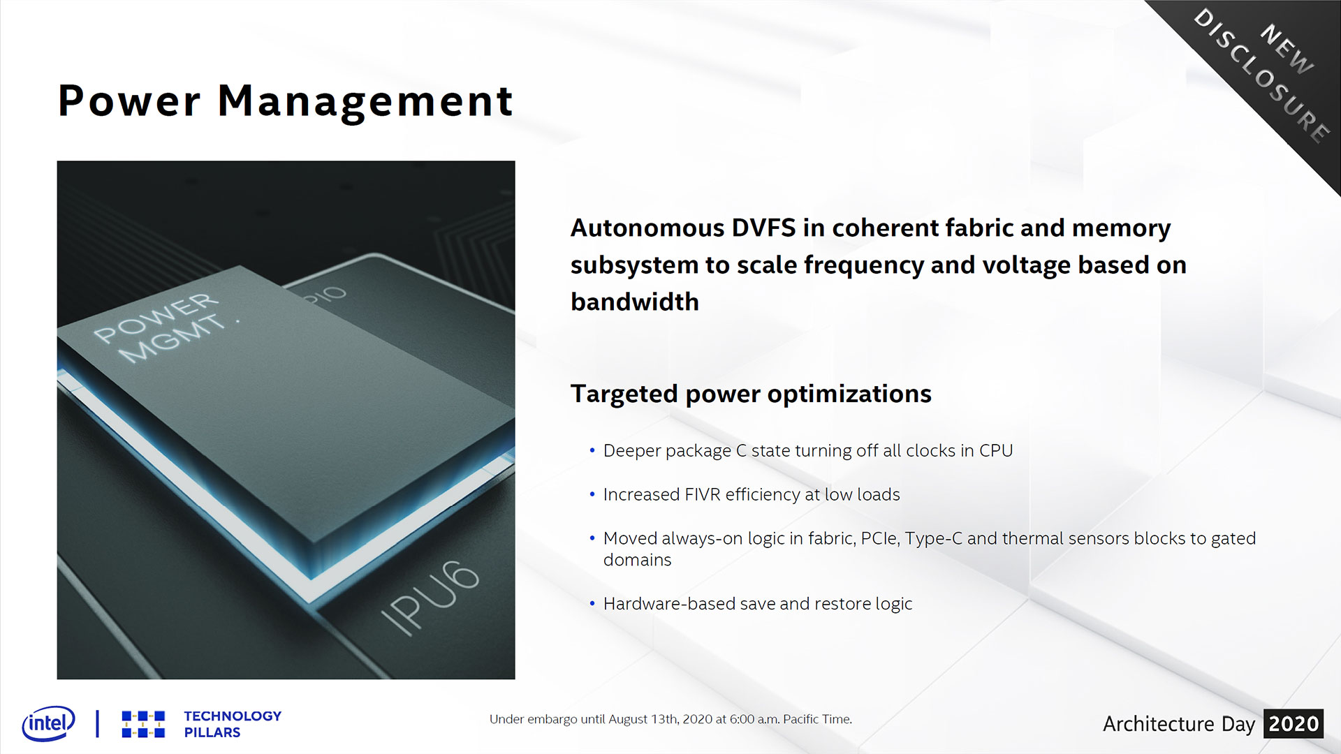
As part of the reworked memory and fabric subsystems, Intel also added in autonomous dynamic voltage/frequency scaling (DVFS) for the coherent fabric and memory subsystem, allowing them to modulate power consumption based upon usage. Other power enhancements include deeper package C-states that can turn off/reduce all the various clocks in the CPU, including newly power-gated subsystems like the fabric, PCIe, Type-C, and thermal sensors. Intel also lowered fixed rail voltages where possible and made unspecified changes to increase FIVR efficiency at lower load levels.
Intel reworked its High-vT devices, which are low-power low-performance transistors commonly used for I/O devices, like PCIe, Type-C interfaces, imaging, and the like. Intel made these devices more efficient by improving leakage, which then allows a lower operating voltage. That improvement also returns more power to the SoC for processing functions on either the CPU or GPU cores.
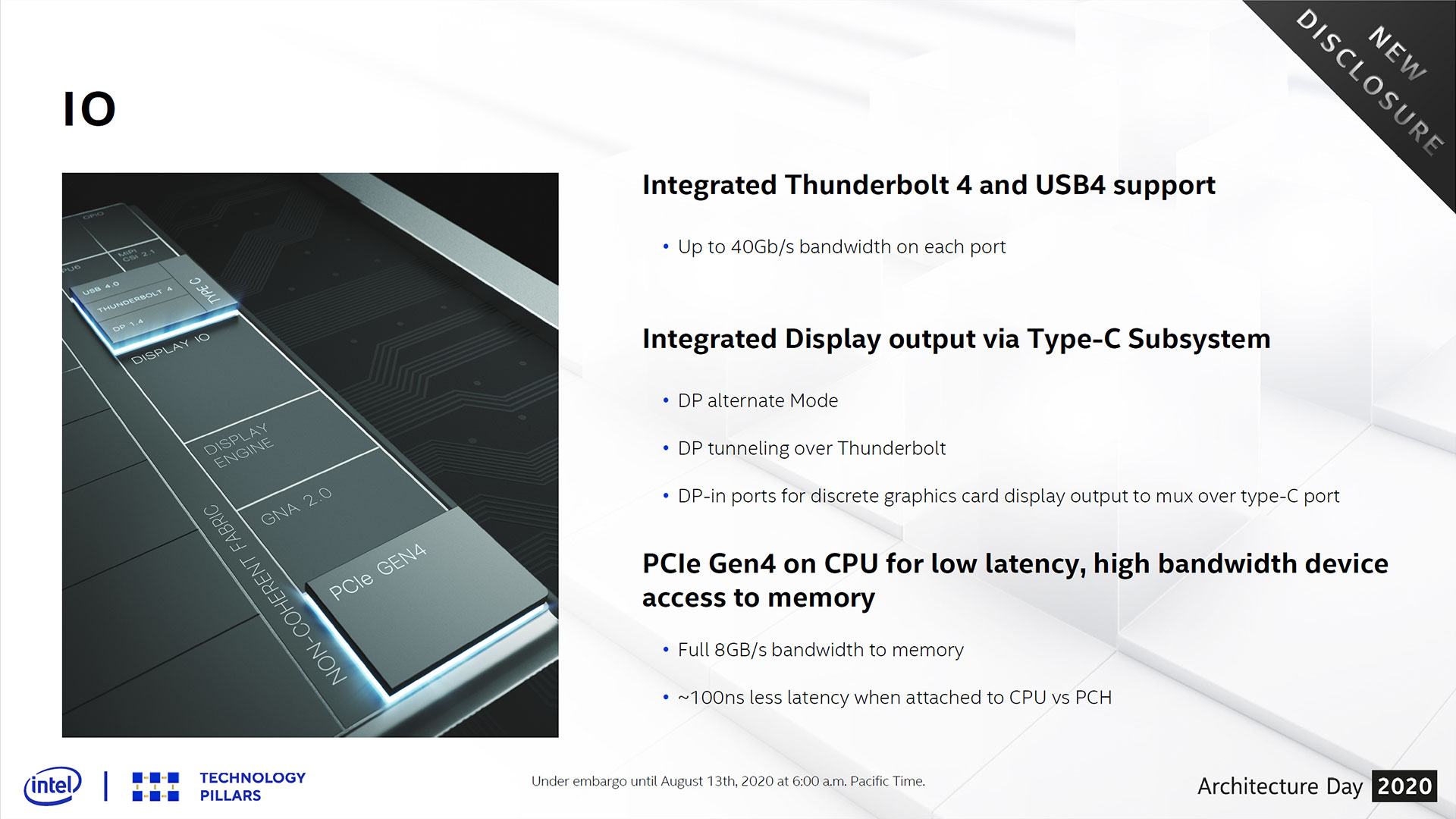
Unlike AMD's desktop Ryzen chips, the Ryzen 4000 "Renoir" Mobile APUs only support the PCIe 3.0 interface. That means that Intel finally has a connectivity advantage over Zen 2-based chips with its PCIe 4.0 connectivity in Tiger Lake, which offers twice the throughput of PCIe 3.0. Intel has also finally added support for a direct-attached PCIe storage device to the CPU. That means the chip features an unspecified number of lanes (varies by SKU) connected from the M.2 port directly to the CPU (the company says these lanes can also be used for GPUs).
In the past, Intel connected PCIe storage devices through the PCH, but it says the new direct-to-CPU PCIe 4.0 connection reduces storage latency by 100ns. Now, that sounds impressive if you measure in nanoseconds, but storage performance is measured in milliseconds. That means we're looking at a 0.00009ms improvement to latency, which is hardly meaningful. For reference, Intel's Optane SSD is the fastest SSD on the market (by far), and it has 0.014ms of latency. That means Intel's 100ns claim is meaningless in terms of storage performance (normal flash-based SSDs average between 0.1 and 0.06ms of latency).
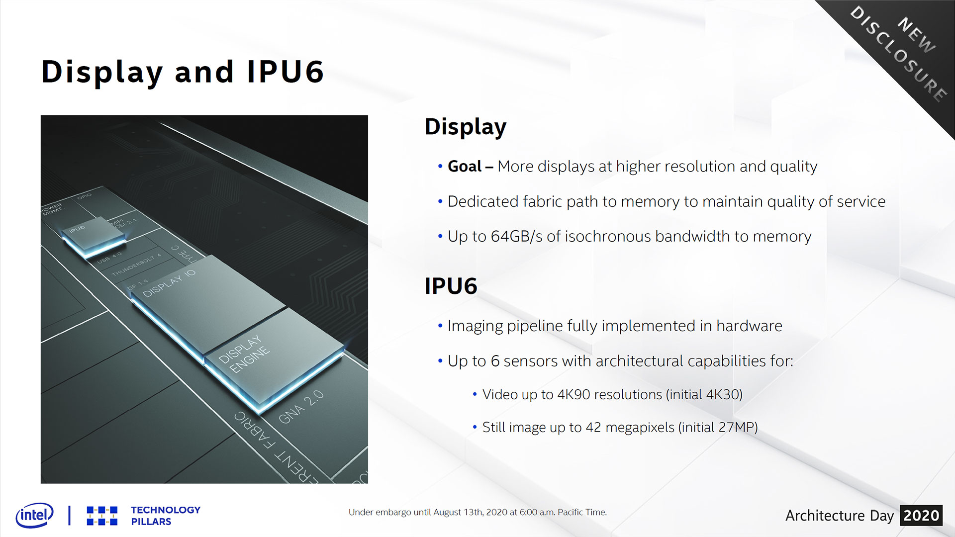
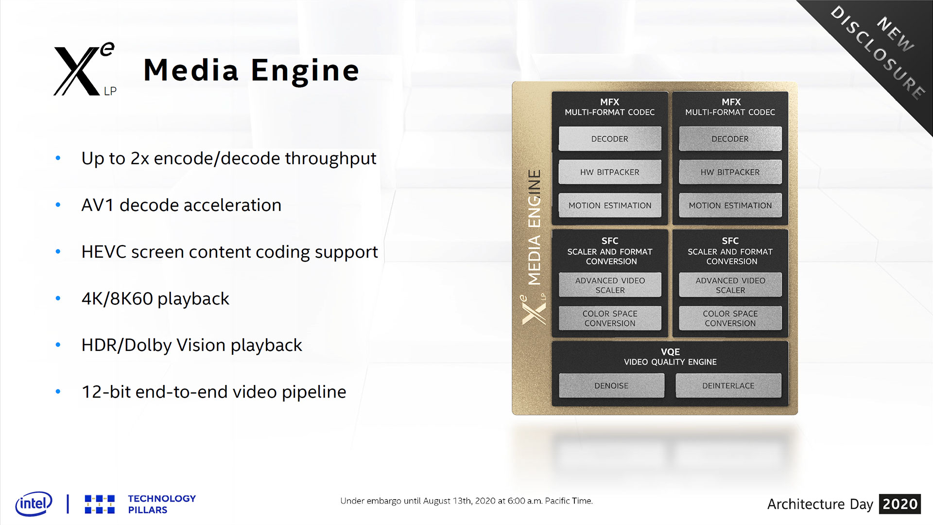
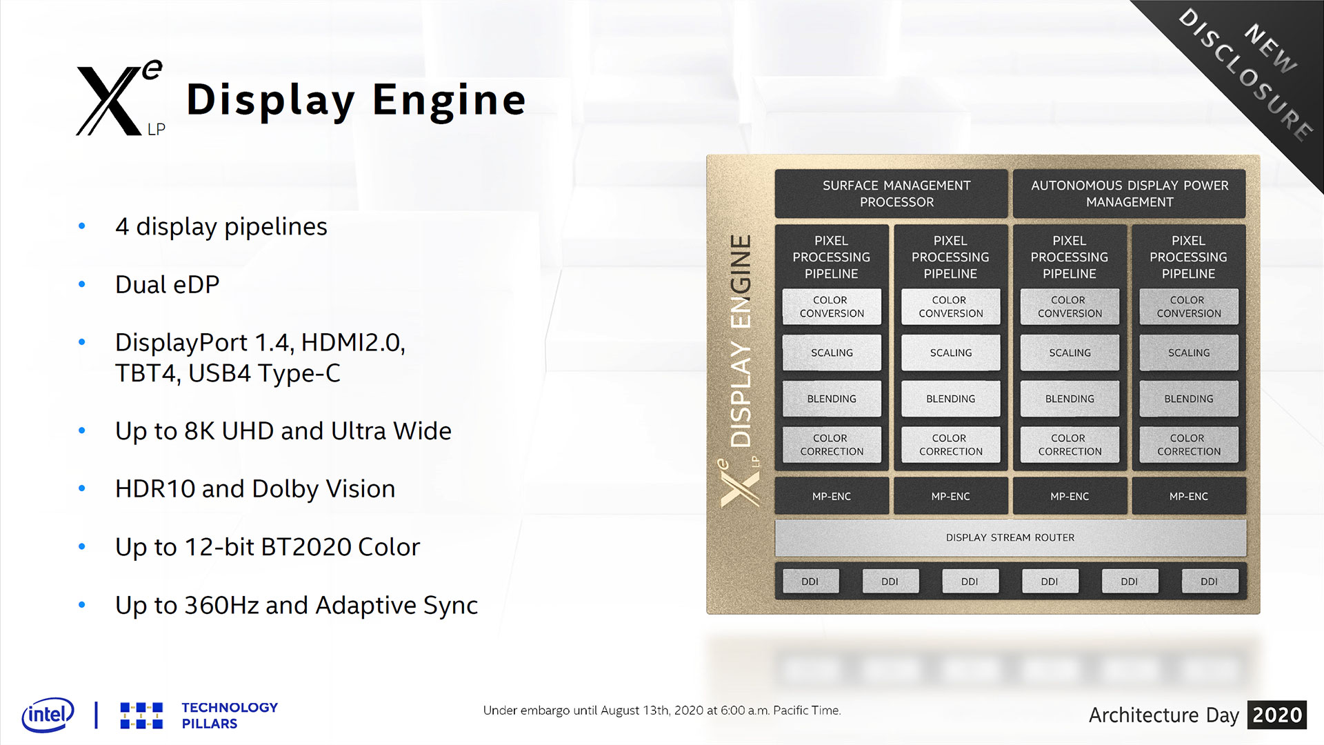
At least we get some meaningful improvements on the display side of the equation. Intel infused a 64-byte direct data path from the memory to the display so it can cut through the layers of arbitration in the chip fabric to ensure a solid QoS. That yields up to a 64GB/s isochronous low-latency pipe from the memory to the graphics, albeit with throughput varying by SKU. We're looking at support for AV1 decode, up to four display pipelines, 8K UHD and Ultra Wide, 12-bit BT2020 color, and 360Hz and Adaptive Sync, among others listed in the album above. Tiger Lake also supports up to six 4K90 sensors (support starts at 4K30) and can process still images up to 42 megapixels, an increase over the prior 27MP limitation with Ice Lake.
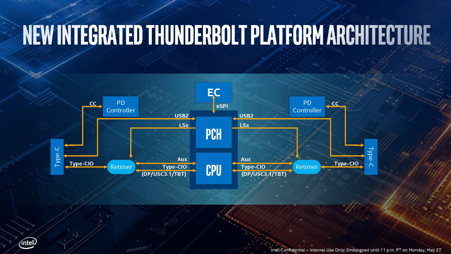
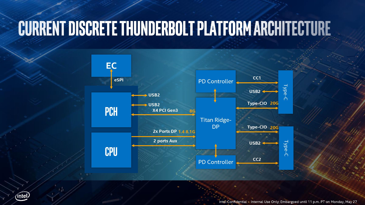
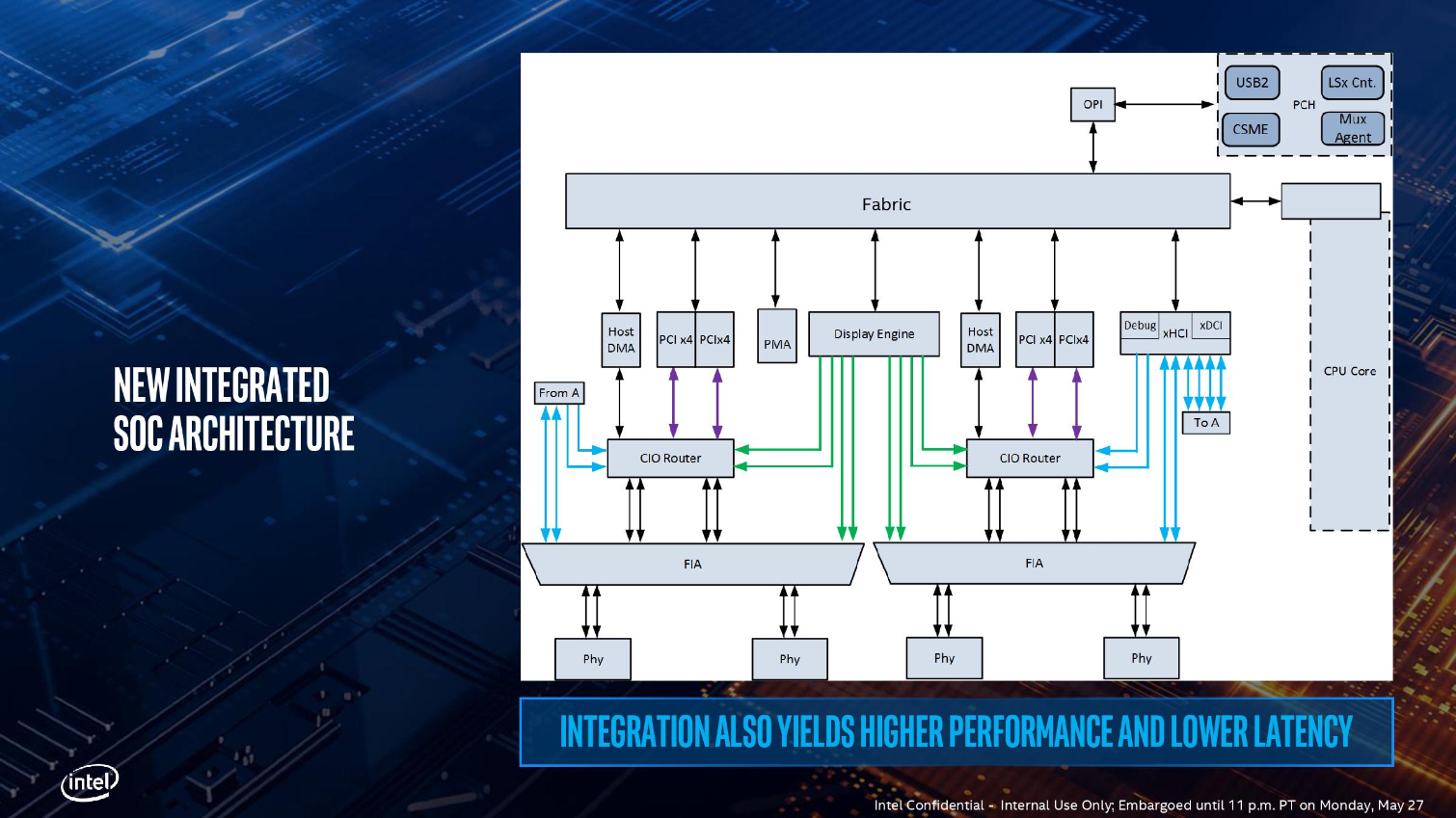
Intel touts its 'new' support for integrated Thunderbolt 4 and USB 4, but these aren't really 'new' protocols. In short, with speeds up to 40Gb/s, Thunderbolt 4 maintains the same maximum speed rating as its predecessor (TB3) and doesn't enable new features. Instead, in order to qualify for certification, vendors must enable all of the high-end features that used to be optional, like the ability to hit the 40Gb/s data throughput requirements and support two 4K displays or one 8K display. This approach does simplify the confusing branding surrounding Thunderbolt 3, but from a hardware standpoint, the speeds and feeds remain the same.
Intel designed a new dual-sided Thunderbolt 3 controller architecture for Ice Lake that provides up to 4 ports, two on each side of the laptop, with each port connected to a x4 PCIe 3.0 root complex on the chip. The integrated controller brought the features enabled by Titan Ridge, a secondary chip that enabled Thunderbolt 3 connections via connections to the CPU and PCH, onto the Ice Lake die. This implementation uses eight PCIe lanes operating at 20 GT/s, a reduction from the 17 lanes on Titan Ridge that ran at 8 GT/s, thus reducing the power consumption, complexity, and componentry associated with the Thunderbolt interface. Vendors still need to add re-timers and power control circuitry, but overall, this implementation significantly simplifies the design. Intel hasn't shared many fine-grained details on the new connection, but it will be interesting to see if the company leverages the faster PCIe 4.0 standard to reduce the lane count.
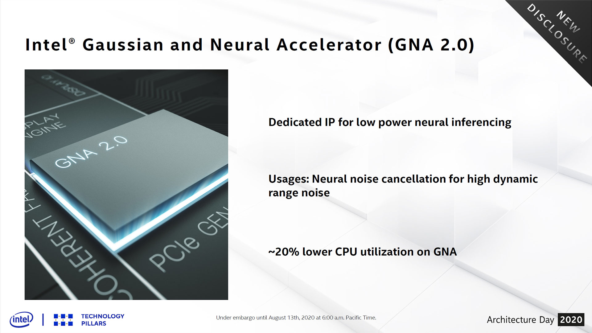
Intel carries over support for AI-boosting VNNI instructions (aka DL Boost - INT8/INT16) that leverage AVX-512 to boost the performance of convolutional neural networks. The Gaussian and Neural Accelerator (GNA) returns, but this time with a new 2.0 revision. This SoC-integrated AI accelerator block is used for processing all sorts of low-power voice-based applications, like translation and transcription, using low-power inferencing. Intel claims that this offload engine can reduce CPU utilization by 20% during these types of operations, but at a much lower power consumption of 1 gigaop-per-mW, with a max of 38 gigaops of performance.
That's Tiger Lake and Willow Cove in a nutshell, at least for now. Today's disclosures only cover the architectural bits of the design, so we still don't have a list of processors that will come to market, or their respective specs. We expect those details to come to light in the coming months as we move closer to launch, but the early signs look promising for Intel. Tiger Lake could serve to be a much-needed parry to AMD's Ryzen Mobile assault, which has found Intel's rival slowly chipping away market share in the mobility market. As always, the proof is in the silicon, and we can't wait for Tiger Lake to hit our labs.

Paul Alcorn is the Editor-in-Chief for Tom's Hardware US. He also writes news and reviews on CPUs, storage, and enterprise hardware.
-
Arbie So we'll have SuperFin transistors and Xe LP graphics in laptops by year end. OK; we'll see. That's a pretty concrete goal. As for all the 2021 and beyond stuff - it's amazing how little I trust Intel now, compared to years ago and compared to how reliable they should be.Reply -
JarredWaltonGPU Reply
I fully expect Tiger Lake laptops to launch on September 2. Pretty sure Intel has confirmed that. Yeah, it did:Arbie said:So we'll have SuperFin transistors and Xe LP graphics in laptops by year end. OK; we'll see. That's a pretty concrete goal. As for all the 2021 and beyond stuff - it's amazing how little I trust Intel now, compared to years ago and compared to how reliable they should be.
https://www.tomshardware.com/news/intel-tiger-lake-launch-event-on-september-2-xe-graphics
Xe HPG and dedicated GPU plans, I'm far less confident on when they'll arrive. -
spongiemaster Reply
Didn't the definitions of launch and available for sale diverge a long a time ago? Ampere looks like it is launching on the 1st, but everyone already knows you won't be able to buy one on that day. When will you be able to buy a TL laptop?JarredWaltonGPU said:I fully expect Tiger Lake laptops to launch on September 2. Pretty sure Intel has confirmed that. Yeah, it did:
https://www.tomshardware.com/news/intel-tiger-lake-launch-event-on-september-2-xe-graphics
Xe HPG and dedicated GPU plans, I'm far less confident on when they'll arrive. -
shawman123 I think we have already seen roadmap Tiger Lake laptops from all major OEMs. We should see laptops available starting next month. Even Ice lake laptops were available fairly quickly after launch. I am expecting cheaper brands like Inspiron, Pavillion, Ideapad available 1st and later we see premium brands like XPS, Spectre and Thinkpad.Reply
I am hoping to see premium brand like XPS/Surface etc come with LPDDR5. -
Giroro This all sounds pretty impressive. I wonder how Tiger Lake stacks up against AMD's 5nm Zen4 APUs, which will probably be its primary competitor by the time it actually gets released.Reply -
Giroro ReplyJarredWaltonGPU said:I fully expect Tiger Lake laptops to launch on September 2. Pretty sure Intel has confirmed that. Yeah, it did:
https://www.tomshardware.com/news/intel-tiger-lake-launch-event-on-september-2-xe-graphics
Xe HPG and dedicated GPU plans, I'm far less confident on when they'll arrive.
Intel confirmed a lot of different dates for 10nm over many years, and they still haven't fully brought that to market yet. -
shawman123 Tigerlake is already in production and there is a launch party(virtual) on 2nd September. Not just that we have seen laptops with TGL online from all major manufacturers. So you will not only see laptops next month but I am expecting to see them in Costco/Best Buy etc like Ice Lake laptops last year. Generally cheaper laptops launch initially for back to school before we see premium laptops.Reply
I had purchased an icelake laptop last November for $280. The deal said i3-1005G1 but people got i5-1035G4. Terrific deal considering RAM and SSD was up-gradable. I am sure we will see deals with TGL laptops this november as well(though not as crazy as icelake one last year). -
JarredWaltonGPU Reply
I'd disagree on that. Ice Lake has been readily shipping for over a year now. No desktop stuff yet, true. No server stuff either. 10nm clearly had some issues that were still being worked on until recently. But I expect to see quite a few new 10nm parts from Intel very shortly, spanning a wide range of applications. And I suspect Intel's current SuperFin 10nm (10nm++) will be pretty comparable on a lot of levels to TSMC / Samsung 7nm -- maybe better in some areas, maybe worse in others. Because really, TSMC and Samsung 10nm was more like Intel's 14nm++ (maybe one or two extra pluses).Giroro said:Intel confirmed a lot of different dates for 10nm over many years, and they still haven't fully brought that to market yet.
From everything that was revealed at architecture day, I also think Intel has reworked its 10nm plans quite a bit of late, basically knowing 7nm was also experiencing some problems and so 10nm will be around longer than originally planned. Well, not originally -- originally updated after 10nm tanked hard with Canon Lake plans. :-) -
watzupken Reply
Ice Lake processors have been in the market for some time, but it wasn't until this year before it became more widely available. Also as you mentioned, 10nm for other market segments are missing so far. So while I feel that Intel's 10nm have improved over the last 2 to 3 years, I suspect the yields are still poor. If not, they would not have cap Tiger Lake U to only 4 cores, and to date, I don't see any 10nm with more than 4 cores in the retail space. Even for desktop processors, they made the decision to backport Rocket Lake to 14nm instead of 10nm.JarredWaltonGPU said:I'd disagree on that. Ice Lake has been readily shipping for over a year now. No desktop stuff yet, true. No server stuff either. 10nm clearly had some issues that were still being worked on until recently. But I expect to see quite a few new 10nm parts from Intel very shortly, spanning a wide range of applications. And I suspect Intel's current SuperFin 10nm (10nm++) will be pretty comparable on a lot of levels to TSMC / Samsung 7nm -- maybe better in some areas, maybe worse in others. Because really, TSMC and Samsung 10nm was more like Intel's 14nm++ (maybe one or two extra pluses).
From everything that was revealed at architecture day, I also think Intel has reworked its 10nm plans quite a bit of late, basically knowing 7nm was also experiencing some problems and so 10nm will be around longer than originally planned. Well, not originally -- originally updated after 10nm tanked hard with Canon Lake plans. :)
As to how good Intel's 10nm is as compared to the likes of TSMC, that is hard to tell. Taking 14nm as an example, Intel's 14nm is definitely better than the other foundry. But with 10 and 7nm where Intel failed to delivery on schedule, they had to make compromises to make it work and appease both their investors and clients. This 10nm that they are using now is definitely not the same design that they have planned when they started exploring 10nm. -
TerryLaze Reply
It's not like TSMC process is great with them being limited to just above 4.2Ghz or something when all cores are running and needing heavy overclocks to reach 4.3 or 4.4 if you want to reach even the stock speed all core of intel ( 4.9Ghz for 10900k) on Ryzen you need liquid nitrogen.watzupken said:As to how good Intel's 10nm is as compared to the likes of TSMC, that is hard to tell.
It's great for low power portable/servers but desktop users need more umph otherwise people would only buy laptops.
