Intel Introduces New Mesh Architecture For Xeon And Skylake-X Processors
Intel's Akhilesh Kumar, the Skylake-SP CPU architect, penned a blog post today announcing the company's new on-chip mesh architecture for its Xeon Scalable Processor platform.
Intel's Scalable Processor platform is the company's re-branding of its venerable Xeon processor lineup, and due to the company's continued use of optimized server processor die for its HEDT (High-End Desktop) lineup for enthusiasts and workstations, the new architecture has wormed its way into the forthcoming Skylake-X family.
Intel's new mesh topology goes head-to-head with AMD's Infinity Fabric, which resides in its Ryzen, ThreadRipper, and EPYC processors. Let's compare the two designs.
Article continues belowThe Ring Bus Era
CPUs are all about processing data, which requires data movement. Bits representing 1s and 0s speed through the internals of the processor on nanometer-scale pathways that move on the order of billions of cycles per second. Moving data between the key elements, such as cores, memory, and I/O controllers, is one of the most daunting challenges involved with processor design.
Efficient data movement has a tremendous impact on performance, but all data movement also requires power for transit, so smooth and effective transmission is a key component to ensuring a low power envelope. This also helps constrain thermal output. Optimized interconnects, in turn, allow architects to dedicate more of the power budget to other useful pursuits, such as data processing. Several techniques have been employed over the years for intra-processor communication, but Intel's ring bus implementation has served as a cornerstone of the company's designs for the last several generations.
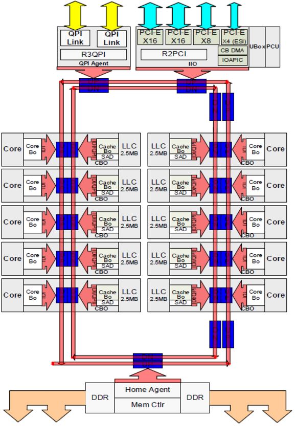
Intel's ring bus, shown above on the Broadwell LCC (Low Core Count) die, connects the various components with a bi-directional bus (in red). The LCC dies employ a single ring that propels data at a one-cycle-per-hop rate (among contiguous cores). For instance, moving data from one core to its closest neighbor requires one cycle. Moving data to more distant cores requires more cycles, thus increasing the latency associated with data transit. It can take up to 12 cycles to reach the most distant core, so the ability to move data in either direction (bi-directional) allows the processor to route it along the shortest path possible. Caches accompany each separate core on the die, so increased latency also impacts cache performance.
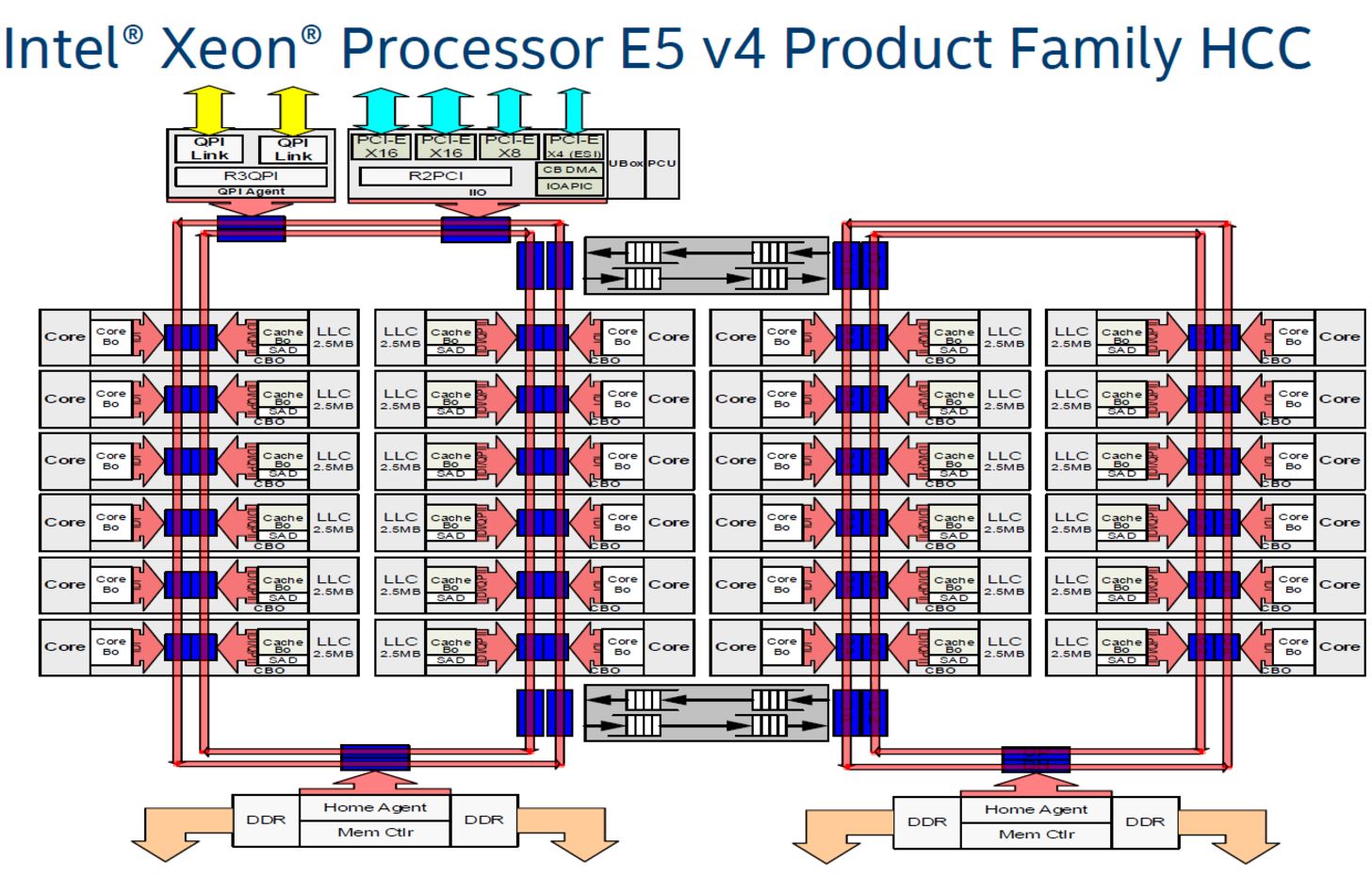
The larger HCC (High Core Count) die exposes one of the problems with this approach. To increase the cores and cache, the HCC die employs dual ring buses. Communication between the two rings has to flow through a buffered switch (seen between the two rings at the top and bottom). Traversing the switch imposes a five-cycle penalty, and that is before the data has to continue through more hops to its destination. This increased latency limits scalability. The intra-processor communication takes longer as core counts increase, impacting performance, and increasing the frequency to defray the performance loss requires higher voltage, thus impacting power consumption and thermal dynamics. Remember, processors can reach boost frequencies for longer periods of time based upon the internal thermal budget, so increased voltage can also negatively affect performance.
Get Tom's Hardware's best news and in-depth reviews, straight to your inbox.
Exposing The Mesh
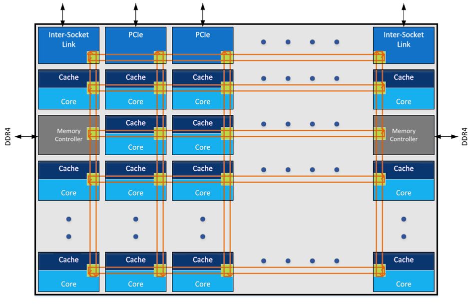
Intel's new mesh architecture made its debut on the company's Knights Landing products, but the move to the more mainstream server SKUs and high-end desktop models is designed to bring about new levels of interconnect efficiency for those markets. Aside from the interconnect, a few key attributes pop out. Intel has moved the DDR4 controllers to the left and the right sides of the die--similar to the Knights Landing design--whereas the company has typically positioned them at the bottom for ring bus designs. We'll examine that shortly.
Intel aligned its new mesh topology into a grid of rows and columns that connect the cores and caches, along with the memory and I/O controllers. Notably, there are no buffered switches between disparate rings--it's simply a large mesh, so it eliminates one of the major traffic checkpoints for high core count dies entirely. The switch connections at each intersection of the grid allow for more direct communication between the components, thus providing faster pathways through intelligent scheduling. There also appears to be a circular design to the intersections, which likely allows for more optimized data path scheduling.
The ability to 'stair-step' data through the cores allows for much more complex, but efficient, routing among the elements. Intel also indicates that the new ring has increased bandwidth, which helps speed data traffic among the cores and the caches that feed them. The mesh is also responsible for traffic to and from main memory, so it has an impact on RAM throughput and latency as well.
Data also flows in from the PCIe controllers at the top of the die, along with the two inter-socket links. The inter-socket links manage data flow between processors in 2+ socket server configurations. In the past, Intel has employed its QPI (QuickPath Interconnect) for cross-socket communication, but it's rumored to employ a new UPI interconnect for Skylake server CPUs (Purley). Intel hasn't specified the exact frequency of the new mesh, but has indicated that it has a lower frequency and voltage than the ring bus design, though it still delivers high bandwidth and low latency. That alone is an important achievement.
The modular and distributed design should allow Intel to add more cores to its die without imposing crushing performance and power consumption penalties. The mesh design also reduces latency variability when requesting data from far-flung LLC banks, which allows software to treat it as one large unified last-level cache.
So What About Skylake-X?
Intel released a die shot of its HCC (High Core Count) die that it employs for the Skylake-X processors. Again, Intel uses the same architecture for its Xeon lineup and for the enthusiast-class parts, so Skylake-X employs the same mesh interconnect topology.
We can clearly see the relocated DDR4 controllers on the right and left of the die (second row down on both sides), so while it appears the die has 20 cores, it 'only' features 18. This happens to be the maximum core count of Intel's new Skylake-X lineup.
Intel's mesh diagram indicates that it aligns the mesh intersections at the right side of each core, but the die shot implies otherwise. If we examine the cores on the far left column, we can see a distinct area of the core in the upper right corners, which the block diagram implies is the rough location of the interconnect. However, examining the adjacent column of cores indicates that the cores are mirror images of each other. This implies that instead of the mesh pathways running along the right side of each core, they might run on the left side of each mirrored column. This would have an impact on the distance between every other column of cores, which would translate as more cycles required for horizontal data traversal. For instance, it likely requires one hop/cycle to move data vertically to the next core, but moving horizontally from the second column to the third column will likely require more cycles. We'll have to wait for more detail.
In either case, the mesh architecture has a tremendous scalability advantage over its predecessor, and considering that Intel used the ring bus for several generations, we can expect the company to use the mesh for the foreseeable future. That should allow Intel to increase core counts without adverse performance penalties.
So What's AMD Up To?
No conversation about an Intel architecture is complete without a comparison to AMD's latest design. AMD also developed a new Infinity Fabric interconnect, which is an optimized version of HyperTransport, for its Zen microarchitecture. Fortunately, we know much more about AMD's interconnect.
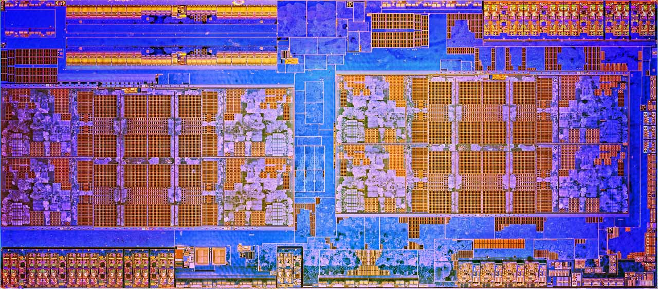
AMD's Zen-based processors take a different path to processor design. The Zen microarchitecture employs a four-core CCX (CPU Complex) building block. AMD adorns each CCX with a 16-way associative 8MB L3 cache split into four slices; each core in the CCX accesses this L3 with the same average latency. Two CCXes come together to create an eight-core Ryzen 7 die (the large orange blocks in the image above), and they communicate via AMD’s Infinity Fabric interconnect. The CCXes share the same memory controller. This is basically two quad-core CPUs talking to each other over the Infinity Fabric pathway. The Infinity Fabric is a 256-bit bi-directional crossbar that also handles northbridge and PCIe traffic.
Although each core in a four-core CCX can access the local cache with the same average latency, trips to fetch data in adjacent CCXes incurs a latency penalty due to the trip across the Infinity Fabric. Communication between threads on cores located in disparate CCXes also suffers. AMD's design held a scalability advantage over Intel's ring bus architecture -- the company can simply infuse more CCXes onto the package to increase the core count. In fact, the 16C/32T ThreadRipper processors employ four CCXes. Due to the latency penalty for cross-CCX traffic, this could result in variability for some traffic. We expect the Intel marketing machine to push the new mesh architecture as an advantage over the Infinity Fabric, but it's notable that software optimization can defray many of the penalties associated with the Infinity Fabric.
We measured AMD's Infinity Fabric latency in our AMD Ryzen 5 1600X CPU Review and found that the speed of the fabric is tied to memory frequency, so faster memory data rates results in lower latency. This has a significant impact on Ryzen's gaming performance. We also measured Intel's ring bus latency with faster memory frequencies but found that it remains largely unaffected. It will certainly be interesting to test latency with the Skylake-X products to determine if the new mesh has distinctive characteristics.
The Wars Rage On
The return of a competitive CPU market has both Intel and AMD touting their latest architectural advantages, and both the mesh and AMD's Infinity Fabric will likely power the respective company's designs for the next several product generations, albeit with optimizations along the way. For instance, Intel's ring bus debuted back with Nehalem in 2007, and AMD's HyperTransport also served as an interconnect architecture that spanned multiple products.
Each architecture will have its strengths and weaknesses, and the only way to quantify performance advantages is to test the silicon. We're eager to get our hands on the new Skylake-X models to see if the new mesh topology offers tangible performance benefits. Stay tuned.

Paul Alcorn is the Editor-in-Chief for Tom's Hardware US. He also writes news and reviews on CPUs, storage, and enterprise hardware.
-
compprob237 Nice article. I was curious about the Mesh but never looked in to it. Looks like AMD bringing the competition has brought about innovation from the stagnant Intel.Reply -
JamesSneed Interesting, hope to see some reviews on Monday. I'm pretty curious how the 7820x will turn out.Reply -
Dugimodo Competition is good, but intel haven't just plucked this design out of the air in response to AMD releasing Ryzen. The truth is if all intel wanted to do was compete with Ryzen they already have products that match or better them and all they'd need to do is drop the prices - admittedly hugely. I'm impressed by Ryzen, but it only wins on price.Reply -
JamesSneed Reply19821430 said:Competition is good, but intel haven't just plucked this design out of the air in response to AMD releasing Ryzen. The truth is if all intel wanted to do was compete with Ryzen they already have products that match or better them and all they'd need to do is drop the prices - admittedly hugely. I'm impressed by Ryzen, but it only wins on price.
I have to disagree a bit. If you compare Ryzen to the fastest non HEDT CPU, the 7700k, there are lot workstation and scientific tasks Ryzen is faster than Intel. Threadriper is coming to compete in the HEDT line so I think we can have more apples to apples discussions instead of comparing Ryzen to Intel's HEDT line which is a bit disingenuous. Will your statement hold true once all the chips on the table, maybe, but I think before we jump to conclusions we see Intels and AMD's HEDT chips then call it.
-
Rookie_MIB Reply19821430 said:Competition is good, but intel haven't just plucked this design out of the air in response to AMD releasing Ryzen. The truth is if all intel wanted to do was compete with Ryzen they already have products that match or better them and all they'd need to do is drop the prices - admittedly hugely. I'm impressed by Ryzen, but it only wins on price.
Well, if you factor in price AND performance, then it comes out ahead. Yes, in raw speed Intel has faster cores, but you pay through the nose for those faster cores. For everyone else except the independently wealthy or large enterprise customers, they need the best bang for their buck - and that's what Ryzen provides.
(disclosure - I have a Ryzen 1700 - and boy it has some processing power)
-
ClusT3R Lol like always AMD innovating and the other has been the copy cat, the funny thing here they were force to change the architecture I don't know ho much but now if when you are going to see APPs that needs to bee optimize for that thing and is when people are going to understand what the innovations process cost to AMD all this years.Reply -
bit_user After seeing this on Xeon Phi v2 (KNL), I was wondering whether we'd see it in E5/E7 Xeons. Rings only get you so far.Reply
BTW,
trips to fetch data in adjacent CCXes incurs a latency penalty due to the trip across the Infinity Fabric. Communication between threads on cores located in disparate CCXes also suffers.
This is redundant. Threads communicate via caches & memory. -
homeles The "mesh" thing has been in the works for ages. David Kanter over at Realworldtech predicted that Skylake-EX would use it back in January 2014. The TeraScale project was Intel's first (at least publicly) exploration of a 2D mesh, and that presentation was back at ISSCC 2007. Knight's Landing already uses it. It has zero to do with AMD.Reply
Now is Intel making changes in response to AMD? Surely they are. Where you'll see this is with marketing, SKUs, and pricing -- you can change this on the fly. Something like this "2D mesh" however has been in the works for over a decade, and to claim that "it must be AMD!" is perhaps the single most asinine claim I have read in my entire time of following hardware (a good 7 years or so).
- III-V -
kinggremlin Reply19821616 said:Lol like always AMD innovating and the other has been the copy cat, the funny thing here they were force to change the architecture I don't know ho much but now if when you are going to see APPs that needs to bee optimize for that thing and is when people are going to understand what the innovations process cost to AMD all this years.
Intel demonstrated a 48 core cpu that utilized a mesh topology back in 2009, LONG before AMD was talking about infinity fabric. Intel didn't just magically come up with this in an instance in response to AMD. -
InvalidError Reply
Intel didn't put Skylake-X together overnight. For its mesh arrangement to be about to hit production silicon now, Intel must have made the design decision somewhere in the neighborhood of two years ago.19821616 said:Lol like always AMD innovating and the other has been the copy cat, the funny thing here they were force to change the architecture
Also, that's the third time Intel has changed its server CPUs' internal interconnect arrangement despite its monopoly position in the server space and this newest scheme bears a striking resemblance to Altera's FPGA scheme where extra D-flops are buried in the routing fabric, so I strongly suspect that the new routing arrangement is closely related to Intel's acquisition of Altera a few years ago - buy a programmable logic chip company, integrate some programmable logic related architecture in new CPUs.
Additionally, although Intel may have been slacking off in the low(er) margin mainstream and HEDT markets, its higher-end server CPUs have continued scaling as Intel needs more powerful and power-efficient chips to get repeat sales from companies that have already bought their previous-gen chips at those crazy E5/E7 prices and profit margins.
AMD's Ryzen/TR/EPYC have nothing to do with it, that's where Intel was going on the server side regardless.


