Skylake Xeon Platforms Spotted, Purley Makes A Quiet Splash At Computex
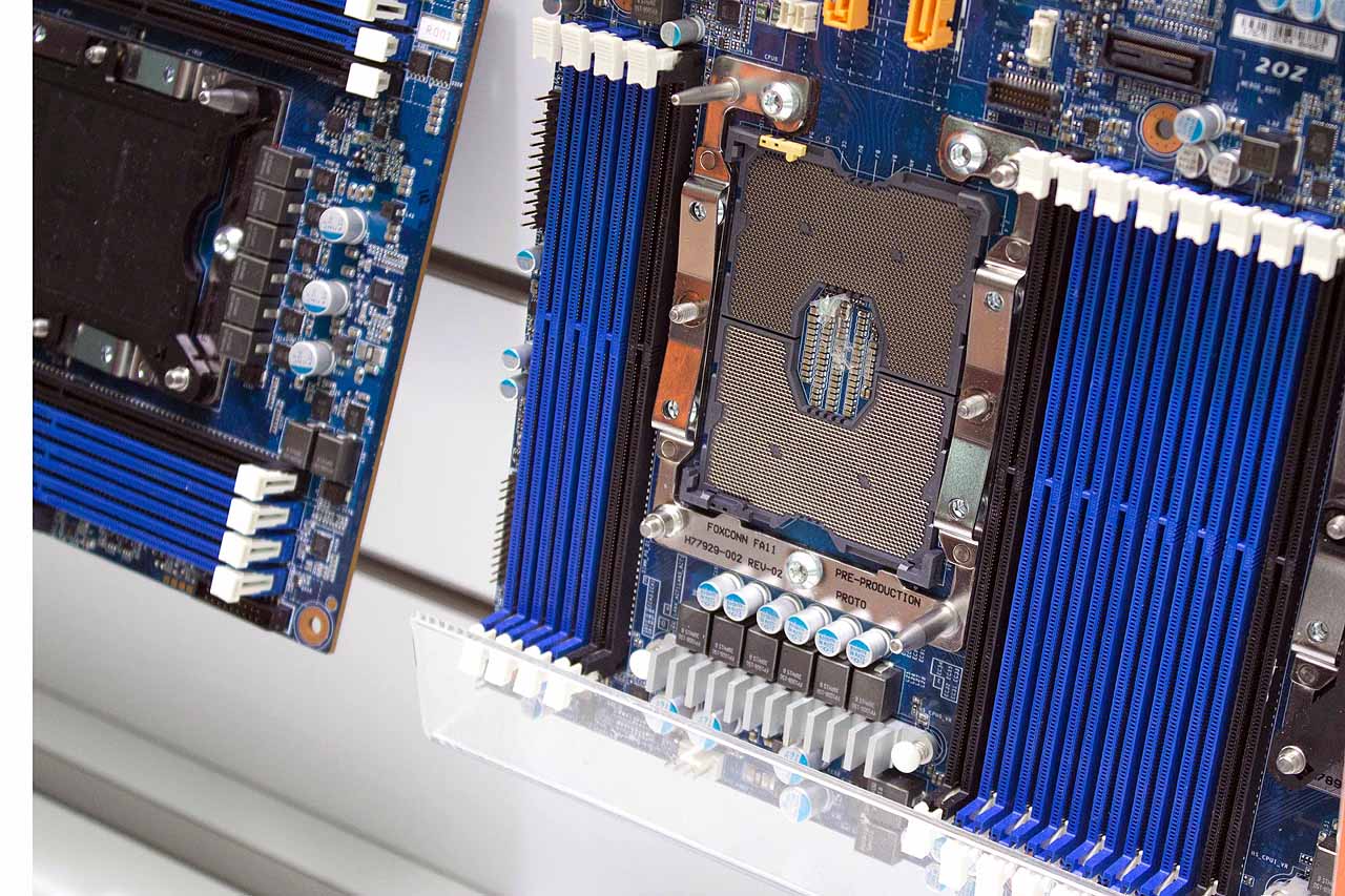
Intel's forthcoming 14nm Skylake Xeons are still in development, but a motherboard vendor here at Computex 2016 already had several Purley platforms (which will house the new chips) on display in its suite. Intel has not publicly shared any information on the new platform, but the boards indicate that the company has working silicon and is on the downward side of development.
Intel purchased Altera for $16.7 billion in December 2015 to gain access to FPGA (Field-Programmable Gate Array) technology. FPGAs (as the name implies) can be reprogrammed in the field to boost performance for specific tasks. Intel has publicly stated that it will incorporate FPGAs on-die with the current generation of Xeons, and there is no doubt that this practice will continue with the Purley platform. The next-generation Xeons will apparently be larger affair, which indicates that Intel engineered in plenty of room for FPGAs and GPU accelerators.
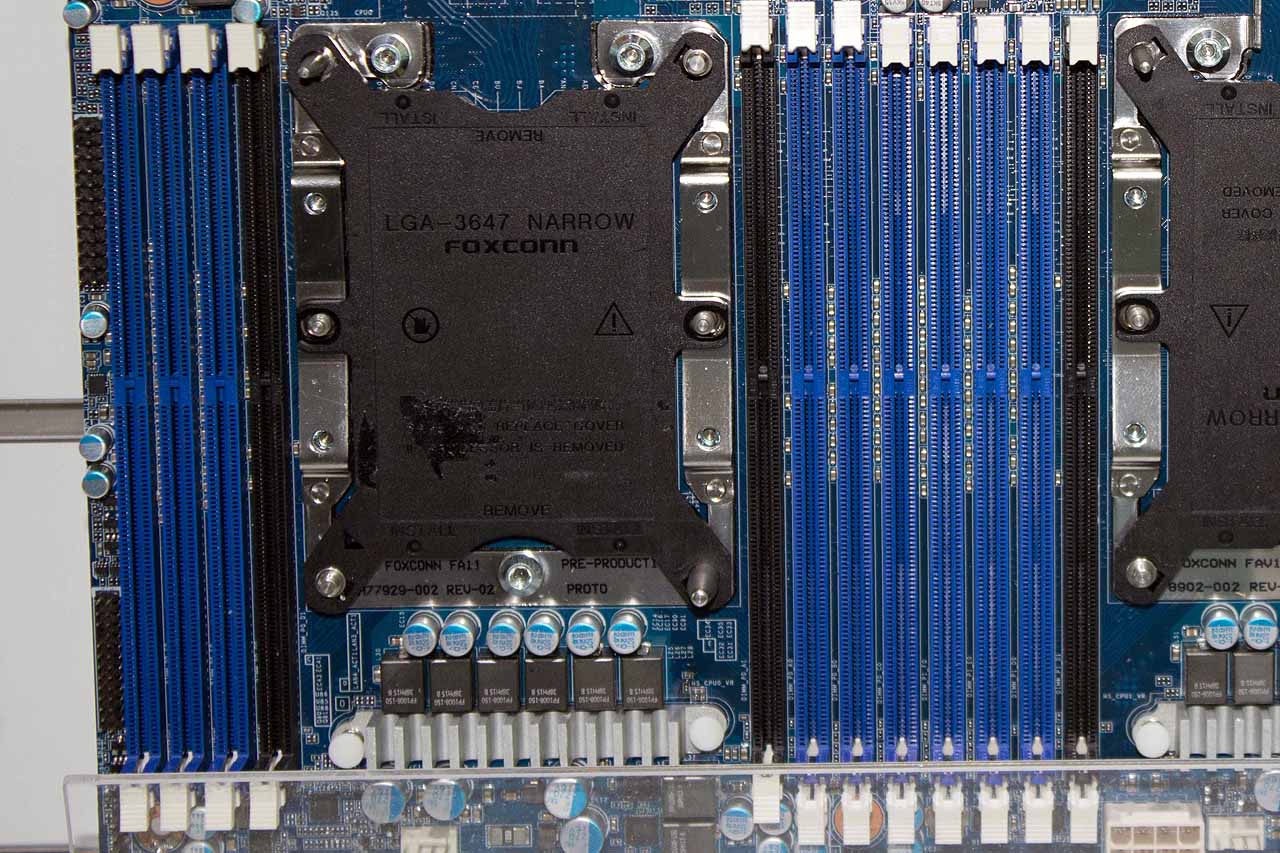
We did not have a ruler handy to measure the socket, but the JEDEC-compliant DDR4 slots that flank the socket are of the normal size, thus illuminating the mammoth nature of the next generation Xeons. The socket cover indicates that it is an LGA 3647 socket, meaning it packs in an additional 1,636 pins in comparison to the LGA 2011 socket (likely needed for additional paths into the aforementioned FPGAs).
Article continues belowA dual-socketed sled was also on display, and we note that the narrow ILM socket arrangement is present on both boards. The large rectangular socket would likely consume a considerable amount of motherboard real estate with a normal square ILM configuration.
There are precious few Intel-provided details on the new architecture, but a widely circulated document was discovered on a website owned by Konferencji Uzytkownikow KDM (the HPC User Conference). Marcin Kaczmarski, the Senior Sales Manager for central and Eastern Europe (at the time), purportedly presented the PDF at an HPC conference. A picture with Kaczmarki at a conference in front of one of the slides appears to lend some credence to the documents. However, as we were not there physically to confirm the details, we caution readers that the following technical details traipse into unconfirmed territory.
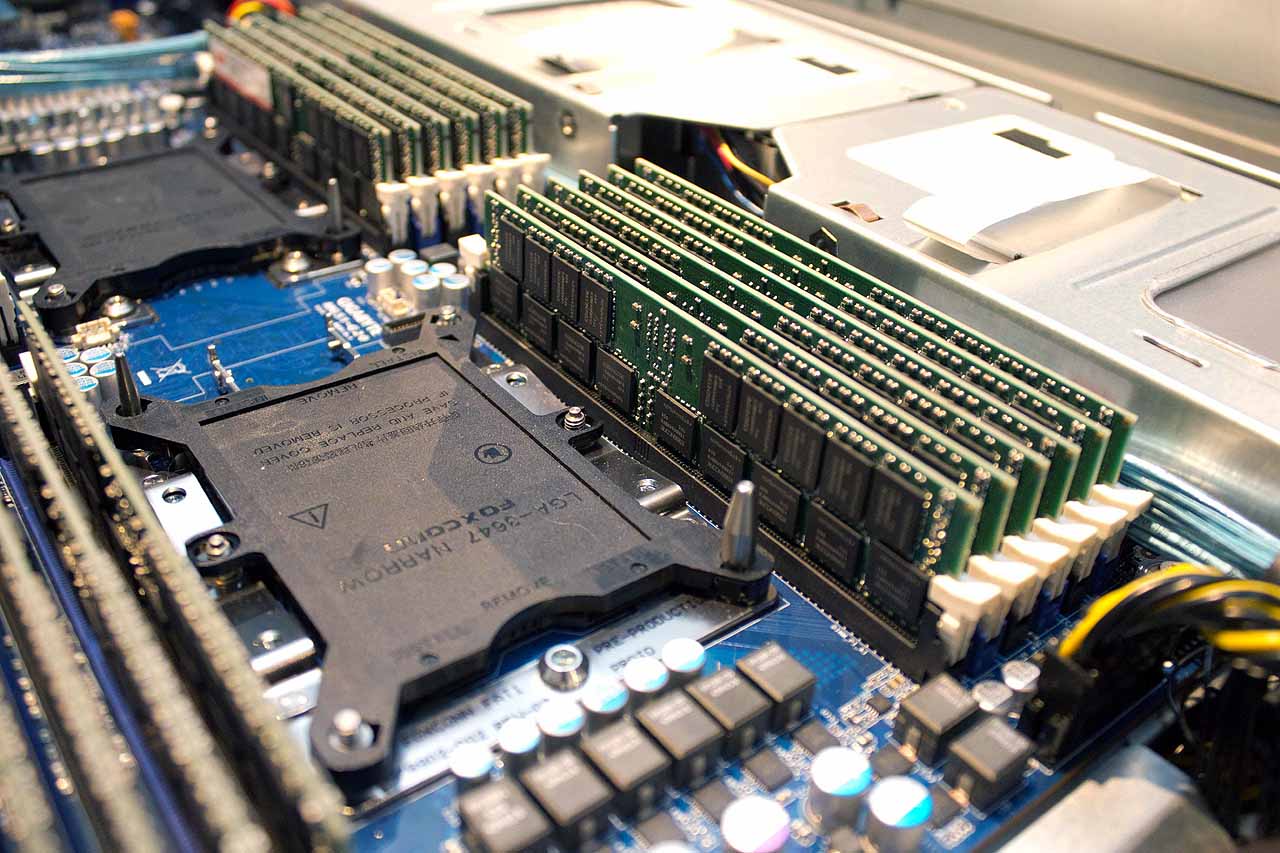
The incredible size of the processors begs the TDP question, as dense designs are particularly TDP-sensitive. The slides indicate that the Purley platform features a configurable TDP that ranges from 45 to 165W, and as the 2U system on display confirms, this can be dissipated in a dense configuration. The documents indicate that the 28-core/56-thread Purley platform will feature an on-die Intel Omni-Path architecture (a 100 Gbps fabric for HPC applications), along with the requisite 1 and 10 GbE connectivity options.
The slides also tout a persistent "all new memory architecture" that offers up to 4x the capacity of RAM and 500x the performance of NAND. These specifications do not align exactly with Intel's much-ballyhooed 3D XPoint claims of "1000x the performance and endurance of NAND with 10x the density of DRAM." The Purley presentation reportedly occurred on May 11, 2015, which is before the official 3D XPoint announcement on July 28, 2015. This suggests that Intel may have tweaked the final performance specifications between the presentation and the formal announcement.
Get Tom's Hardware's best news and in-depth reviews, straight to your inbox.
The 2U server we observed at Computex features a total of 12 memory slots per socket, which is indicative of a new hexa-channel memory controller. This tracks well with other industry reports at Computex that Intel is laying the 3D XPoint foundation by enabling more slots for system memory on emerging platforms, such as Kaby Lake. We expect 3D XPoint-based NVDIMMs will play a large role in the Purley platform, as well.
The platform will support both E5 and E7 processors and scale to 2, 4 and 8-socket implementations. The slides indicate the new platform will offer up to 1.5x the memory bandwidth and utilize new AVX-512 instructions, along with optional QuickAssist and Cannonlake graphics and media transcode accelerators. There is also the notable mention of a new 2- and 3-channel UPI interconnect that supports 9.6 and 10.4 GT/s data transfers. The UPI acronym is undefined at this point, but many speculate that it will serve as a faster and more scalable replacement for the QPI interconnect.
All conjecture aside, the presence of Purley systems at Computex 2016 indicates that we are rapidly approaching a new platform launch. The new platform will be faster than the previous generation, but that is to be expected. The real news is that Intel is embracing FPGAs to counter the death of Moore's law.
Intel will likely deploy FPGAs, and other accelerators, on an as-needed basis for large custom orders, so it may be a modular architecture. There might be standard SKUs with FPGAs, as well. We are likely more than a year away from an enthusiast-targeted Purley implementation, and frankly, it would be hard to imagine it including FPGAs. In either case, it will certainly be interesting to see what Intel has in store.
Paul Alcorn is a Contributing Editor for Tom's Hardware, covering Storage. Follow him on Twitter and Google+.
Follow us @tomshardware, on Facebook and on Google+.

Paul Alcorn is the Editor-in-Chief for Tom's Hardware US. He also writes news and reviews on CPUs, storage, and enterprise hardware.
-
therealduckofdeath ReplyWow, those sockets are colossal. I've never seen a socket that big in my life.
Yeah that looks yuuuge! I guess that's the price to pay for maximizing memory bandwidth. A lot of memory lanes means a lot of pins. :D
-
gangrel Can't be for just memory, not THAT many. 64, maybe 128, OK, but this is crazy many pins. It's 500 more pins than you would need to do some weird socket 2011 + socket 1151 configuration.Reply
I wonder if the pins are mostly to support interconnections between sections of the FPGA...for parallel processing support, for example...and/or with the rest of the processor -
therealduckofdeath It's got a quad channel memory controller, (rumour has it that future processors might have 6 memory channels; that's 384 pins just for the data), add a few for address and other selector bits. Add a 40 lane PCI bus. That requires a lot of pins. The motherboard interconnects wouldn't plug straight into the processor.Reply -
bit_user Reply
This is the future platform with 6-channel memory. Maybe the first board shown only supports 4, but the board in the second & third pics has 6 DIMMs on each side of both CPUs.18065537 said:It's got a quad channel memory controller, (rumour has it that future processors might have 6 memory channels;
It's tempting to speculate about the black DIMM slots, in the first pic - that they might be only for NVDIMMS, or something. In that case, I don't know why they'd be closest to the CPU, though. Maybe they just go in normal DIMM slots, and this is why Intel went to 6-channel.
Anyway, don't forget about OmniPath. Surely, they'll need some pins for that!
-
bit_user ReplyThe incredible size of the processors begs the TDP question
This is mis-formulated. Begging the question is where the answer to the question is included in its phrasing. And even though a large socket suggests a high TDP, I wouldn't say it begs the question. -
gangrel Well, ok...but expanding from 256 to 384 pins for memory access, only adds 128 pins, and that's not even related to the FPGA functionality, really. You'll do this any time you push to 6 memory slots. Going to 12 slots might blow things up to 768 for data; not sure how many for control. This slot has *1600* more pins. :)Reply -
bit_user ReplyThe real news is that Intel is embracing FPGAs to counter the death of Moore's law.
It might have more to do with customers like Google wanting to accelerate things like machine learning in hardware. Perhaps it's a hedge against Xeon Phi's successor (Knight's Landing) failing to compete with GPUs. Or maybe OEMs just demanded it, as a way to further differentiate their product offerings.
I think it'd be interesting to know whether Xeon D basically freed them from having to worry about the single-CPU use case. So, they could basically focus Purely on scalability. -
bit_user Reply
I'm puzzled by what pins people think would be added for FPGA. Why wouldn't it just sit on PCIe or the internal bus connecting the cores?18065784 said:that's not even related to the FPGA functionality, really. You'll do this any time you push to 6 memory slots. Going to 12 slots might blow things up to 768 for data
And the slides we've seen indicate this is only 6-channel - not 12. There can be multiple DIMMs per channel, which is especially common in servers (which use registered memory, with its lower electrical load, specifically for this purpose).


