Intel/Micron Introduces Revolutionary 3D XPoint Technology: Memory And Storage Combined
Get Tom's Hardware's best news and in-depth reviews, straight to your inbox.
You are now subscribed
Your newsletter sign-up was successful
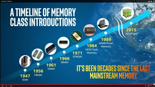
NAND, the last new storage-class memory, was introduced more than 25 years ago. We haven't seen a new form of memory to address the DRAM segment since 1966. That changed today, as Intel and Micron introduced the new jointly-developed 3D XPoint memory technology. Intel and Micron have over a decade of experience working together in the NAND field through their IMFT (Intel Micron Flash Technologies) venture, and have been working on developing 3D XPoint since the inception of their relationship.
The pace of innovation in the computer industry is legendary; the speed of the CPU has increased 3,500x, and it is 90,000x more efficient and costs 60,000 times less than it did when the first Intel microprocessor debuted in 1971. Memory, on the other hand, has lagged painfully behind. Storage has been increasingly picking up steam through the development of NAND flash memory, but even the fastest NVMe PCIe SSDs on the market lag behind, 10,000 times slower than today's CPU's.
There were some early signs that Intel and Micron were going to shake up both the memory and storage market when Intel introduced commands for persistent memory, CLWB and PCOMMIT, last November. This set off a furious round of speculation in the analyst community that something big was in the works.
Article continues below3D XPoint addresses all of the key requirements to address the gap between CPU speed and memory with 1000x faster performance and 1000x more endurance than NAND, and 10x the density of DRAM, and the icing on the cake is that this new technology is non-volatile.
Non-volatile characteristics are extremely important to bridge the gap between DRAM and NAND. "Non-volatility" simply means that the new memory medium retains data without power. Bringing this capability to a device that is exponentially faster than NAND enables capabilities well beyond any other form of memory.
We measure HDD latency in milliseconds and SSD latency in microseconds. 3D XPoint is so much faster than competing storage-class technologies that its latency is measured in mere nanoseconds (billionths of a second).
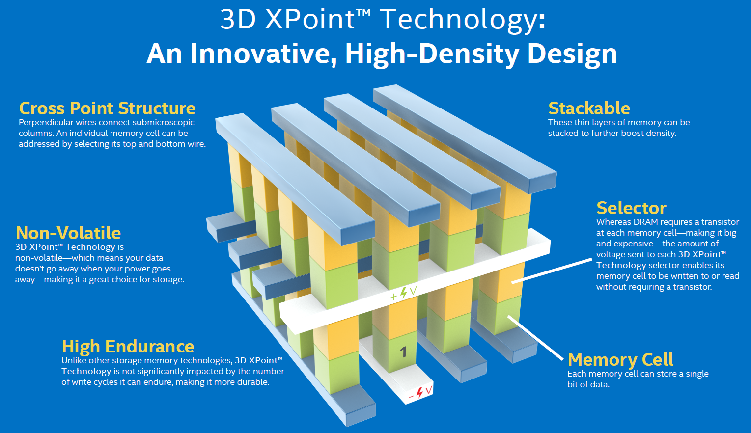
There are precious few details available as of yet on the architecture, but we do know that it consists of columns connected by a series of perpendicular wires in a cross point architecture. These columns contain a memory cell and a selector, but the real innovation is that unlike other technologies, which store data by trapping electrons in insulators (and other electron trapping techniques), 3D XPoint stores data by using the property change of the material itself. This bulk material property change utilizes the entire portion of the memory cell, which increases scalability and performance.
Get Tom's Hardware's best news and in-depth reviews, straight to your inbox.
The cross point layout, which connects each memory cell via bit and wordlines in a three dimensional checkerboard, is revolutionary. This allows each memory cell to be read/written individually. NAND has to erase large blocks of memory cells simultaneously. The cross point architecture allows for an exponential increase in performance, and Intel is currently building it on a 20nm process with a 128-Gbit density (or 128 billion memory cells per chip). 3D XPoint can be scaled at the node by shrinking lithography to sub-20nm, and also scaled in 3D by stacking layers higher. This will keep the cost of the memory low, though Intel and Micron did not provide specific price points. The companies did indicate that the price will fall between DRAM and NAND, which is an encouraging sign, because economics will dictate the success of this radical new technology.
Intel indicated the new memory would connect to the host system via the PCIe bus, which is yet another reason that Intel and Micron have been vocal proponents of NVMe. The NVMe protocol was designed from the ground up for non-volatile memory technologies, and not NAND in particular. Now it is apparent that Intel and Micron were laying the groundwork for something more as they developed the new protocol.
Speaking of economics, Intel and Micron are already producing the early generation of the new technology at the IMFT Lehi, Utah fab. However, they mentioned that both companies will also produce the memory separately, meaning they both have rights to the technology outside of the IMFT collaboration. This is an important nugget of information, because there is some speculation that the glory days of IMFT may be coming to an end in the next few years.
Both companies will produce end products with the technology, and they will not be licensing it to other companies. I doubt that Intel/Micron will sell the memory outside of their own finished products, but that is speculation. We do know that final products will be available in 2016, and neither company expects the new technology to affect their lucrative NAND business. The new technology will slot in between NAND and DRAM in use-cases, so it will not supplant either existing memory technology.
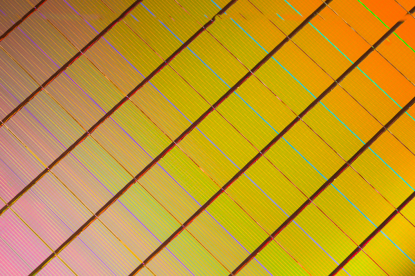
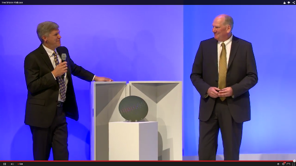
Intel's Robert Crooke, VP and GM NVM Solutions Group at Intel Corporation, and Mark Durcan, CEO of Micron, made the announcement together and took the chance to strike a pose with a 3D XPoint wafer. There has been rampant speculation as to which new technology would power the future for over 40 years. Pundits have projected that one of a whole host of technologies, including PCM, ReRAM, memristors, STT-RAM, among others, would emerge as the newest memory technology.
According to Intel and Micron, these questions have been answered, and 3D XPoint is the future. Frankly, this is a huge surprise, merely because 3D XPoint was completely wrapped in a cloak of secrecy until today. This is really a once-in-a-generation type of announcement, and the new capabilities will unlock the potential of future computing platforms, from mobile devices to the largest supercomputers. It will be interesting to see how other players, such as Flash Forward and Samsung, react to this development.
We hope to gain more information in the coming hours, so stay tuned for more analysis.
Paul Alcorn is a Contributing Editor for Tom's Hardware, covering Storage. Follow him on Twitter and Google+. Follow us @tomshardware, on Facebook and on Google+.
Edit: July 28th, 2015 4:40 PM --Corrected CEO name

Paul Alcorn is the Editor-in-Chief for Tom's Hardware US. He also writes news and reviews on CPUs, storage, and enterprise hardware.
-
sergeyn Hopefully when this thing is out Toms will not have problems with image resolution. I can't see anything of what's written on that slide.Reply -
derekullo This reminds me of RDRAM.Reply
"Both companies will produce end products with the technology, and they will not be licensing it to other companies."
Hopefully this won't be a repeat. -
jaber2 I never realized all this time memory was in 2D, this 3D is a game changer, some already claim they've already have been doing this, we might look at some patent claims before we see one in the market, also can't believe we've been on nand for the past 26+ yearsReply -
gangrel "The new technology will slot in between NAND and DRAM in use-cases, so it will not supplant either existing memory technology."Reply
Maybe for a few months. The FIRST thing I can see, given its properties, is allowing caching of HUGE amounts of data, for games, or for DB servers. How about "shut down but restart from here" PCs? How about re-imagining how an OS is deployed? Much of the OS is write occasional (updates), read many times.
-
Paul Alcorn I agree, this changes the whole paradigm, from Internet of Things to smart watches to laptops and phones all the way up to the datacenter. exciting times indeed!Reply -
gangrel Oh, gosh, yes. I forgot that point. The impact on small devices, be they tablets, phones, or watches, may be even more revolutionary.Reply
All of this presupposes that the price will be competitive, of course, but yield is a large factor here. If the stuff is hard to make at first, we can expect that will improve as the manufacturing process matures. And given the density, we're looking at potentially high yields with HIGH capacities. An interesting point is, SSDs at smaller capacities run a bit slower than the same drives at higher capacities...because the smaller drives use too few chips to use all the channels.
And IIRC, they were talking about doing this at about 20 nm. Imagine when (IF?) they can implement this at 10 nm, as that process gets finalized. -
salgado18 The two contradictions in the announcement:Reply
"and the new capabilities will unlock the potential of future computing platforms, from mobile devices to the largest supercomputers."
"Both companies will produce end products with the technology, and they will not be licensing it to other companies."
We can't really expect corporations to be nice people, after all they exist to make money, but still, true global progress will require more money, manpower, effort, and lots of wasted resources. -
Phillip ReplyHopefully when this thing is out Toms will not have problems with image resolution. I can't see anything of what's written on that slide.
Hit "Ctrl" and zoom in...oh wait...that makes it worse! :-)


