Chicago (IL) - With semiconductor structures getting smaller every two years, a switch to nanotechnology manufacturing is inevitable and a matter of time. Skyrocketing cost to build nano-fabs will have dramatic effects on the semiconductor industry and force chip companies to rethink their business model, suggests a new research report.
Most chip manufacturers are complaining already today about quickly raising cost to build new manufacturing plants for next-generations semiconductor products. Firms such as Intel spend between $2 and $4 billion for new locations. These investments do not only pave the way to new technologies, but also allows manufacturers to use new production processes and increase production efficiencies and ultimately improve profitability.
However, it is increasingly difficult for manufacturers to find the right compromise between investment and production efficiency. According to Lawrence Gasman, an analyst with market research firm NanoMarkets, the cost of a new fab could equal the cost of the GDP of small countries. This will get even worse with the introduction of fabs for new nanotechnology manufacturing processes and ultimately can disrupt current semiconductor business models. "There is no way that large semiconductor companies are going to escalate the current cost level with current manufacturing technologies," he said. According to Gasman, a fab could cost between $10 and $20 billion within a few years.
Moore's Law however is driving the industry to continue scaling processes of semiconductors and it is a matter of time when even more expensive nano-fabs will be needed. Gasman believes that the introduction of fabs that will use completely different manufacturing processes we know today will disrupt and separate the semiconductor industry. "The increasing cost of these plants could break the current semiconductor business model," Gasman said. "Chip manufacturers will have to look at their business and think about potential trade-offs." While larger firms such as Intel are likely to focus on more and more general purpose chips to boost production volume, smaller firms may be forced to specialize on smaller market segments or think about contracting manufacturers such as Taiwan Semiconductor: "We are certainly going to see a restructuring of the industry."
Gasman believes the semiconductor industry will have all tools in place for volume nanotechnology manufacturing by 2015, but it is unclear today which processes and materials may be the way to go. There are at least seven technology approaches today that aim to replace current CMOS processes, but each one appears to be facing major problems. For example, immersion lithography is not believed to be able to scale much beyond 32 nm, EUV lithography depends on currently unavailable 100w light sources, and nano-imprint lithography may only be suited for low volume production.
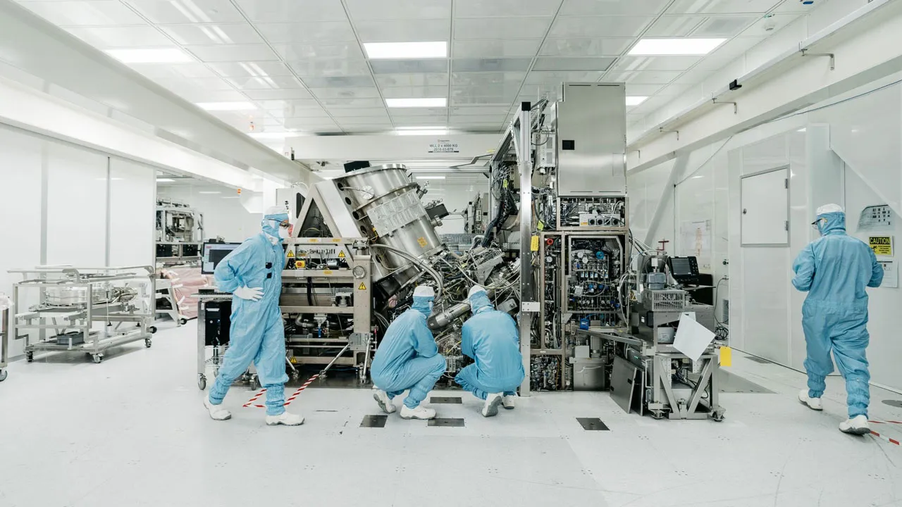
"While all the machinery for nano production is out there, none of these technologies is ready for volume production at this time," Gasman said. Current optical lithography is believed to be a viable option for semiconductor companies until 2013 and a production process of 22 nm or 16 nm, down from today's 90 nm processors. If Gasman is right, many semiconductor manufacturers will have to change their business models between then and now, simply for the reason to be able to stay in business.