Intel sees 65 nm transition on track, 450 mm wafers appear on horizon
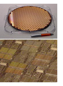
Hillsboro (OR) - Intel will send 65 nm chips into mass production by the end of this year and considers the technology as critical element for a lower power consumption of its future processors. The company also said it has taken initial steps in preparing a move from 300 to 450 mm wafers.
Intel remains confident that there will be no delays for the introduction of 65 nm chips with mass production scheduled to launch late this year and products to be available commercially early in 2006. According to Mark Bohr, senior fellow and director of process architecture and integration at Intel, the new development of the production process is on track with yield rates ahead of schedule, hinting to a smooth transition from 90 nm chips.
Compared to previous transitions, the move to 65 nm is less complex, at least as far as the introduction of new features is concerned. While the integration of copper in 130 nm chips and strained silicon in 90 nm products were considered to be disruptive compared to previous product generations, the new lineup includes just a second generation of strained silicon, according to Bohr. As previous production processes, the chips continue to be manufactured using 193 nm wavelength light, but Intel will implement a technique called Alternating Phase Shift Masks to be able to create 35 nm lines on wafers. Resulting gate lengths are 35 nm, accordingly.
While smaller structures typically increase leakage current, Bohr said that Intel was able to actually improve the relationship between transistor performance and leakage with 65 nm chips, if compared to the previous 90 nm generation. This allowed product designers either to scale performance of the processor faster or take advantage of an opportunity to decrease power consumption, he explained. A direct effect is likely to be seen in the mobile dual-core processor Yonah: According to Bohr, the scaling improvement "is a major contributor" that enables Intel to keep Yonah in the same power envelope as the currently shipping single-core Pentium M.
Bohr also said Intel was looking beyond the current chip production with 300 mm (12") wafer technology, which is still in its early stages. Mass production of chips on 300 mm silicon platters was launched in 2001 and currently accounts for about 20 percent of global chip output, according to figures released by Gartner. The research firm does not expect 300 mm wafers to become mainstream before 2009. Still, Intel is likely to introduce the next generation wafer shortly thereafter. According to Bohr, Intel is in early-stage talks to plan production on 450 mm wafers. A transition could be expected for the timeframe of 2011 / 2012 and beyond the production of 32 nm chips.
Changes of wafer sizes usually are closely tied to an improvement of the economical aspect of chip production. Material costs per wafer increase, but productivity typically grows. With the transition from 200 to 300 mm wafers back in 2001, Intel said production cost was reduced by about 30 percent and overall productivity climbed by a factor of four.
Get Tom's Hardware's best news and in-depth reviews, straight to your inbox.

Wolfgang Gruener is an experienced professional in digital strategy and content, specializing in web strategy, content architecture, user experience, and applying AI in content operations within the insurtech industry. His previous roles include Director, Digital Strategy and Content Experience at American Eagle, Managing Editor at TG Daily, and contributing to publications like Tom's Guide and Tom's Hardware.
