Lightmatter's Mars SoC Bends Light to Process Data
The era of laser-powered computing draws near
Slow transistors got you down? Just shoot lasers through silicon instead. That's the fundamental idea behind silicon photonics-based computing, and it appears to be coming closer to reality. Lightmatter takes that approach with its new Mars SoC that's designed specifically for AI inferencing workloads, but the tech could eventually bleed out to general-purpose chips. The company unveiled its working Mars test chip, which bends light generated from a laser to enable computation, at Hot Chips 2020. The chip touts some impressive specs.
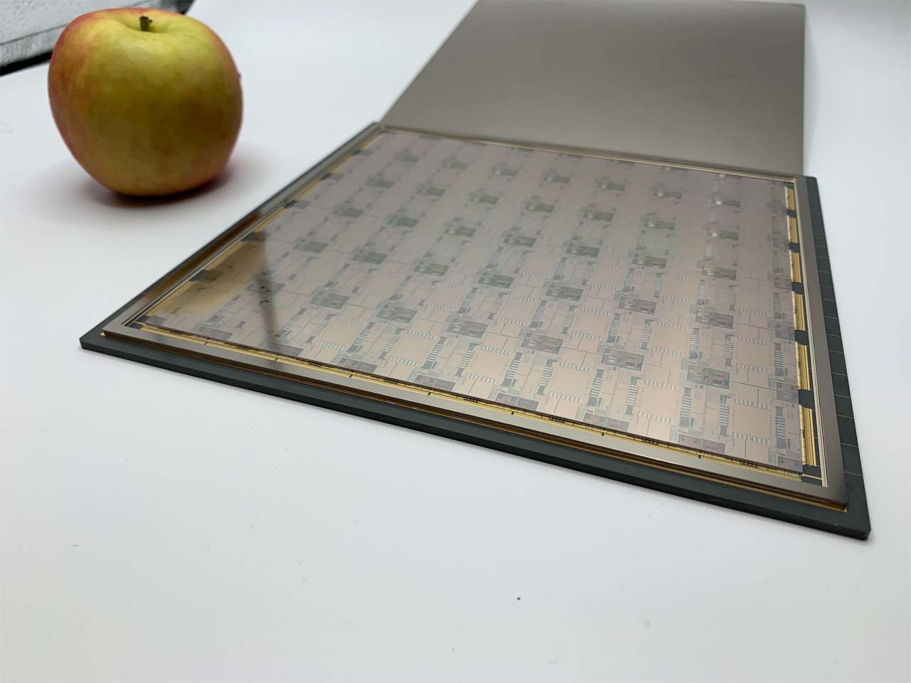
The new Mars SoC marks several fundamental steps forward that could bring optical computing closer to the mainstream, and the company even shared a picture of a large wafer-scale optical device (above) that could hold multiple SoCs (below).
Lightmatter claims the photonics core operates at the speed of light through an optical tensor core, boosting bandwidth by a factor of ten while reducing latency from the typical 100ns with electronics-based chips to a staggering 100 picoseconds (a 1000X improvement). The chip can be made with standard CMOS manufacturing processes, meaning it doesn't require exotic materials and can be made in existing fabs. Unlike quantum chips, it can run at standard temperatures, too.
Article continues below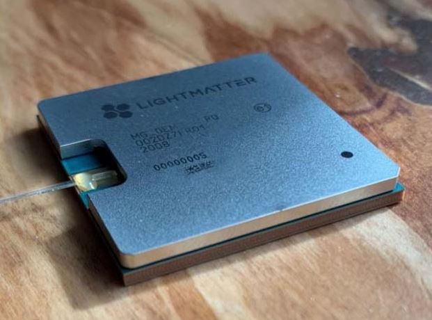
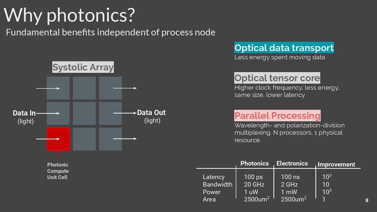
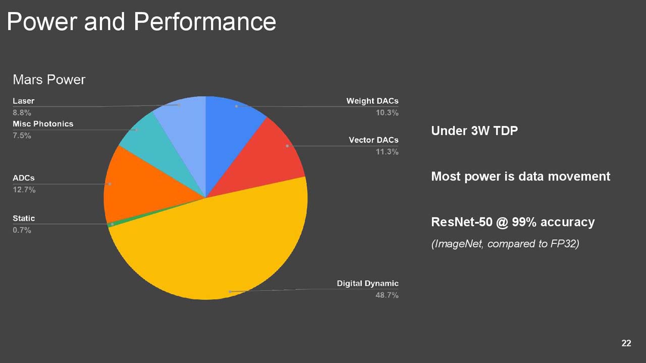
The core pulls only one microwatt of power, which is yet another 1000X improvement over the typical one milliwatt of power consumed by an electronics-based chip. The photonic module is part of a 3D-stacked device that includes a laser and a 14nm ASIC to handle digital work like I/O operations. The optical core itself uses almost zero power for computation, but zooming out to the SoC level, the entire device sucks a mere 3W under load. Lightmatter claims to have pulled off this feat within the same die area as a comparable transistor-powered chip – meaning it will be a similarly compact solution compared to a normal processor.
The Mars SoC sets the stage for radical advances in compute efficiency, but the company hasn't shared final performance data yet outside of saying the end product is three orders of magnitude faster than electronics-based devices. The finished SoC rides on a standard PCIe-attached test device for now. Still, the company teased a wafer-scale switched optical interconnect that could house multiple photonics units, and other elements like memory, connected via CoW (Chip-on-Wafer) 3D stacking. That means these chips are moving closer to actual use in the real world, and the company outlined a few future improvements that could lead to even more impressive performance in the future.
Lightmatter shared in-depth details of the design during its Hot Chips presentation, and we've down our best to boil it down to understandable terms below.
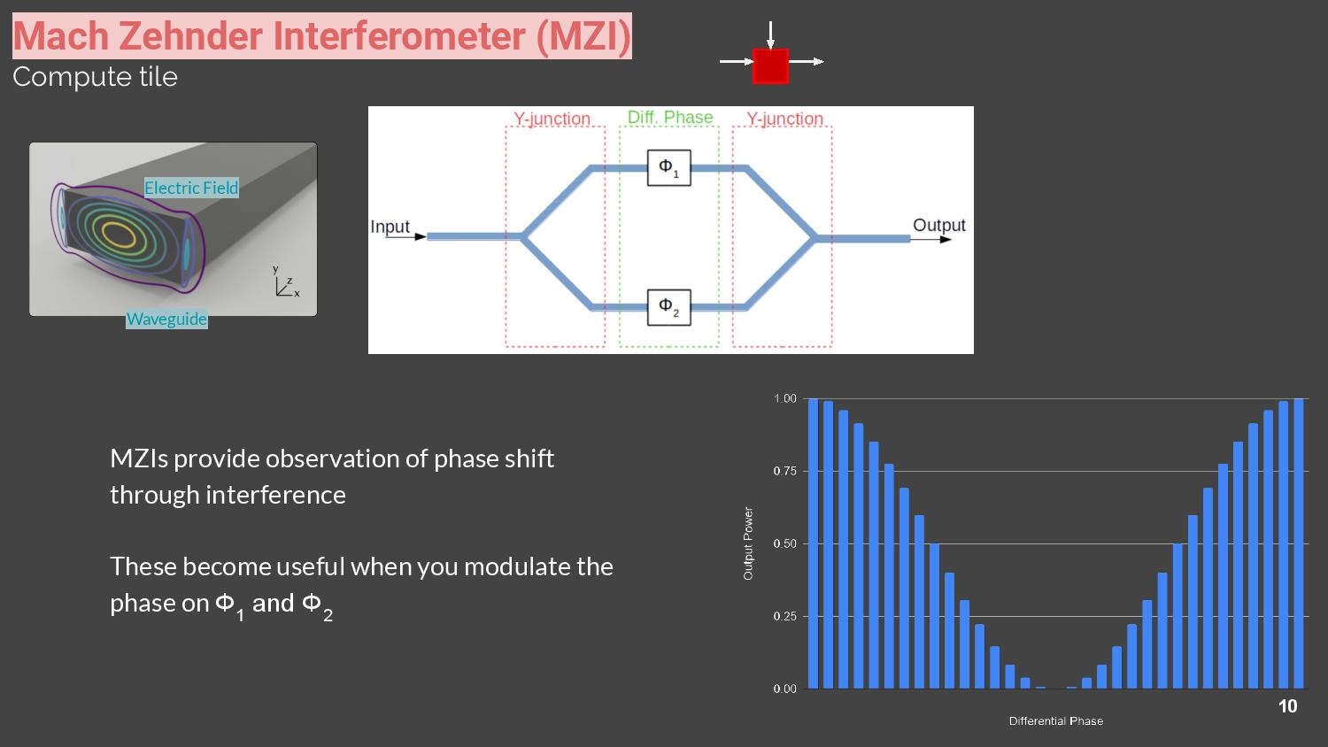
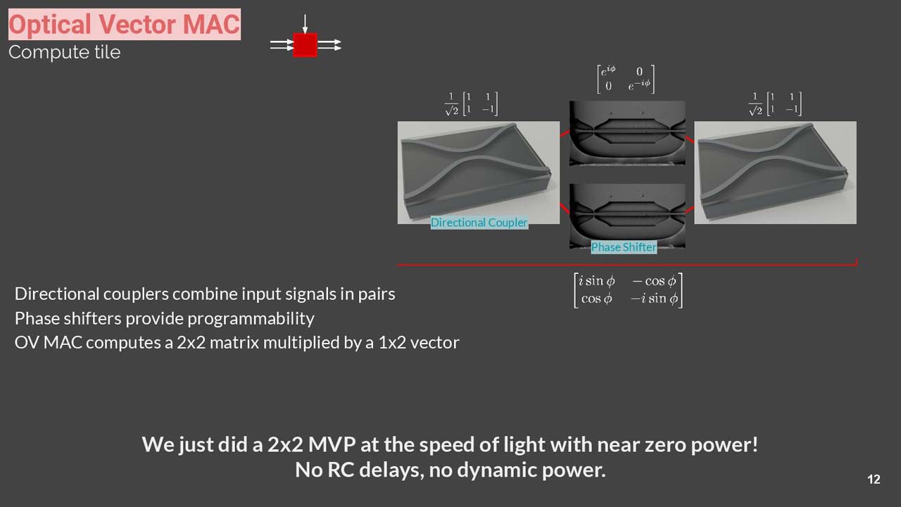
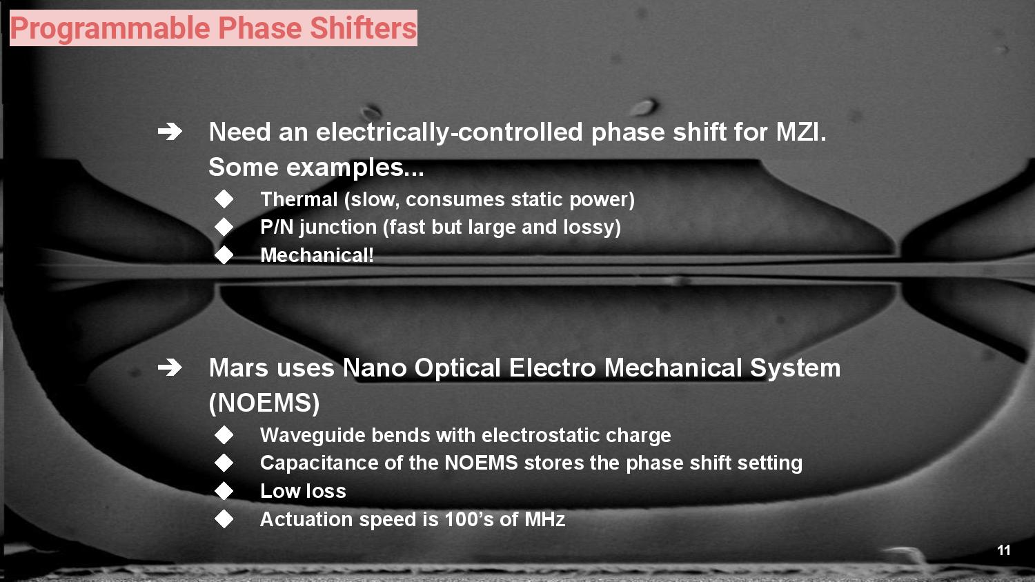
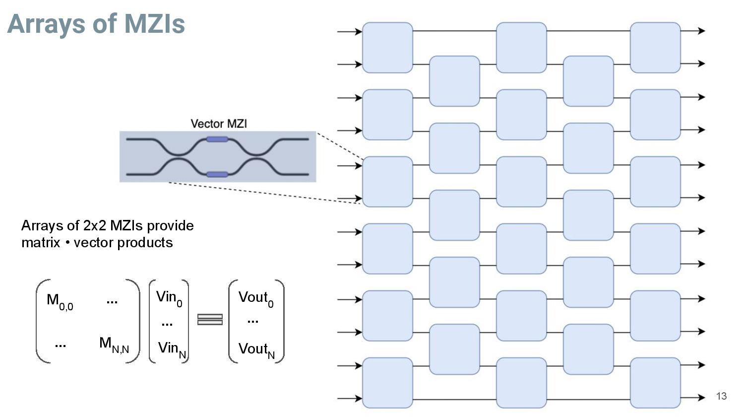
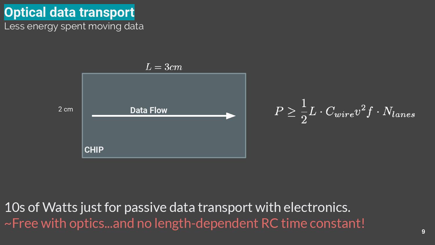
The rationale for switching to optical computing is pretty simple: The rate of frequency improvements from moving to smaller, denser process nodes has declined, so performance gains are becoming less pronounced with each new generation of chips. While we're approaching the fundamental limits of switching efficiency in transistors, photons don't have to play by the same rules. To reset the performance clock, Lightmatter created a multi-chip design that fuses the benefits of transistor density (it still uses an ASIC as part of the solution) with the speed and efficiency of optical computing.
Get Tom's Hardware's best news and in-depth reviews, straight to your inbox.
It all starts in the MZI (Mach Zehnder Interferometer, first image). A laser shoots a beam of photons into the device, which has a silicon waveguide that directs the light (yes, light can travel through silicon). The waveguide splits the stream into two beams, and the basic concept here is to create a different phase shift for each beam. This creates either a constructive or deconstructive interference when the two beams come back together at the end of the waveguide, which is then observed/measured as the output. Sounds simple enough, right?
The real innovation comes in creating the phase shifter. Lightmatter had a few options of how to do this, but found that simply bending the silicon waveguides, and thus the light traveling through them, creates a phase shift while still meeting the company's power and speed requirements. The company uses a nano-optical electro-mechanical system (NOEMS - yeah, that's a mouthful) to bend the waveguides in a pretty innovative way.
The waveguides are suspended in the air, and then a charge is applied to a group of surrounding capacitors, which causes the waveguides to bend. Lightmatter says this technique requires very little power ("nearly zero" - leakage is minimal), and the capacitors can operate at several hundred GHz.
With this basic building block in hand, the company creates more complex structures via directional couplers that combine input signals into pairs, with the end result being the ability to do matrix vector multiply functions.
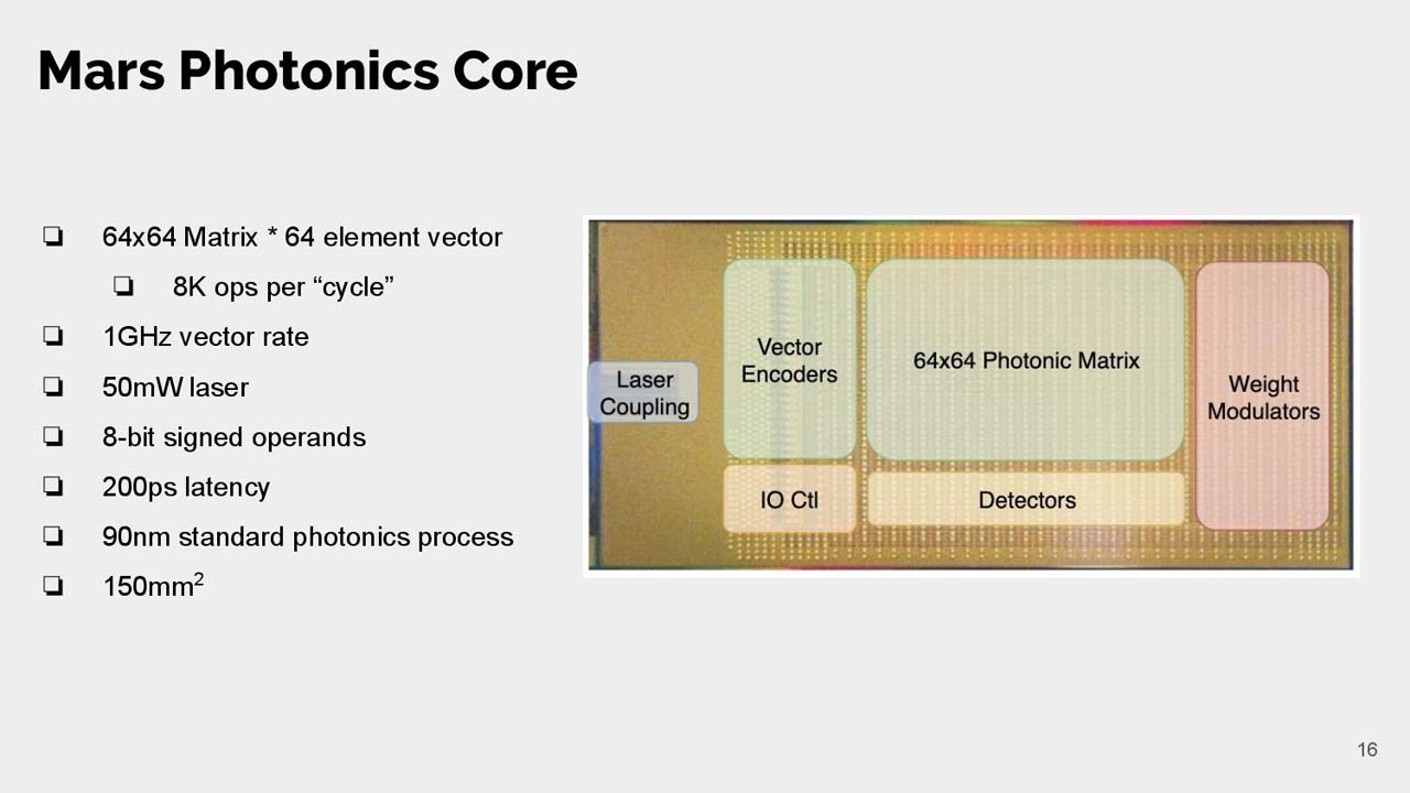
These structures are then combined into larger arrays (scales to 1000's) to create more computational power, and the latency of the data traveling through the arrays is, well, the speed of light. The end result is a 64X64 matrix * 64 element vector that can do a eight operations per (the equivalent of) a cycle. Lightmatter hasn't specified the overall clock speed, but says it is "GHz."
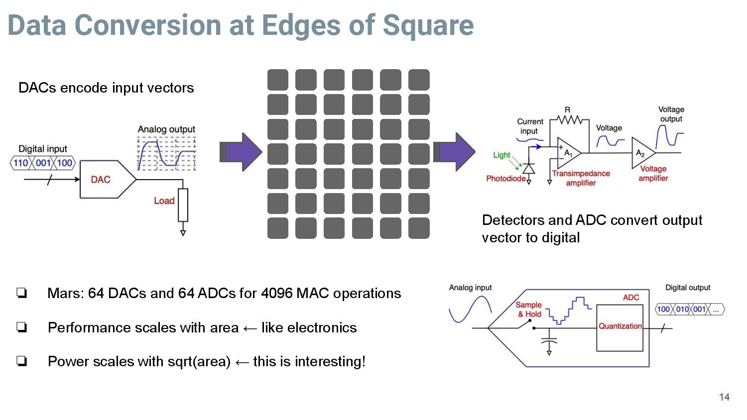
Bandwidth through the array weighs in at terahertz, so the other electronics in the device become the limiting factor. Data is fed into the device with a fairly standard technique of using voltage to manipulate the laser, and the light exiting the device is fed into a series of converters that bring it back into digital code. That's the obvious bottleneck, and conversion consumes most of the power for the end device.


The photonic devices' compute performance scales with area, just like in normal chips, so stacking up more arrays creates more performance. Latency also increases with more units, too, but Lightmatter claims it is still well under a nanosecond of latency for a 1000x1000 array of units, which is 3X lower than standard chips.
Power used inside the array is negligible, and while laser power is typically the largest contributor to power consumption in photonic chips, it only consumes a few milliwatts. Lightmatter says the only meaningful power consumption comes from converting the data to and from the optical signal, which happens on either side of the array.
In fact, adding more photonic compute units to the array increases efficiency - you get quadratic performance scaling compared to power consumption increases. In other words, adding a unit will give you four times more performance compared to the amount of additional power consumed. In contrast, performance and power scale linearly with standard transistor-based chips, so efficiency gains aren't as pronounced.
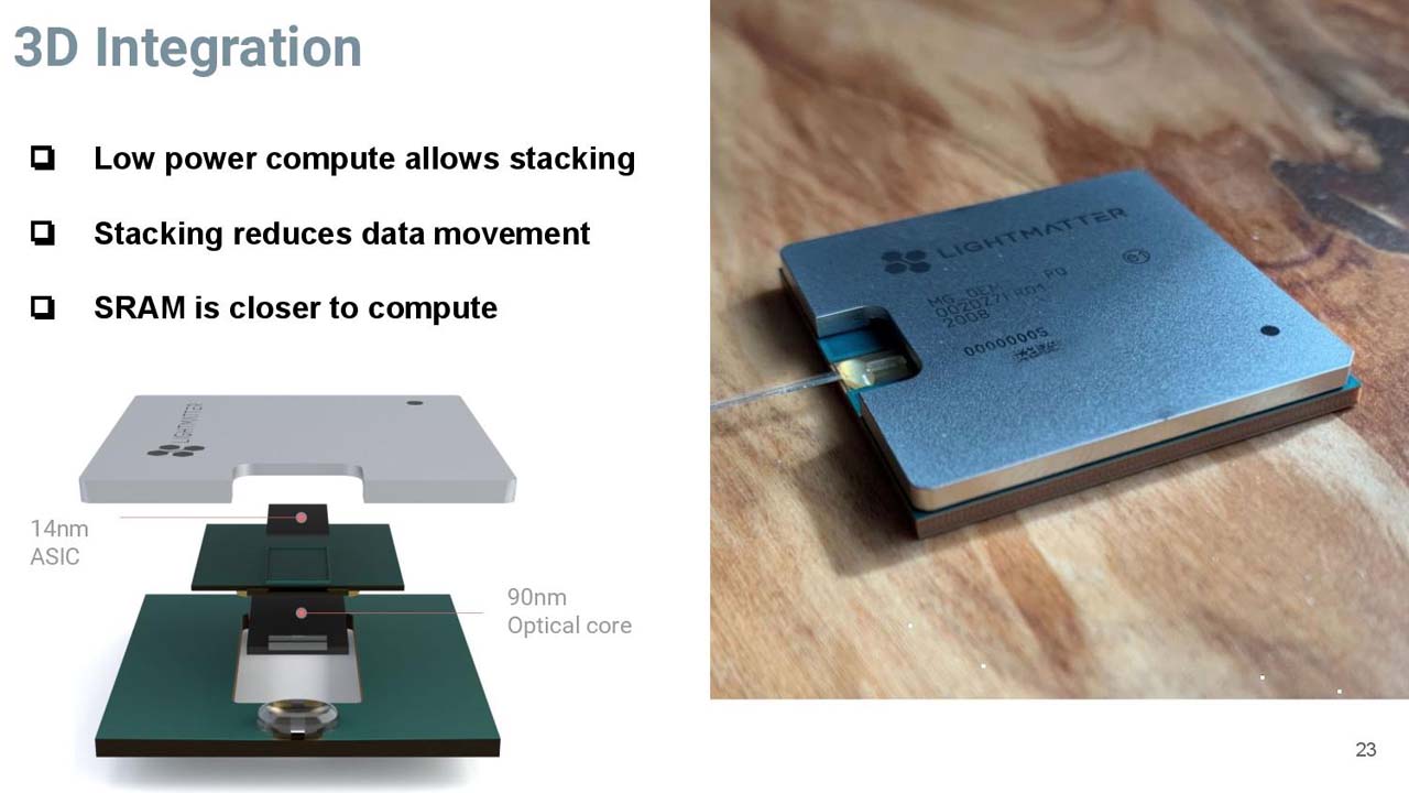
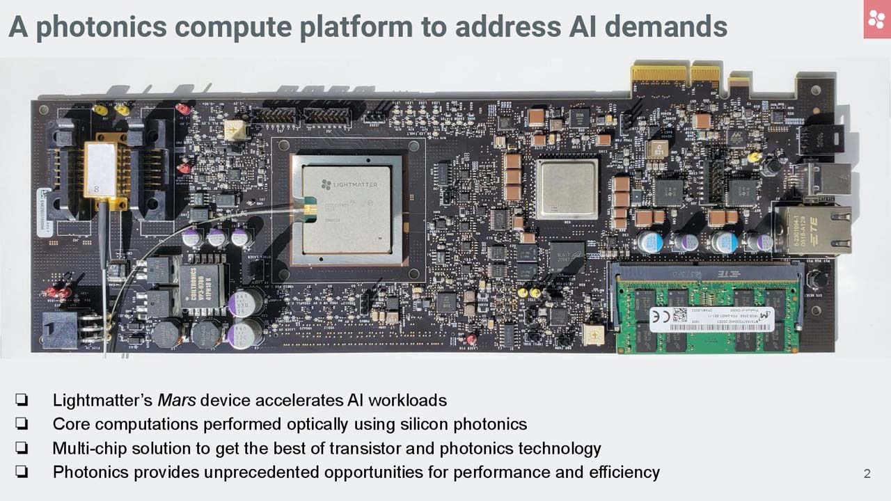

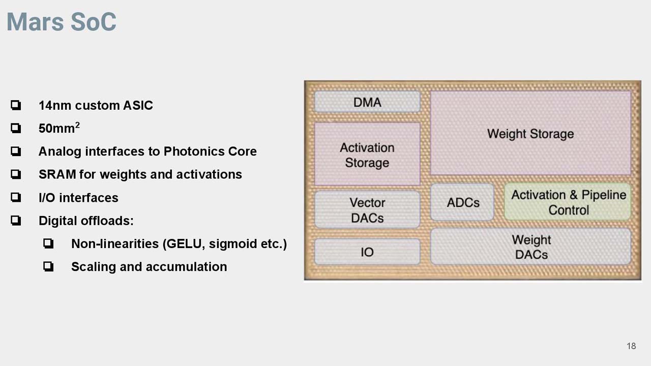
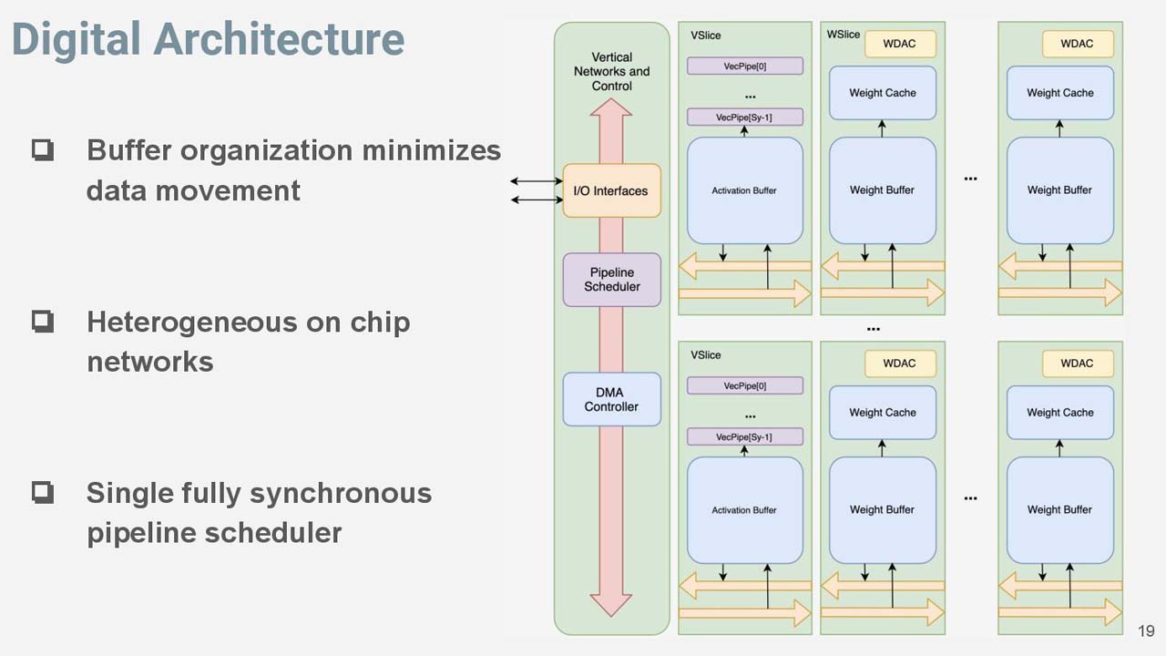
Lightmatter combines the 90mm2 photonic compute unit, which uses a standard GlobalFoundries 12nm photonic process, with a 50mW laser and a 14nm ASIC (50mm2, 30MB of SRAM) into a 3D-stacked multi-chip module. All connected by a low-power analog I/O interface that reduces data travel to 1mm.
The entire device measures 150mm2 and total latency measures under 200 picoseconds (that only includes analog and optical, not digital conversion). The ASIC handles some AI operations that the photonics core isn't well suited for, and also provides connections to external interfaces. The net effect is an SoC that has a 3W TDP, and it runs at standard data center operating temperatures.
For now, the test chip rides on a PCIe-connected device, but as shown at the top of the article, it will eventually ride along with many others on a massive wafer-scale dynamically switched optical interconnect. The photonics units will be mounted on the wafer using CoW (Chip-on-Wafer) 3D stacking. That will help address the power consumption concerns associated with data movement, which usually consumes more power than computation. Lightmatter claims that, using photonics, data transfers can be reduced from using tens of watts to single-digit microwatts.
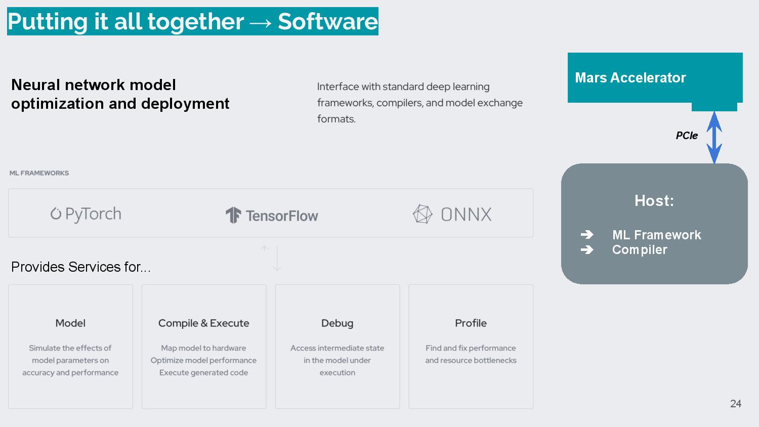
Lightmatter says the devices will interface with all standard deep learning frameworks, like TensorFlow, PyTorch, and ONNX, compilers, and model exchange formats.
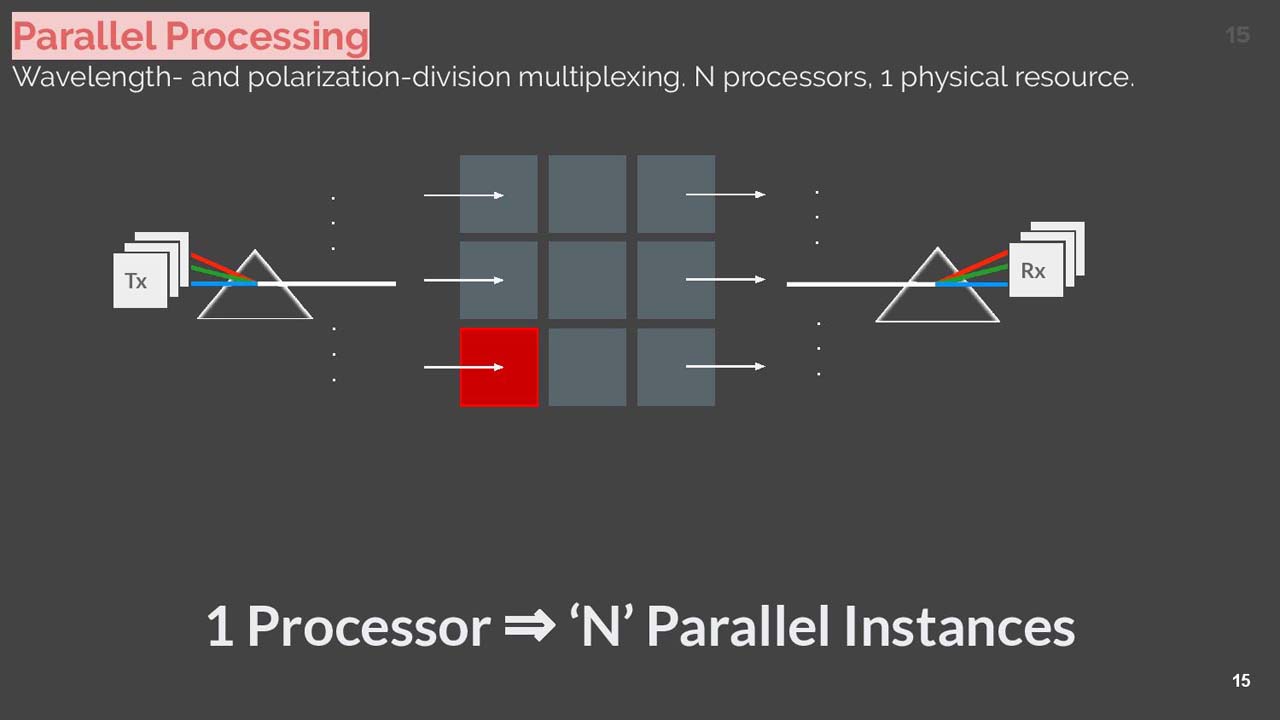
In the end, Lightmatter says the device is incredibly fast and power efficient, but there's room to grow, too. Even with today's fiber optic systems, different wavelengths and colors can allow encoding multiple streams of data into one stream, thus multiplying performance. Lightmatter says those same techniques could eventually be used in its photonics cores to multiply the performance of the device.
The dream of optical computing, at least in a cost-effective enough manner to see wide deployment, has long eluded the industry. Lightmatter's design uses standard CMOS manufacturing techniques, so it could conceivably be etched out on standard wafers. If the product makes it out of the lab, naturally, we'd expect the leading devices to be quite expensive, but those could be offset with power savings in both computation and data movement.
The company hasn't shared hard performance data yet, instead saying the solution is three orders of magnitude faster than electronics-based solutions, or final clock rates, but says it plans to share more information as it works its product closer to market. Lightmatter says that production units arrive in the fall of 2021.

Paul Alcorn is the Editor-in-Chief for Tom's Hardware US. He also writes news and reviews on CPUs, storage, and enterprise hardware.
-
Endymio While "computing at the speed of light" has a jazzy ring to it, the fact is that electrical impulses move at roughly the same speed as light anyway. The purported advantages of this chip appear to come mostly from the fact that, computationally, this seems to be essentially an analog tensor core, rather than digital. Nice, if you're building an AI cluster ... but I don't see this replacing a general-purpose CPU any time soon.Reply -
everettfsargent "In fact, adding more photonic compute units to the array increases efficiency - you get quadratic performance scaling compared to power consumption increases. In other words, adding a unit will give you four times more performance compared to the amount of additional power consumed. "Reply
... should be ...
"In other words, adding a unit will give you THREE times MORE performance compared to the amount of ADDITIONAL power consumed. "
!00% is already baked into 1X and 400% is baked into 2X (quadratic), therefore reword that sentence because 400% - 100% = 300% MORE performance compared to the amount of ADDITIONAL power consumed, 2X -1X =1X.
You all can't even do 2-bit calculations correctly!
Oh and I can't wait for my 16-bit tensor overlords sometime after 2100 CE. Unicorn hardware. -
Endymio Reply
Actually, it's correct if the word "more" was simply meant to be "the". As in "four times THE performance".everettfsargent said:... should be ...
"In other words, adding a unit will give you THREE times MORE performance -
everettfsargent ReplyEndymio said:Actually, it's correct if the word "more" was simply meant to be "the". As in "four times THE performance".
Still doesn't work!
"4X THE performance compared to the amount of ADDITIONAL power consumed, 2X -1X =1X. "
Double the power quadruple the performance, now that makes perfect sense. -
recycledelectrons ReplyEndymio said:the fact is that electrical impulses move at roughly the same speed as light anyway.
I disagree.
Real electrical wires are not ideal conductors or even ideal resistors. They also have some capacitance. That makes the circuit an RC circuit, also called a RC delay circuit. It takes time to charge the capacitor. -
OpticsinComputing The numbers presented were worse than what can be achieved with conventional digital electronics at equivalent bit depth.Reply -
Chung Leong ReplyEndymio said:Nice, if you're building an AI cluster ... but I don't see this replacing a general-purpose CPU any time soon.
I imagine the tech can be used to massively boost ray-tracing performance. -
Endymio Reply
And? You don't think this photonic chip is an ideal vacuum either, do you? Assuming its effective IOR is similar to a fiberoptic thread, then signals and both it and an electrical wire are going to move at approximately the same speed: 0.6-0.7c.recycledelectrons said:I disagree. Real electrical wires are not ideal conductors or even ideal resistors. -
margrave Reply
If "roughly" means around 60%, then sure. Electrical signals generally move around 60%-ish of light speed. But people here have been picky about 4x more vs. 3x more. So i'll be picky by saying 60% is not "roughly the same as".Endymio said:While "computing at the speed of light" has a jazzy ring to it, the fact is that electrical impulses move at roughly the same speed as light anyway. The purported advantages of this chip appear to come mostly from the fact that, computationally, this seems to be essentially an analog tensor core, rather than digital. Nice, if you're building an AI cluster ... but I don't see this replacing a general-purpose CPU any time soon. -
grimfox I wonder if there is a security benefit given the "alien" nature of the light processor. Could you use something like this to create a sort of firewall between a secure storage (say for biometric data) and the host system?Reply
I also see some benefits in networking. Imagine having your long haul fiber drop directly into a processor and then get distributed to sub fiber networks without having to convert down to electrical signals and back up to light again at each node. Could shave a few MS of latency off your transcontinental or transoceanic transmissions.
Similarly, would it be more immune to radiation? Space probes with GHz processors or satellites that could survive in close orbit around Jupiter and Saturn for long periods.
Seems like there could be some potential there. Hopefully they can keep developing the tech and unlock some of it.