Self-Assembling Chips Could Push Production Limits
Researchers have found a way to enable the creation of circuitry with self-assembling rectangles.
Get Tom's Hardware's best news and in-depth reviews, straight to your inbox.
You are now subscribed
Your newsletter sign-up was successful
If the technology finds its way into commercial production, devices such as memory or processors could be produced faster and scaled down to smaller structures. The approach could also lead to storage products such as hard drives with greater capacities.
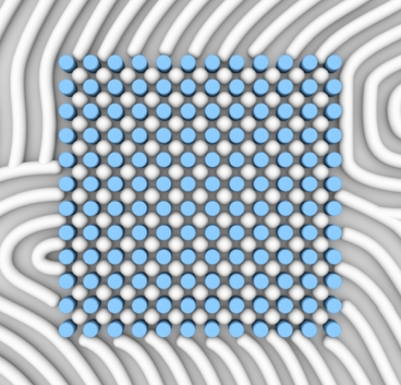
The method, developed at MIT by visiting doctoral student Amir Tavakkoli of the National University of Singapore, as well as two graduate students and under the leadership of three professors, the team was able to force self-assembling polymers not to create hexagonal shapes, but squares in the form of an array of tiny posts on the surface that guides the patterning of the self-assembling polymer molecules. The researchers found that they could use the same approach to build a variety of shapes of the material itself, including cylinders, spheres, ellipsoids and double cylinders.
Karl Berggren, co-author of a published paper and associate professor of electrical engineering at MIT, said that the team was able to achieve those shapes since “the template, which is coated so as to repel one of the polymer components, causes a lot of local strain on the pattern. The polymer then twists and turns to try to avoid this strain, and in so doing rearranges on the surface. So we can defeat the polymer’s natural inclinations, and make it create much more interesting patterns.”
Article continues belowBesides a possible time-to-market advantage the self-assembling method could have over electron-beam lithography (due to the fact that multiple shapes and patterns can be created simultaneously), the researchers said that their technology could also deliver finer chip structures with twice the feature density. It is a seen as a possible solution to integrate much more circuitry on any given space of a microchip. However, the self-assembling method is not limited to semiconductors. Magnetic media could also benefit from a much more granular pattern.
Contact Us for News Tips, Corrections and Feedback
Get Tom's Hardware's best news and in-depth reviews, straight to your inbox.

Douglas Perry was a freelance writer for Tom's Hardware covering semiconductors, storage technology, quantum computing, and processor power delivery. He has authored several books and is currently an editor for The Oregonian/OregonLive.
-
Onus Now all we need to do is engineer a bacterium to poop out this stuff. Hmmm, didn't Michael Crichton already describe something like this?Reply -
Albyint First we have self repairing nano circuitry demoed last year, then those little atom bots that continually add to themselves to make themselves more efficient, now we have self building computer chips. This does mean our cyber overlords are nearing completion!Reply
All hail the Oligarchy of Steel! >_> -
f-14 tick tock and moore's law.Reply
god forbid that this process gets patented and stolen by apple, samsung, blah blah blah kevin parrish and douglas perry will have a collective apoplexy with their communist/borg approach to technology.
had to tweak their noses, they do deserve it. -
supall Moore's law continues...!Reply
I'm starting to think MIT is controlled by some sort of complex AI that is steering the course to robot domination with all of their inventions. -
A Bad Day jtt283Now all we need to do is engineer a bacterium to poop out this stuff. Hmmm, didn't Michael Crichton already describe something like this?Reply
Last year or so, a group of researchers got some algae specie similar to Coccolithophore to build a microchip die into their shells. Once the algae dies off, you harvest the shells.
I wonder if calcium compounds are going to affect the transistors though. -
deksman MaxTeslaSkynet Skynet SkynetWe are all going to die.Reply
What the frack is with people making these idiotic claims that computers are going to take over and kill us?
Oh right... its a byproduct of BAD hollywood movies that deal in fantasy and not science.
For the love of man people, show some capacity for critical thinking and stop projecting movies into reality.
-
deksman supallMoore's law continues...!I'm starting to think MIT is controlled by some sort of complex AI that is steering the course to robot domination with all of their inventions.Reply
Lol...
Moore's law is nothing more than a business model that caters to capitalism and profits... apart from that, it has NOTHING to do with our technical capability or efficiency because we already had the ability to produce much more powerful, faster, fully upgradeable, extremely efficient computers since (at least) 1997.
I'm amazed at how people have the capacity to think that what we see in the market today (planned obsolescence) is the 'best' what we can do (far from it).
