TSMC Arizona allegedly now producing AMD's Ryzen 9000 and Apple's S9 processors: Report
Fab 21 Phase 1A is ramping up production.

Get Tom's Hardware's best news and in-depth reviews, straight to your inbox.
You are now subscribed
Your newsletter sign-up was successful
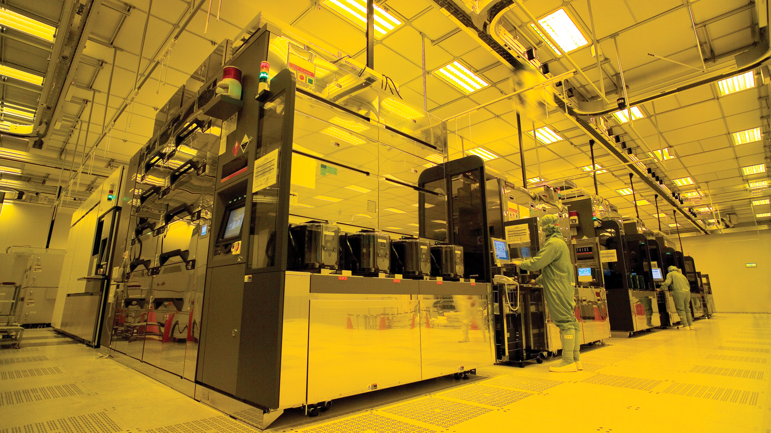
TSMC's Fab 21 in Arizona is gradually ramping up production, and recently it began to manufacture some of AMD's Ryzen 9000-series processors for client PCs as well as some ingredients of Apple's S9 system-in-package (SiP) for smart watches, reports Tim Culpan, a well-connected journalist, citing his own sources.
If the information is accurate, then TSMC's Fab 21 in the U.S. is now producing at least three chips: Apple's A16 Bionic system-on-chip for iPhone 15 and iPhone 15 Plus smartphones, at least one IC in the Apple S9 SiP for smart watches (we presume this is the actual application processor with two 64-bit cores and a quad-core neural engine), and one of AMD's Ryzen 9000-series CPU. All of the said processors are made using TSMC's 4nm-class N4 and N4P technologies.
Tim Culpan reports that TSMC makes "Grand Rapids" CPU for AMD and this is certainly not a codename that we have heard of before. It is entirely possible that AMD uses a previously unknown silicon — perhaps featuring specific capabilities and aimed at select applications — to test TSMC's Fab 21 in Arizona. However, it makes more sense to test a new fab with a familiar silicon. Moreover, considering that Culpan sources are from Taiwan and a lot of communications happen verbally, it is possible that some of the sources made a slip of the tongue and called Granite Ridge as Grand Rapids. Granite Ridge is of course a familiar silicon for AMD.
TSMC's Fab 21 phase 1 is projected to officially start operations in the first half of 2025 and Culpan reports that by now all the tools in the Phase 1A have been installed and are being used to make chips. At this point, production capacity of the facility is 10,000 wafer starts per month. However, Phase 1B is 'facing tooling bottlenecks,' according to Culpan. This does not necessarily mean delays as some tools may be installed earlier and the others later. However, this clearly affects capacity as Phase 1B reportedly has a capacity of 14,000 WSPM.
As it turns out, Fab 21 is still understaffed, according to Culpan. This week, TSMC internally invited Taiwan staff to apply for a few hundred roles in Arizona, including fab operations and equipment installation, Culpan reports citing his sources. While the company aims to prioritize local hiring, this move reflects the challenges of staffing the new facility. Despite local hires now outnumbering foreign (Taiwanese) staff in Arizona, pulling hundreds from headquarters highlights the ongoing difficulties.
Get Tom's Hardware's best news and in-depth reviews, straight to your inbox.

Anton Shilov is a contributing writer at Tom’s Hardware. Over the past couple of decades, he has covered everything from CPUs and GPUs to supercomputers and from modern process technologies and latest fab tools to high-tech industry trends.
-
bit_user This is one reason I think AMD might've opted to use N4 for Zen 5 CCDs and maybe even RDNA4 GPUs. I wouldn't go so far as to presume it's why Nvidia stuck with an N4 node for Blackwell, but maybe.Reply -
Jimbojan Isn't Intel doing 3nm? Thus, Intel's product is far more power efficient; going into 18A, no one can compete, not even ARM's product, like Apple'sReply -
TCA_ChinChin Reply
Does this have anything to do with evading tariffs? Or just companies investing in a node that has lots of (domestic and otherwise) availability?bit_user said:This is one reason I think AMD might've opted to use N4 for Zen 5 CCDs and maybe even RDNA4 GPUs. I wouldn't go so far as to presume it's why Nvidia stuck with an N4 node for Blackwell, but maybe. -
Elusive Ruse Reply
“Evading” has a negative connotation, implies they are trying to hide the origin of the product’s manufacturing location. The word you are looking for is “avoiding”.TCA_ChinChin said:Does this have anything to do with evading tariffs? Or just companies investing in a node that has lots of (domestic and otherwise) availability? -
spongiemaster Reply
Nvidia did it to save money. Same reason they are rumored to be looking at Samsung for their next architecture.bit_user said:This is one reason I think AMD might've opted to use N4 for Zen 5 CCDs and maybe even RDNA4 GPUs. I wouldn't go so far as to presume it's why Nvidia stuck with an N4 node for Blackwell, but maybe.
https://semiwiki.com/forum/index.php?threads/is-tsmc%E2%80%99s-2nm-chip-out-of-the-running-two-key-reasons-why-nvidia-and-qualcomm-join-hands-with-samsung-are-exposed.21794/ -
bit_user Reply
Intel is believed to be using N3B, which is a first-gen 3nm TSMC node. The efficiency data between Intel's Lunar Lake & Arrow Lake vs. others is out there, if you look for it.Jimbojan said:Isn't Intel doing 3nm? Thus, Intel's product is far more power efficient;
That's going to be Panther Lake, initially. We shall see how it compares.Jimbojan said:going into 18A, no one can compete, -
bit_user Reply
I hope Taiwan isn't going to get hit with tariffs, but we'll see. I think the main benefit is securing availability, in the event that Taiwan goes offline.TCA_ChinChin said:Does this have anything to do with evading tariffs?
Based on what's been reported about TSMC charging more for wafers from their AZ plant, I think they'd still be more expensive, even if the N4 wafers from Taiwan got a 10% markup added to them.