Tachyum's ‘Industry’s First Universal Processor’ Gets $25 Million in Funding
Silicon start-up Tachyum has completed a Series-A funding round that has given it a $25 million war chest. The company unveiled its Prodigy Universal Processor family last year at Hot Chips and plans to tape out the chip this year with a launch in the second half of 2020. It claims the chips outperform CPUs, GPUs, and TPUs, all while still being programmable like a CPU and consuming 10x less power.
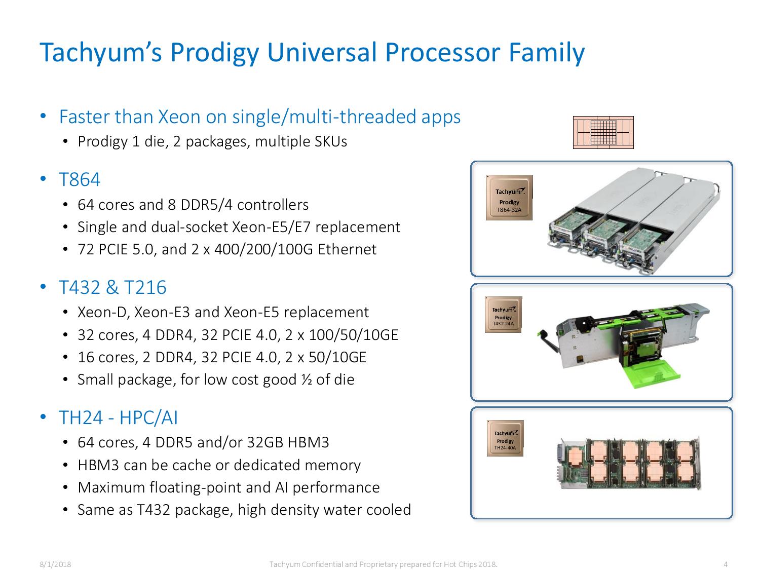
Tachyum makes impressive claims for its Prodigy line-up that it claims are faster than Xeon and smaller than ARM chips. It claims higher IPC than the Skylake architecture (which is found in all of Intel’s Core chips since late 2015), and in a much smaller chip, too. Built on TSMC’s high-performance 7nm process, like AMD’s Zen 2 family, the 64-core die measures just 290mm2. For comparison, AMD’s Rome has eight 8-core chiplets of 74mm2 for 592mm2, and also a large accompanying I/O die, totaling over 1000mm2 of silicon real estate for the 64-core product.
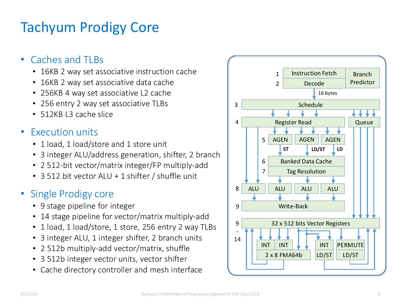
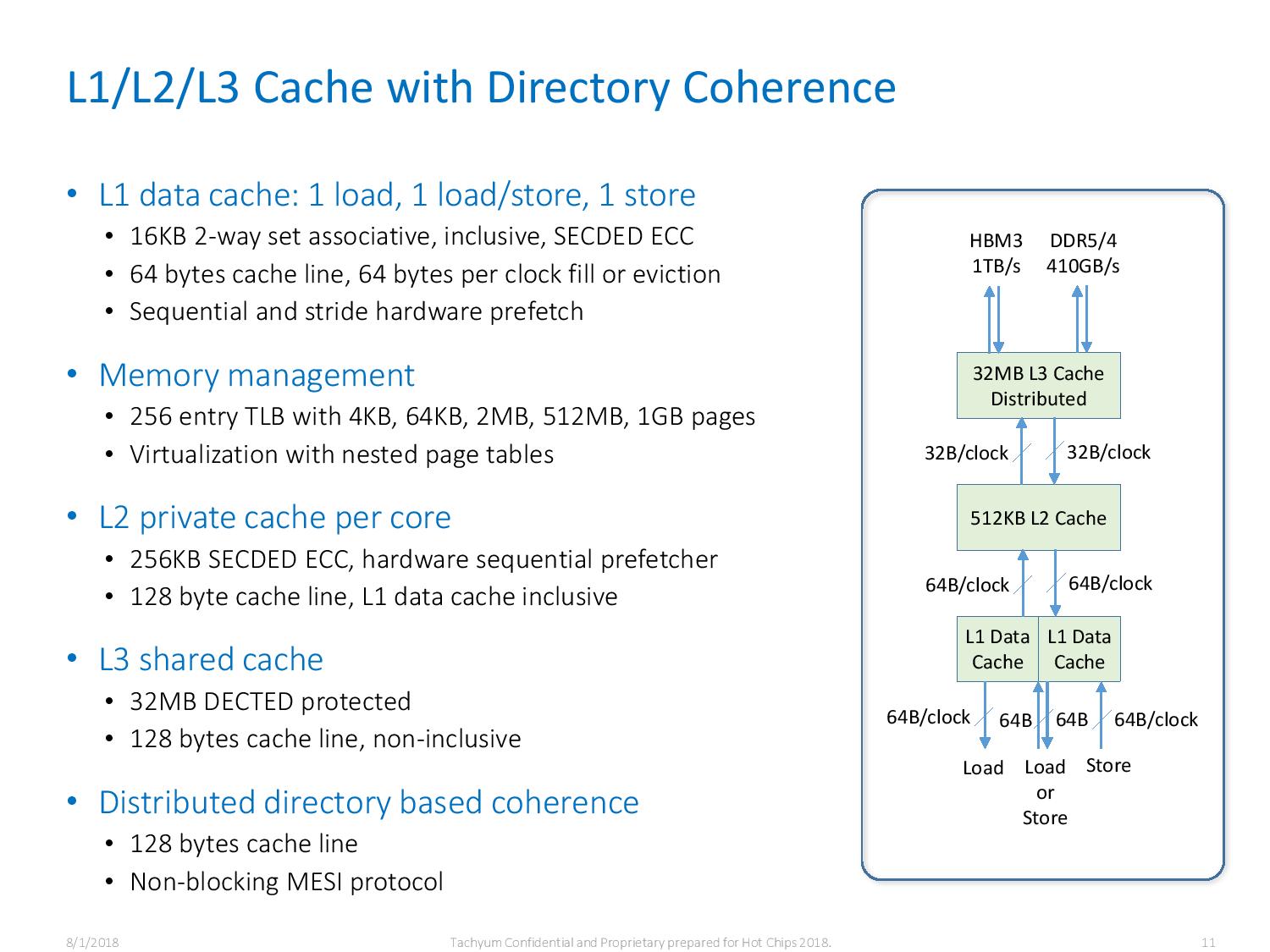
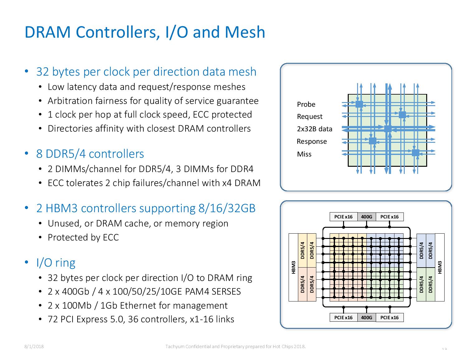
Furthermore, the chip has 8-channel DDR5 support and 72 PCIe 5.0 lanes, it supports 2x 400G Ethernet and HBM3 is optional. The chip is a bit lacking on the cache front, though, with just 32MB of fully coherent L2/L3 cache, but that is understandable given its small die size. That shouldn’t take away from its performance: despite packing 64 cores, they should run at an impressive 4GHz frequency, even during HPC and AI workloads, with just 180W of power consumption. Like Skylake-SP and Cascade Lake-SP, Prodigy has two 512-bit vector (floating-point) units per core, twice the width of Zen 2.

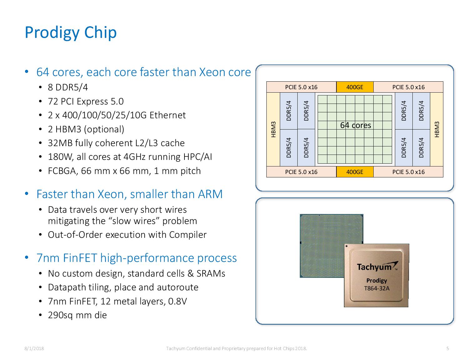
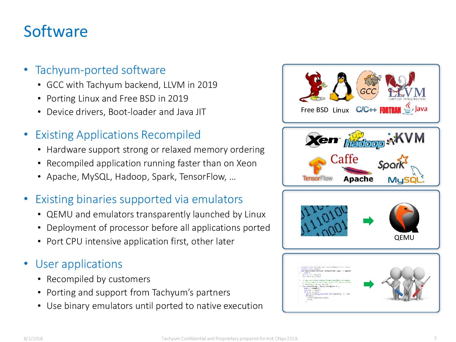
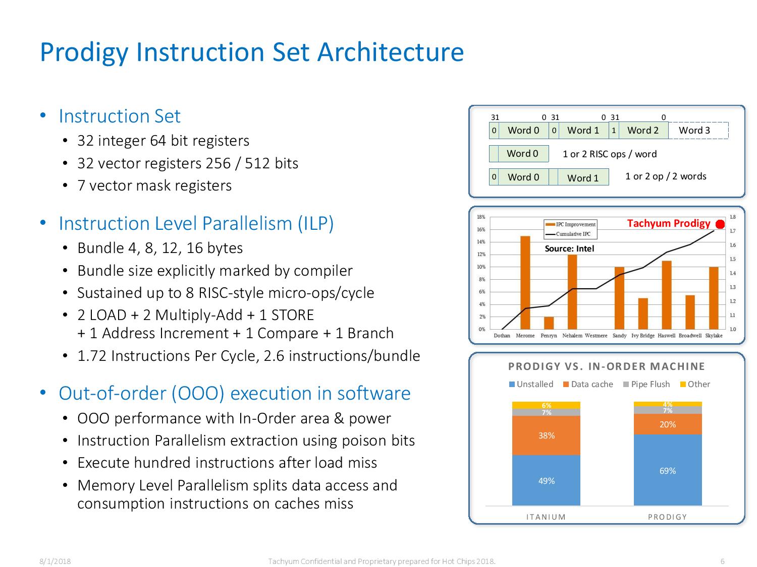
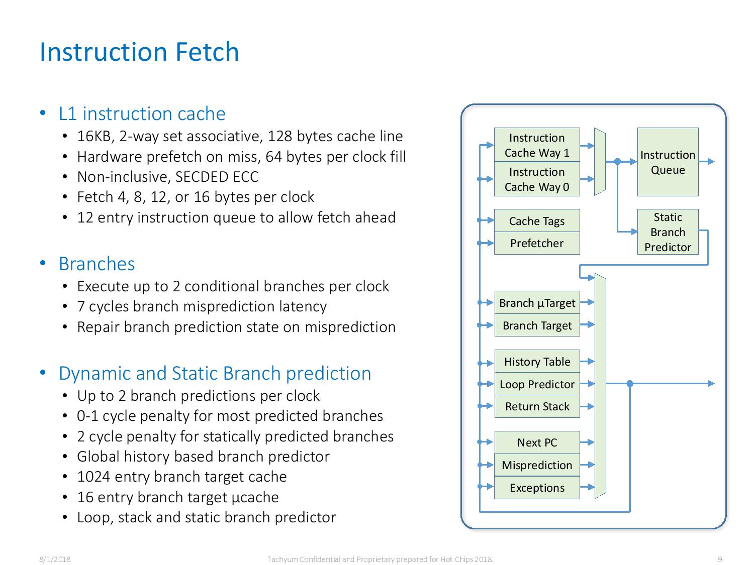

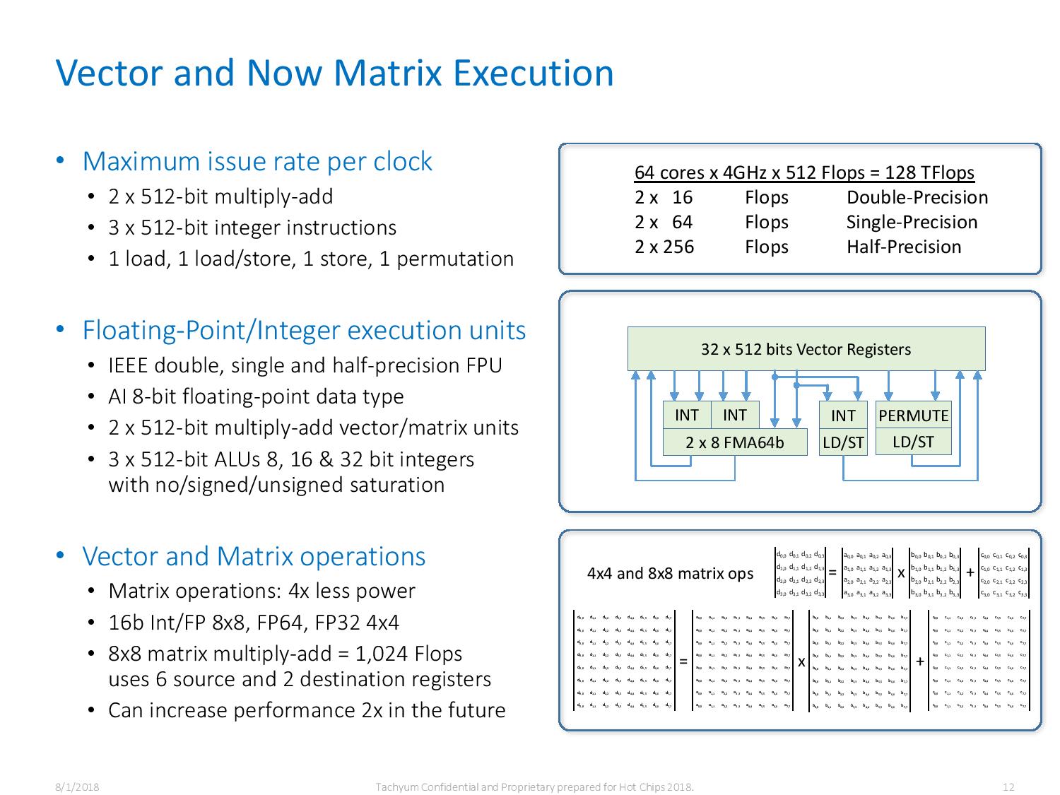

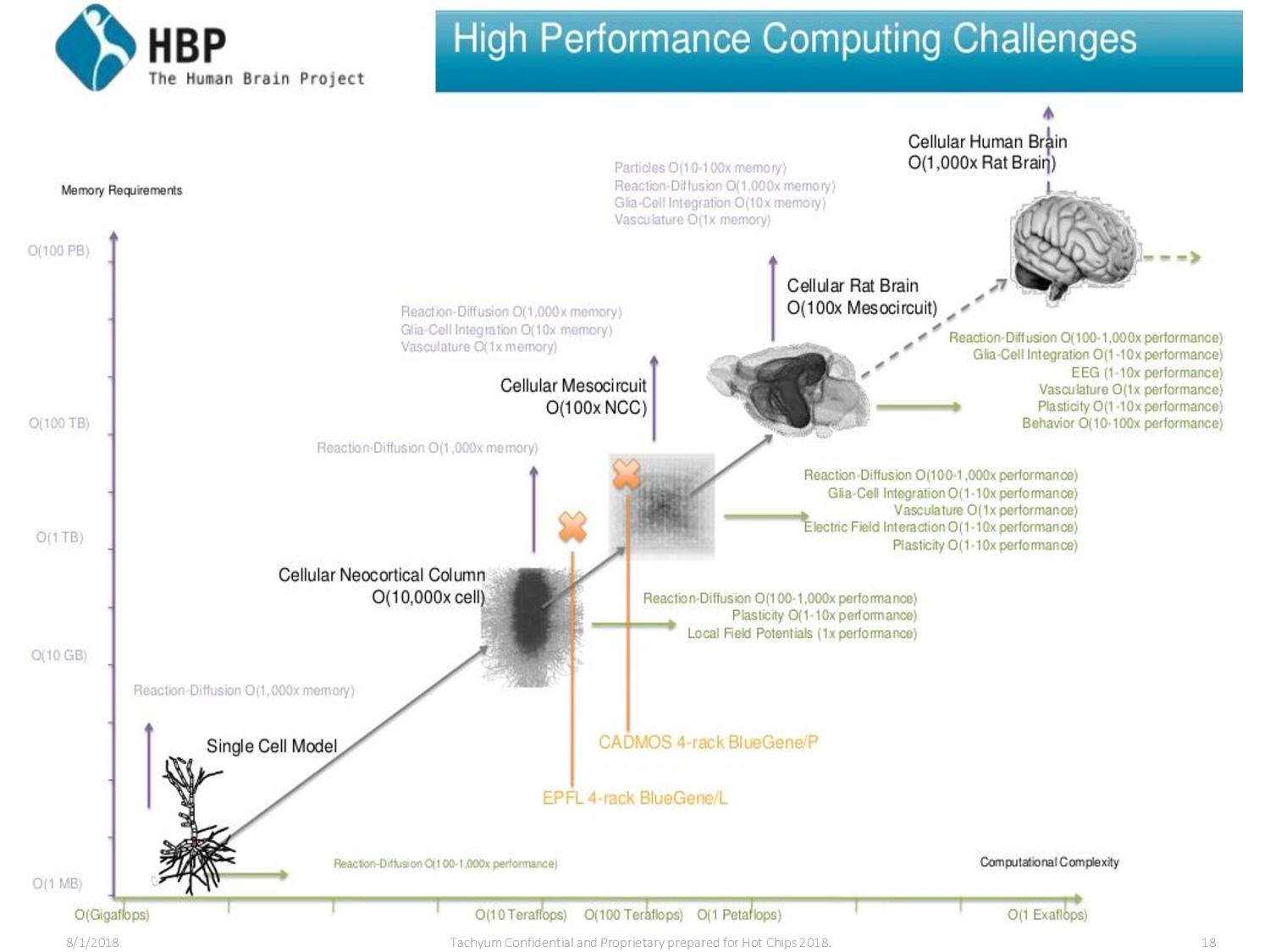
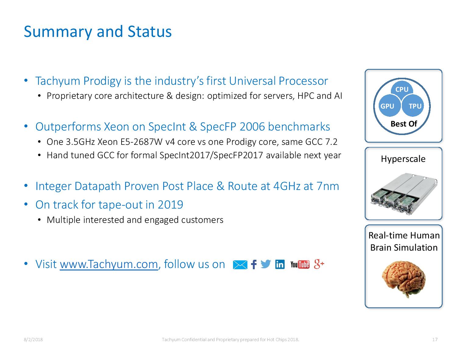


To the initiated, these would seem like unbelievable claims. Tachyum gives a few more details of how it has managed to do this, though. It says data travels over very short wires, mitigating the “slow wires problem.” Its main feature, however, looks to be its out-of-order execution (one of the primary design elements of state-of-the-art CPU architectures) in software, done by the compiler in advance instead of at run-time. This makes the core small. This, we note, is a euphemism for a Very Long Instruction Word (VLIW) instruction set architecture, like Intel’s Itanium. We also note that Itanium has never reached much success, to use a euphemism too. In any case, existing applications will have to be recompiled.
All in all, Tachyum claims it has developed a ‘universal processor’ in a time when it is fashionable to accelerate everything with heterogeneous chips or chiplets. It purports it has 10x lower power and server footprint, and 3x lower cost. Tachyum expects to bring its chip to market in the second half of 2020. It has also talked about the possibility of building an exascale system in 2020 with 250,000 of its Prodigy chips.
Get Tom's Hardware's best news and in-depth reviews, straight to your inbox.
-
Giroro "It claims the chips outperform "Reply
They claim the chips WILL outperform. Future tense. They barely got funding, so they haven't actually designed or built anything yet, so anything they claim right now are just a wishlist of hypothetical design goals.
At this point, they can basically say whatever they want. -
TJ Hooker Reply
Apparently Tachyum has been around since 2016, I would assume they have a foundation of design work in place. It's not like they only sprung into existence and started working on this after the series A funding round completed. Which makes sense, because otherwise there's no way they'd be taping out this year and coming to market next year.Giroro said:"It claims the chips outperform "
They claim the chips WILL outperform. Future tense. They barely got funding, so they haven't actually designed or built anything yet, so anything they claim right now are just a wishlist of hypothetical design goals.
At this point, they can basically say whatever they want.
Not to say I'm not highly skeptical of their claims though. -
southernshark Well we've never seen crazy claims made by a startup before, so it must be the real deal.Reply -
bit_user IMO, $25 M is a pretty small series-A funding round, for a chip startup.Reply
The chip is a bit lacking on the cache front, though, with just 32MB of fully coherent L2/L3 cache, but that is understandable given its small die size. That shouldn’t take away from its performance
Um, what? Performance across a sufficiently broad range of benchmarks is certainly affected by cache size!
Based on the slides, this seems like a VLIW with branch prediction. In just about every other respect, it looks a heck of a lot like Xeon Phi (KNL). That apparently didn't do too hot, as it's now a goner.
While I agree that we need to move beyond x86, which has gotten too cluttered with legacy instructions and relies too much on energy-intensive hardware-assist to run at high speeds, I'm not sure this one is going to come out on top. I think they'll get a few design wins in EU-based supercomputers, but I'm skeptical that the big cloud players are really going to take any big risks with such a small upstart, and I'm not sure their architecture includes enough of the potential efficiency wins.
Also, the clock speed is definitely too high to beat Nvidia's tensor cores and purpose-built AI chips. You get better energy efficiency at lower clocks, which allows GPUs to run much larger dies, in a roughly similar power envelope. With the net effect being better efficiency and far higher throughput.
History is littered with the bones of promising, next-gen HPC/hyperscale CPUs that have gotten much further than these guys. Some of the more recent casualties include SiCortex and Tilera.
https://en.wikipedia.org/wiki/SiCortexhttps://en.wikipedia.org/wiki/Tilera -
bit_user Reply
In supercomputing, there seems to be quite a lot of custom-loop water cooling and fully-immersive solutions.Jeppe Geer said:180W on a 290mm² die is going to call for some interesting cooling solutions.
Anyway, Vega 20 (from Radeon VII and the Instinct MI60) is ~300 W in 331 mm^2. So, they can probably use conventional forced air cooling with a vapor-chamber-based heatsink, like high-end GPUs have adopted. -
steelfox This guys remember me TRANSMETA ,I bet if they have luck they will sell the developed ips to AMD and Intel for some million dollars .Reply
