Repairing an Acer E5-521 Laptop: A Case Study
Synchronous Rectification Buck Regulator 101 (And A Cure)
Very few devices in modern PCs are powered directly from 12V or whatever the main power distribution rail voltage might be. Instead, point-of-load switching regulators are in charge of creating voltages where they are needed, the majority of which being of the “buck” (voltage reduction) variety, as all digital circuitry in contemporary systems operate on 2.5V or less.
To figure out what a 0.02Ω short to ground means, a brief overview of how buck regulators work and how they may fail seems in order. Multi-phase regulators work the same way; they simply split current between multiple pairs and inductors to reduce losses, facilitate cooling, and increase the effective switching frequency to simplify filtering.
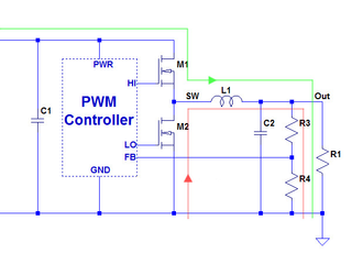
A buck regulator’s fundamental operating principle is simple: a top switch (M1) turns on to allow energy to flow from the source to the load (R1) following the green path when the output voltage is below the intended value. An inductor (L1) stores the energy associated with the voltage difference between the input and output in the form of a magnetic field, and the output capacitor (C2) further helps smooth out the voltage output. Once the target voltage is reached, M1 turns off and M2 turns on to provide a path along the red line for the inductor’s current to flow through so it can dump the surplus energy it stored into the load. This “free-wheeling” device is necessary as current through inductors does not want to change quickly (think of it like inertia for moving objects) and will generate whatever voltage is necessary to maintain a path until its energy is depleted, which is why you often get angry sparks when you hot-unplug heavily inductive loads from their power source. If you are wondering what C1’s role is, it represents the local supply bypass capacitors necessary to mitigate effects from wiring inductance and resistance, a simple but still vital task for stable and reliable operation. In simpler terms, the inductor averages the current while the capacitor averages the voltage with the top switch’s duty cycle setting the output voltage.
With ideal components, constant input voltage and constant output load, the steady-state output voltage would be given by VOut = VIn × TOn / T. In practice, though, many different types of losses (wiring and component electrical resistance, skin effect, on-resistance, switching transients, cross-conduction, etc.) significantly reduce that result. Most loads aren’t constant, either. Therefore, a regulator circuit with feedback is required to compensate for all of those factors.


What does that translate to in terms of circuit waveforms? The first simulation is a near-ideal synchronous rectification buck converter (take my schematic above and replace the FETs with a pulse generator, a necessary simplification as running simulations using FETs introduces some unnecessary distractions) operating at 500 kHz from a 12V supply and 10% duty cycle to feed 1.2V into a 0.1Ω load via a 10µH inductor and 22µF output capacitor. You can see inductor current (yellow trace) rise quickly when the switching node goes high and fall much more slowly as the inductor’s stored energy gets transferred to the load. To me, the most interesting part of these waveforms is the output filter capacitor’s ripple current: little more than 200mA peak to peak and 65mARMS on the capacitor under a 12A load. How is that interesting? The “common wisdom” says that heavy power supply load puts more strain on capacitors. In reality, under heavy loads where buck regulators are deep into “continuous mode” operation, inductors provide practically all load current while the capacitors are mainly there to absorb transients and noise. In my second simulation, I eliminated the capacitor altogether and only got 30mVPP of ripples, good enough for most digital loads were it not for transients.
What Can Possibly Go Wrong?
With basic operation out of the way, let’s talk about potential failure modes. In a synchronous buck converter, there are five groups of components to worry about: the input filter capacitors, the output filter capacitors, the inductor, the switches, and the pulse-width modulation regulator. How do these typically fail and what are their effect on regulator operation?
Capacitors
Capacitors have three common failure modes:
Stay On the Cutting Edge: Get the Tom's Hardware Newsletter
Join the experts who read Tom's Hardware for the inside track on enthusiast PC tech news — and have for over 25 years. We'll send breaking news and in-depth reviews of CPUs, GPUs, AI, maker hardware and more straight to your inbox.
- Electrolytic capacitors most often fail open-circuit, which is typically caused by either mechanical strain breaking a lead or the lead’s connection to the aluminum foil within, or loss of electrolyte in the form of pressure relief vents breaking open as is the case for the capacitors shown here, withering their effective capacitance to nothingness over time. When electrolytic capacitors fail, bulk decoupling is greatly reduced, increasing ripple voltage, noise, and crippling transient response. This is by far the most common failure in personal computer power supplies, monitors, and TVs. In most cases that I have seen, readily observable symptoms begin with occasional random shutdowns and progress from there until the device won’t turn on.
- Multi-layer chip capacitors (MLCC) are comprised of dozens or even hundreds of thin metal sheets separated by equally thin ceramic plates and typically fail shorted either due to defects or breaks in the separator plates, or contaminants getting past the end-cap seals causing corrosion across plates. Both failures can originate from manufacturing defects, moisture ingress during storage, thermal shock during board reflow, wave soldering damaging the plates or seals, and rough handling. Post-manufacturing, liquid damage is what causes the most issues with MLCCs as electrolysis corrosion eats away at the end caps and eventually breaks the seals, hence the importance of removing all power from wet electronics before that has a chance to happen. The heavily corroded or even missing end caps are a giveaway for MLCCs that suffered liquid damage while those that failed from manufacturing defect or mechanical damage may not show any obvious visual cues. Can you guess what happened to the MLCC shown here?
- Tantalum capacitors are notorious for spontaneously combusting or exploding to protest against abuse. They have fallen out of favor in consumer electronics with the advent of ultra-low impedance aluminum capacitors and affordable high-capacity MLCCs.
Inductors
Manufacturing defects notwithstanding, adequately sized inductors should never fail under normal circuit operation. Even so, they still have two typical failure modes:
- Blown open due to an over-current or weakness in their wiring, in which case you simply get no output as the path from input to output no longer exists. From what I have heard, many MacBook models are notorious for blowing up their inductors faster than they can blow the fuses meant to protect them.
- Internal short-circuit between turns of their winding due to defects in the wire’s enamel coating, mechanical damage, mechanical wear, or overheat burn-off. When turns short to each other, the inductor becomes a transformer with a shunted winding, drastically lowering its effective value due to the combination of reduced effective number of turns (inductance is proportional to N2) and the shorted secondary’s reflected low resistance appearing in parallel with the primary. If you lose 10% of an inductor to an internal short-circuit, you lose as much as 19% of the nominal inductance on the “primary” with a shunt winding possessing potentially as little as 10% of the resistance. If the original inductor was 10µH with 10mΩ of resistance, the primary will now be 8.1µH with 9mΩ of resistance, while the secondary will be a 1mΩ shunt. The formula to transpose loads from secondary to primary for an otherwise ideal transformer is ZP = ZS(NP/NS)2, which translates into an 81mΩ resistor appearing in parallel with the primary, dramatically increasing its losses. Efficiency goes down the drain as you are effectively dealing with a switching linear regulator at this point, ripples get much worse, and the load may get destroyed. Of course, a real-world accidental or wear-induced short is unlikely to be down into the milli-ohm range, which makes this example more of an absolute worst-case scenario. In my simulation here, the average voltage is still around 1.15V, but the inductor’s internal short has effectively turned it into a resistor, eliminating most of its ability to regulate current and allowing the output to peak at 3V. With this hypothetical inductor now dissipating 158W to deliver 15W, it is only a matter of seconds before it either desolders itself from the board or turns into a magic smoke signal generator until it blows open.
Before anyone points it out, I did omit the primary’s resistance in my overlaid schematic to save space.
MOSFETs
Semiconductors in general have only one failure mode: when they fail due to an over-current or over-voltage condition, the semiconductor’s hot spots melt, fusing internal layers together into a short-circuit. When semiconductors “blow open”, it mainly happens after an internal short pulled enough current to burn the bond wires between the leads and the die or, in some cases, the package leads themselves acting as fuses. If you have seen bright green flashes coming from a power supply, those would be from copper plasma arcs of such a catastrophic failure, typically on the primary side which has more stored energy available to vaporize components along with the necessary voltage and current to sustain arcs until a fuse blows or a breaker trips. As I previously mentioned, two switches are involved in a synchronous rectification buck regulator, so let’s have a look at what their failure means for their loads.
- The top switch is the gatekeeper between the source and the load. If it fails open, the input to output path is broken and no power can get to the load. If it fails shorted, as it usually does before going open from blowing its bond wires or leads, the output ends up connected directly to the input minus the inductor’s and FET’s resistance. This is one of those cases where you are very likely end up with a blown-open inductor and dead loads unless there is some other sufficiently fast over-current protection device upstream from M1 to cut power off.
- The low-side “free-wheeling” switch (M2 in previous schematics) is responsible for keeping the inductor’s current flowing to the load during the top switch’s off-time. When it fails shorted, you get little to no output as the switching node tied to ground and may blow the top side switch or fuse. In the more exciting case where it somehow blows open, the inductor will bring the switching node’s voltage down to whatever voltage is necessary to keep current flowing until it is done dumping its energy. In the case of a FET top switch, the inductor drags the M1’s source voltage below the gate (control) voltage and M1 is forced into its linear (partially on) region, dissipating the energy stored in the inductor. In my simulation here, M1 turns on and builds up current as usual when the switching node goes high but when it attempts to turn off, the inductor drags the switching node (M1’s source) to -5V resulting in a 5V effective gate-source voltage forcing M1 to conduct enough to let the inductor’s 12A continue to flow through with that extra 5V of drain-source voltage on top of the source’s 12V. If you attempted to drive the gate to -10V to prevent this from happening, the inductor would simply drag M1’s source to -15V in this instance. With most of the inductor’s energy getting dumped into M1, the duty cycle had to increase from 10% to 36.5% to maintain the same 1.2V/12A (14.4W) output, at which point M1 is dissipating 130W. From here, it would be a matter of seconds before M1 fails from extreme overheating with a high probability of taking out the load in the process.
PWM Controller
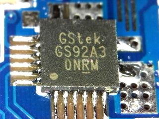
Switching voltage regulators come in all shapes and sizes with various degrees of integration, ranging from single-phase controllers requiring external components to drive external switching elements found in older power supplies to highly integrated multi-phase, multi-rail regulators integrating all switches and only requiring external filter components (ubiquitous in modern mobile devices). As with all other semiconductors, PWM controllers hardly ever fail on their own when operated within their rated limits and when they do fail for whatever reason, they favor shorting some number of things together leading to countless possible failure scenarios. Here, we’ll have a quick look at the most common ones.
- All integrated circuits need power and ground with whole metal layers within the chip dedicated to this purpose in more complex designs, which puts power and ground within microns of just about any fault within the die. If anything goes wrong and causes a dielectric breakdown or hot spot meltdown, the highest probability outcome is a short across the regulator’s power input and ground until the short blows clear or power cuts off from somewhere further upstream. In the case of the regulator shown here, bond wires acted as fuses and burnt a hole through the package.
- The next most common failure is one of the outputs getting stuck, be it due to the output drivers having failed shorted to either power or ground, or some other upstream failure within the chip causing it to stop switching. Driver outputs may also go floating or weak, which would leave the FETs partially on. Whatever the case may be, a stuck or weak driver output would quickly lead to FET failure unless the failure happened to be the high-side driver being stuck off, in which case there is no power to make anything else fail.
- Although not technically a PWM failure, excess ripple and noise on the controller’s power supply can cause the integrated circuit to misbehave from noise pickup or repeatedly re-entering under-voltage lock-out. If you have had a computer or other device randomly refuse to turn on or randomly shutting down, this may be what you are dealing with. One typical example of this failure pattern is my Antec SL300 PSU Repair where dead capacitors on the 5VSB output and the auxiliary rail powering the main controller prevented it from reliably turning on.
There are several other sources of PWM controller issues and the bulk of them involve external components like the timing capacitor, where a failed cap may either shut down the controller or cause it to operate at frequencies beyond the circuit design’s capabilities. A capacitor failing shorted in the voltage feedback circuit could cause the regulator to crank output voltage far out of specifications or mess up phase margins, which would in turn cause the output to have trouble settling after transients. A bad boost capacitor in designs using a high-side N-channel driver would prevent the controller from properly turning the high-side switch on and overheat it to destruction. This is by no means an exhaustive list. Basically, every component is sort-of-critical in its own way and given enough time, everything that can possibly go wrong eventually will.
Hunting For A Short
When you take a few minutes to think about every little thing that could possibly go wrong in a typical switching converter and consider the fact that a modern PC easily contains dozens of them, it puts into perspective how incredibly reliable each individual component involved in power regulation and distribution needs to be. In the specific case at hand, we are interested in the scenarios leading to a dead short across the system supply rail.
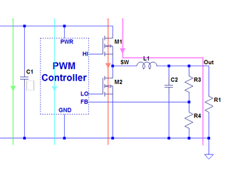
Since the resistance between the system power rail and ground is lowest in the immediate vicinity of the core voltage switching regulator, there must be something wrong in that neighborhood, and there are only four possible paths this short-circuit can take:
- Through C1, along the green arrow
- Through the PWM controller, following the cyan arrow
- Through M1 and M2 both shorted, following the red arrow
- Through M1 and the load both shorted, following the pink arrow
With the fault resistance being in the order of 20mΩ, we’re looking for the most direct and "hardest" path between supply and ground. While shorted semiconductors may be able to produce low resistances, the relatively low power nature of the PWM controller and its driver output only needing to deal with very short current pulses is unlikely to have heavy enough bond wires to short all the way down to 20mΩ. Power semiconductors like the FETs are better candidates for this. But achieving such low failure resistance would require a substantial drain-to-source weld in both devices, which is also unlikely. What are we left with? A failed load and high-side switch combination wouldn’t get to 20mΩ either as this scenario includes the inductor’s wiring resistance and a longer overall path. I did measure resistance from the inductor to both system rail and ground, both were over 700Ω, so definitely no short either way there. That leaves the local bypass capacitors on the input side as the prime suspects.
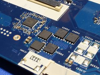
Can you spot the problem in this picture? I missed it the first few times I looked. It's the clearest image I have from before I started pulling components off the board. Hint: one of those capacitors has a duller-looking contact on it than the others. It's the middle 0805-size cap between the threaded insert half-way along the left side of the picture and PQ801 a little lower to the right. While it does not look so bad from the top, the same cannot be said for the view from below. In fact, you've already seen what it looks like: this is the capacitor I used for my failed MLCC picture earlier.
My guess for what happened to it? Since these components are located near the middle of the laptop and the broken battery latch screw well, I’d say there was a significant impact in that area and the capacitor may have failed from mechanical stress.
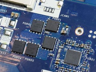
How do you fix a shorted MLCC? Ideally, you replace it with another capacitor of the same value, rating, and form factor. Since these are bypass capacitors, nominal value isn’t critical as it is for feedback components, so replacements only need to be in the general ballpark, preferably higher. Unfortunately, I only have 16V capacitors in stock, and the 25V electrolytic on the other side (along with the 19V coming from the AC adapter) tells me I shouldn’t put a 16V capacitor on there if I don’t want to have unpleasant surprises in the foreseeable future.
The other option is to simply remove the questionable cap and trust that the remaining capacitors elsewhere on the system rail are sufficient to pick up the slack. In the interest of getting this done quickly, I decided to repeal the bad capacitor until the next time I need to order parts and pad my order with some 25V MLCCs.

After removing the capacitor, I measured resistance across the system rail and the short was gone. I then put the laptop back together, snapped the battery back in, plugged in the AC adapter, and watched the battery charging LED light up. I let the flat battery charge while I cleaned my bench, and then pushed the power button. Surprisingly enough, a single shorted capacitor was all that was preventing the laptop from booting. Less surprising was the horizontal streak of backlight bleed-through across the screen (most visible part circled in red). This is much better than the clusters of dead pixels I expected, though.
New Capacitor
Due to multiple interruptions and distractions, this story sat on the shelf for months. The silver lining is that, in the meantime, I had time to order parts for other repairs, allowing me to purchase the proper SMD capacitors. I decided to go back in one more time to see whether the shorted cap I removed was an important one. If not, I could have simply left its pads unpopulated.


Here are those three capacitors in the cluster of interest: the remaining presumed-good 0805 capacitor with some excess solder on it from previous removal and re-installation on the left, my new 1µF capacitor in the middle, and a tiny original 0201 one to its right. How much difference did it make on system rail noise? Not enough to be obvious at a glance. With some squinting and the knowledge that the vertical scale is 50mV per division, you may be able to discern that the top waveform has about 200mV peak-to-peak of ripple and noise instead of 225mVPP, which is sufficient to correctly conclude that the top waveform must be with the replacement capacitor installed. Looking closely at the fine vertical lines corresponding to switching transients, there also is visibly less high-frequency content. Conclusion? The board would probably have been fine for the remainder of its useful life without this capacitor, which makes the 30 minutes I spent taking the laptop apart and putting it back together only to solder a $0.02 part in feel like a waste of time. Although I already suspected as much when I decided to call it done after removing the shorted capacitors months ago, at least I won’t have this question nagging me in the back of my head anymore.
MORE: Best Gaming Laptops
MORE: Gaming Laptop Previews
MORE: All Laptop Content
Current page: Synchronous Rectification Buck Regulator 101 (And A Cure)
Prev Page On The Hunt Next Page The Patient Returns With Unrelated Complications-
Roland Of Gilead Ha, that was interesting!Reply
At first I thought, 'what the heck is this about?'. Thought the title alone was very random. Anyway, I read the article and it's changed my mind. Not only is it well written, but also informative. I've had maybe, three laptops that I've either thrown away or given away, some with minor issues that I couldn't have been bothered to try and troubleshoot. Screens failing, other unusual behaviour with power issues etc. I guess Ill brush up on some basic engineering skills, and give future dead devices a chance for redemption.
Thanks Daniel, I enjoyed that of a Sunday morning :) -
farberj Nice and informative article, nice to see the logical train of thought that a true problem solver uses.Reply -
Danny Leiva Thanks for the very informative piece! About 6 months ago I repaired my wife's macbook air after there was a spill accident that occurred. With resources online, I figured out and was able to diagnose that the connector on the board with the ribbon cable to LCD had a few pins that had disintegrated. Was able to buy the replacement connector online and, after learning to get much better with tiny-piece soldering, was able to replace the connector successfully! Felt really good!Reply -
AnimeMania The real question is how much information was retrievable from the hard drive. Name, address, phone number, SSN#, (amazon, facebook, twitter and banking access), personal photos (some of a very private nature (nude)), tax returns, emails, etc. What are your legal rights to this information, is it similar to when someone buys one of those abandoned storage lockers contents? Anyone with minimal computer skills could probably remove the hard drive and revue its contents.Reply -
Allen_B Great article, thanks! I've got some electronics knowledge but this is inspiration to learn more. It's such a shame to see electronics end up in the trash, and friends having to shell out for new stuff they didn't really need.Reply -
Daniel Sauvageau Reply20251438 said:Ha, that was interesting!
Thanks Daniel, I enjoyed that of a Sunday morning :)
Glad you liked it!20251813 said:Nice and informative article, nice to see the logical train of thought that a true problem solver uses.
Liquid damage can get pretty nasty when power stays on long enough to let electrolysis eat the pads. Congrats on managing to replace the connector!20251834 said:Thanks for the very informative piece! About 6 months ago I repaired my wife's macbook air after there was a spill accident that occurred.
The HDD is fully operational, whatever information on it that wasn't encrypted would have been easy picking. When my friend told me that I could keep the laptop when I couldn't repair the keyboard, I did a factory reset to get rid of the password instead of poking around for ways to crack it.20251991 said:The real question is how much information was retrievable from the hard drive. -
mikewinddale "support your 'Right to Repair' and similar bills"Reply
But that just means that devices will be more expensive. Presumably, devices are being constructed with more proprietary parts that are difficult to repair, because this makes the final product less expensive for the consumer. (After all, manufacturers compete with each other, and it is difficult to imagine them deliberately making their products more expensive than necessary.)
Furthermore, as standards-of-living increase, wages tend to increase relative to raw material and other manufacturing costs. This rise in relative wages means that it is economically less sensible to repair broken devices. When wages are low and manufacturing costs are high, it makes sense to pay a repairman to avoid purchasing a replacement. But when wages are high and manufacturing costs are low, it makes more sense to trash the device and buy a new one.
So a "right to repair" would essentially mean increasing manufacturing costs without any benefit. The device would cost more to purchase, and in the end, high labor costs mean it wouldn't be worth it to repair it anyway, so you'd still end up buying a new device when it breaks. So you're paying more to purchase a repairable device, and even then, it still isn't worth it to repair. -
IInuyasha74 Certainly was an interesting read. Must feel like a big waste of time for a beat up old laptop with an AMD E2 processor in it, but excellent for the fun of seeing a notebook taken apart and parts soldered on and off of it.Reply
Most Popular


