AMD unveiled its next-gen Instinct MI300 accelerator at CES 2023, and we were lucky enough to get some hands-on time and snap a few close-up images of the mammoth chip.
Make no mistake, the Instinct MI300 is a game-changing design - the data center APU blends a total of 13 chiplets, many of them 3D-stacked, to create a chip with twenty-four Zen 4 CPU cores fused with a CDNA 3 graphics engine and 8 stacks of HBM3. Overall the chip weighs in with 146 billion transistors, making it the largest chip AMD has pressed into production.

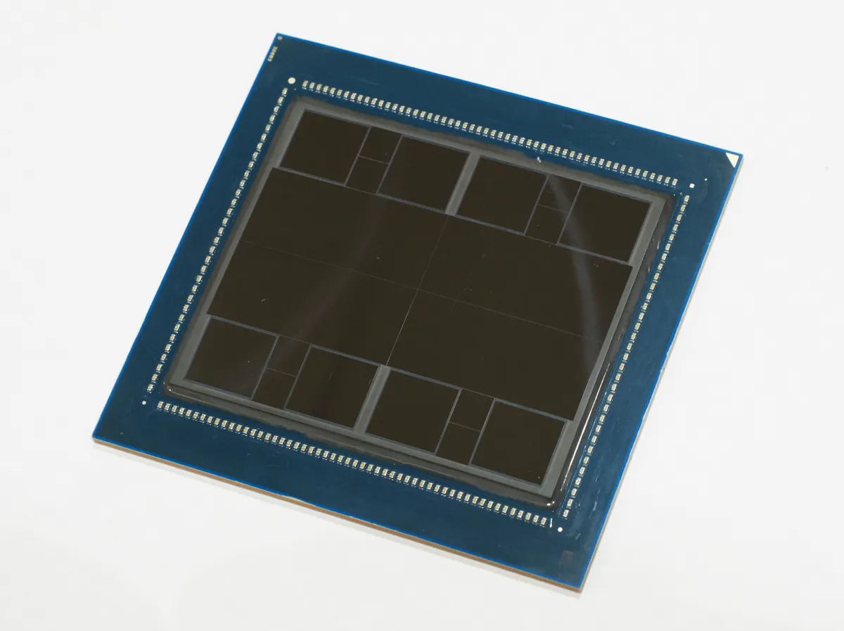
The MI300 weighs in with 146 billion total transistors, easily outweighing Intel's 100 billion transistor Ponte Vecchio, tied together with 128GB of HBM3 memory. The delidded chip is incredibly hard to photograph given its shiny exterior, but you can clearly see the eight stacks of HBM3 that flank the center dies. Small slivers of structural silicon are placed between these HBM stacks to ensure stability when a cooling solution is torqued down atop the package.
The computing portion of the chip consists of nine 5nm chiplets that are either CPU or GPU cores, but AMD hasn't given us details on how many of each are employed. Zen 4 cores are typically deployed as eight-core dies, so we could be looking at three CPU dies and six GPU dies. The GPU dies use AMD's CDNA 3 architecture, the third revision of AMD's data center-specific graphics architecture. AMD hasn't specified the CU count.
Those nine dies are 3D-stacked atop four 6nm base dies that are not merely passive interposers - we're told these dies are active and handle I/O and various other functions. AMD representatives showed us another MI300 sample that had the top dies sanded off with a belt sander to reveal the architecture of the four active interposer dies. There we could clearly see the structures that enable communication not only between the I/O tiles, but also the memory controllers that interface with the HBM3 stacks. We were not allowed to photograph this second sample.
The 3D design allows for incredible data throughput between the CPU, GPU and memory dies while also allowing the CPU and GPU to work on the same data in memory simultaneously (zero-copy), which saves power, boosts performance, and simplifies programming. It will be interesting to see if this device can be used without standard DRAM, as we see with Intel's Xeon Max CPUs that also employ on-package HBM.
AMD's representatives were coy with details, so it isn't clear if AMD uses a standard TSV approach to fuse the upper and lower dies together, or if it uses a more advanced hybrid bonding approach. We're told AMD will share more details about the packaging soon.
AMD claims the MI300 delivers eight times the AI performance and five times the performance per watt than the Instinct MI250 (measured with FP8 with sparsity). AMD also says that it can reduce the training time for ultra-large AI models, like ChatGPT and DALL-E, from months to weeks, thus saving millions of dollars of electricity.
The current-gen Instinct MI250 powers the Frontier supercomputer, the world's first exascale machine, and the Instinct MI300 will power the forthcoming two exaflop El Capitan supercomputer. AMD tells us these halo MI300 chips will be expensive and relatively rare -- these are not a high-volume product, so they won't see wide deployment like the EPYC Genoa data center CPUs. However, the tech will filter down to multiple variants in different form factors.
This chip will also vie with Nvidia's Grace Hopper Superchip, which is the combination of a Hopper GPU and the Grace CPU on the same board. These chips are expected to arrive this year. The Neoverse-based Grace CPUs support the Arm v9 instruction set and systems come with two chips fused together with Nvidia's newly branded NVLink-C2C interconnect tech. AMD's approach is designed to offer superior throughput and energy efficiency, as combining these devices into a single package typically enables higher throughput between the units than when connecting to two separate devices.
The MI300 will also compete with Intel's Falcon Shores, a chip that will feature a varying number of compute tiles with x86 cores, GPU cores, and memory in a dizzying number of possible configurations, but those aren't slated to arrive until 2024.

Here we can see the bottom of the MI300 package with the contact pads used for an LGA mounting system. AMD didn't share details about the socketing mechanism, but we'll be sure to learn more soon -- the chip is currently in AMD's labs, and the company expects to deliver the Instinct MI300 in the second half of 2023. The El Capitan supercomputer will be the world's fastest supercomputer when it is deployed in 2023. It is currently on schedule.


