Intel HPC Roadmap: 800W Rialto Bridge GPU, Falcon Shores XPU, Ponte Vecchio with HBM Benchmarks
Intel broadens its supercomputing playbook on the way to Zettascale
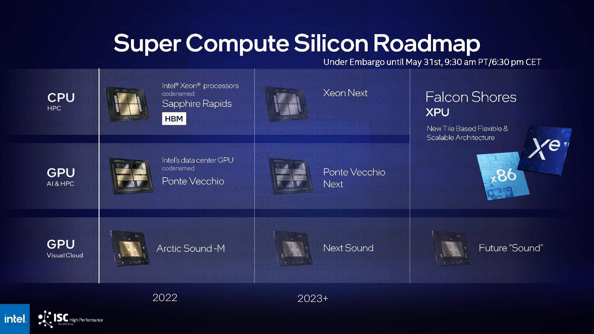
Intel's keynote at the International Supercomputing Conference came with a new roadmap as it works towards its daunting goal of delivering Zettascale-class performance by 2027. As you can see in Intel's Super Compute Silicon Roadmap above, today's announcements include the first details of Intel's Rialto Bridge GPUs, the next generation of its yet-to-be-launched Ponte Vecchio GPUs. The Rialto Bridge data center GPUs will sport up to 160 cores fabbed on a newer process node, come with an obviously heavily-reworked architecture, operate at up to 800W, deliver up to 30% more performance in applications, and begin sampling in mid-2023.
Additionally, Intel shared more details about the Falcon Shores XPU, a chip that will feature a varying number of compute tiles with x86 cores, GPU cores, and memory in a dizzying number of possible configurations. Intel plans to combine its CPU and GPU product lines into this singular composable product, merging the two lineups into one in 2024.
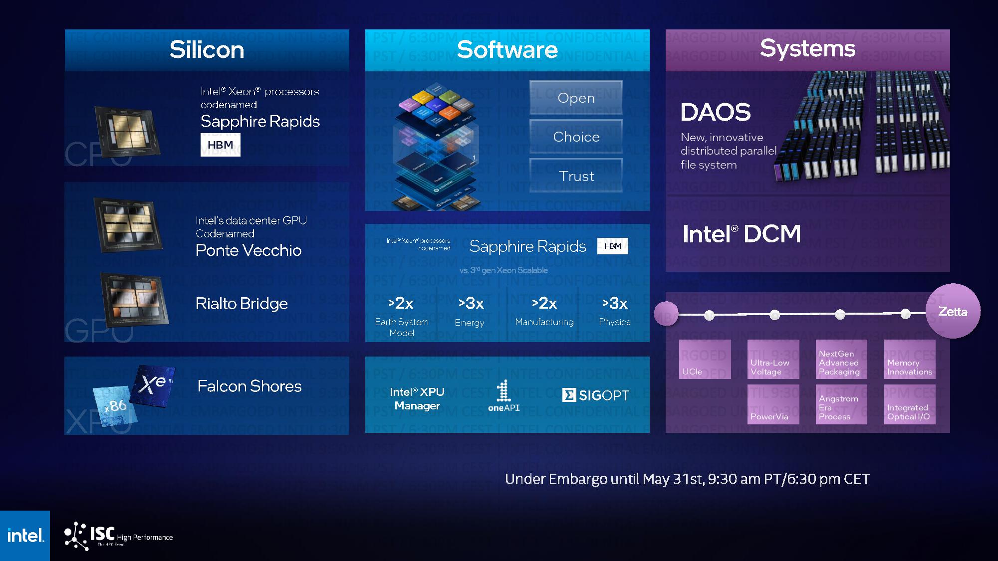
We now also have the first benchmarks of Intel's HBM-equipped Sapphire Rapids server chips working their way to market to contend with AMD's Milan-X processors. Intel claims these chips offer up to three times the performance of their Ice Lake Xeon predecessors in memory throughput-limited applications.
Delivering on Intel's Zettascale goal will require a series of advancements, many of them revolutionary, and today the company also shared some of its nearer-term goals while also sketching out the broader long-term plan with a Zettascale building blocks roadmap. Let's dive into the announcements.
Intel Rialto Bridge GPU and XPU Manager
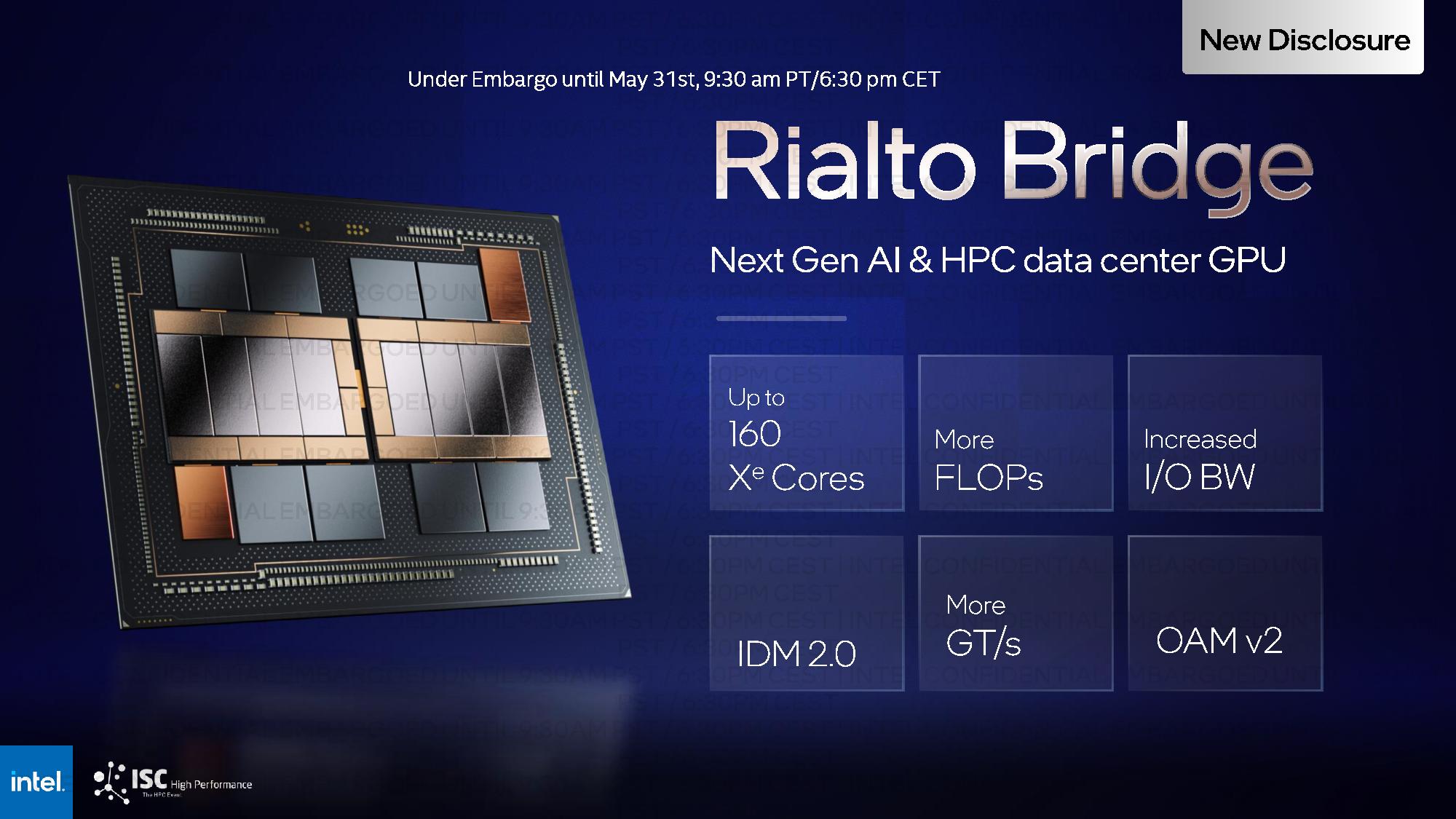
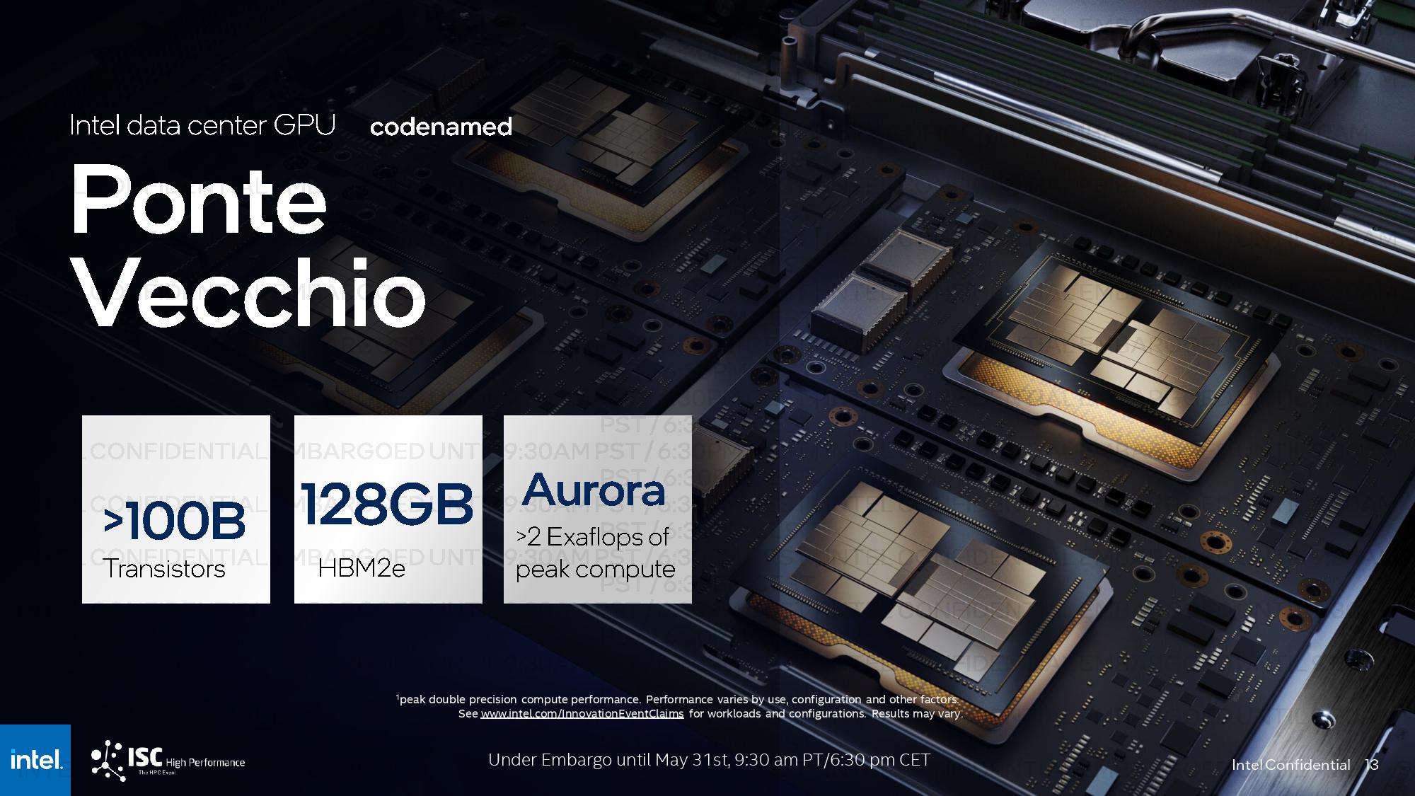

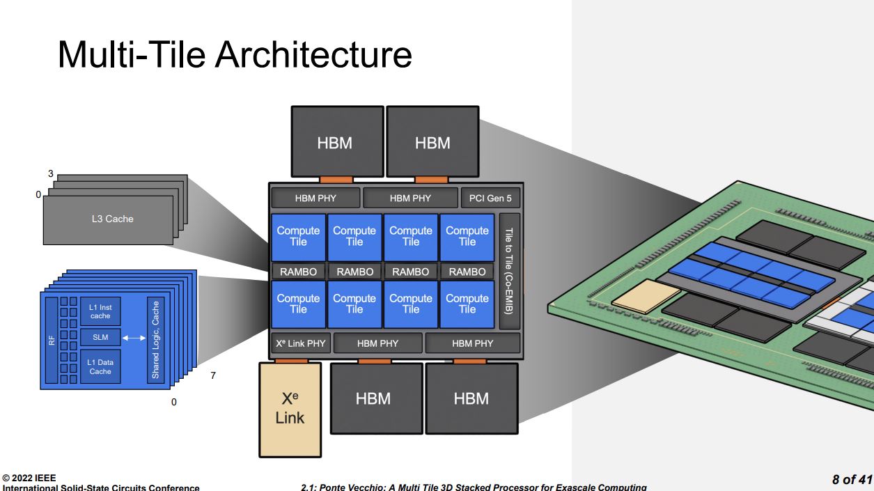
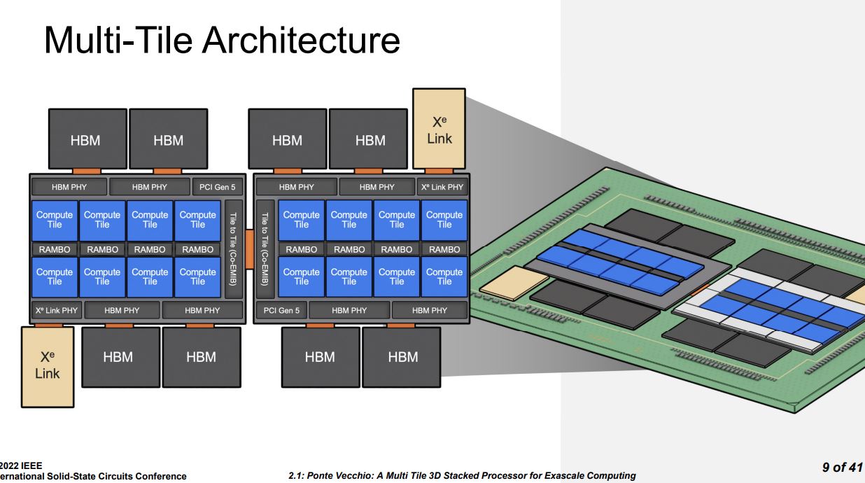
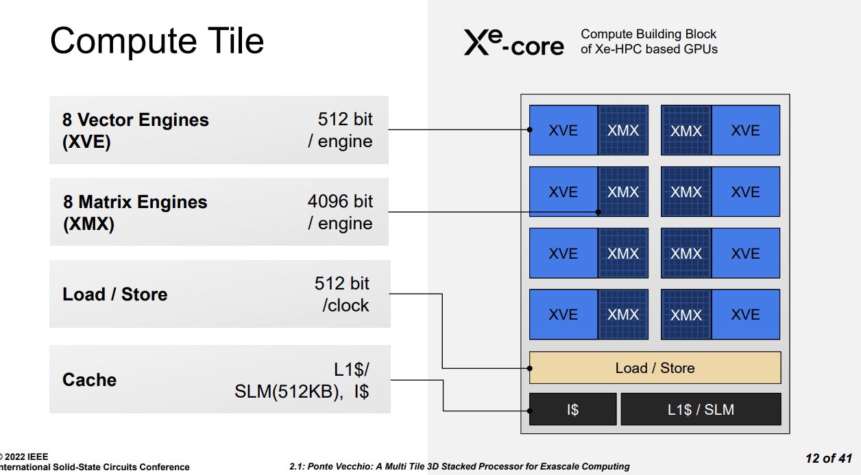
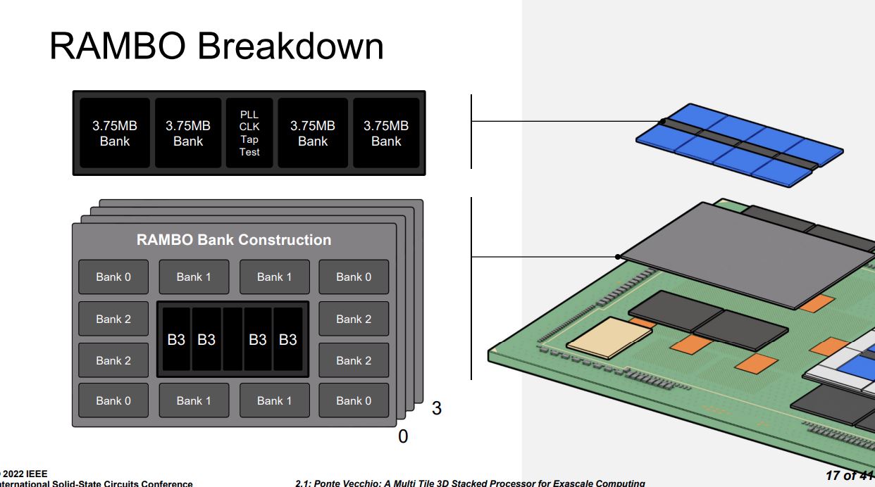
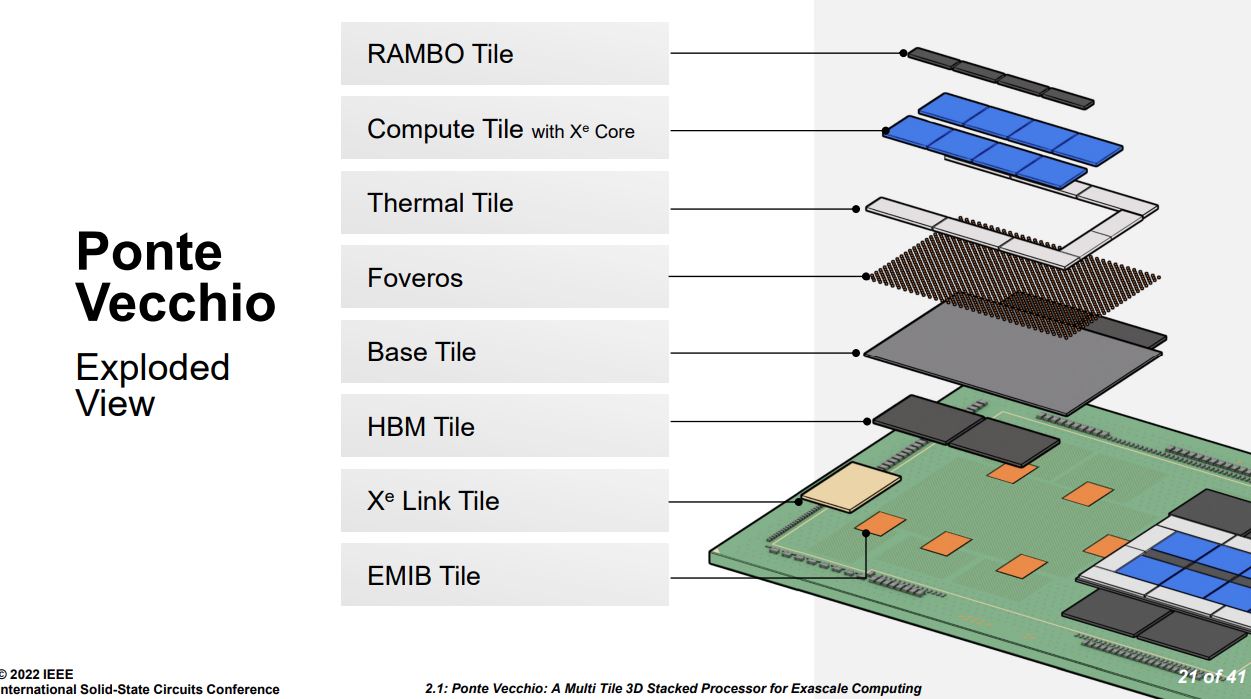
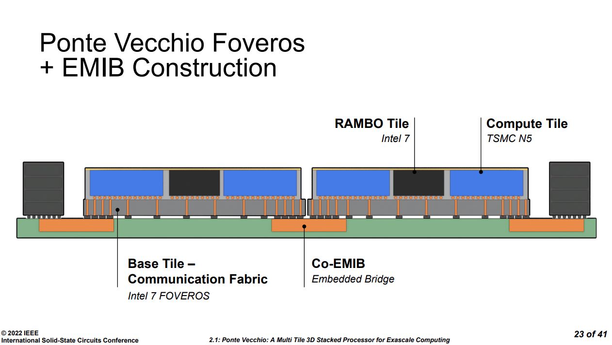
Intel is sticking with naming its enterprise-class GPUs after Italian bridges, with the current-gen Ponte Vecchio followed by Rialto Bridge, Intel's next-gen data center GPU that will come to market in 2023. Intel divulged that this chip would feature up to 160 Xe cores, a substantial increase over the 128 cores present on Ponte Vecchio.
As we can see above, while the Ponte Vecchio design consisted of 16 total compute tiles arranged in two banks that run down the center of the chip, with eight cores per tile, Rialto Bridge only has eight longer tiles with (presumably) 20 Xe cores apiece, signifying a significant design shift.
We also see that Ponte Vecchio's Rambo Cache tiles have been removed, though there are still eight HBM tiles of an unknown flavor flanking the cores while two Xe Link tiles are arranged at opposing corners of the chip package. To help illustrate the differences, the final six images in the above album include block diagrams of the current-gen Ponte Vecchio design.
Rialto Bridge comes with a newer unspecified process node, but Intel hasn't specified which components will get upgrades (presumably, all will move to newer nodes). Currently, Intel uses its 'Intel 7' node for Ponte Vecchio's base tile and cache, TSMC 5nm for the compute tile, and TSMC 7nm for the Xe Link tile.
Rialto Bridge also comes with unspecified architectural enhancements, similar to a "tick,' that confer up to a 30% performance improvement in applications over Ponte Vecchio. Intel hasn't provided any benchmarks to back up those claims yet and we aren't sure if those improvements are at the same clocks/power envelope. However, the 30% projection closely tracks the 25% increase in core count, implying we're not going to see substantial IPC improvements.
Intel lists Rialto Bridge's peak power consumption at 800W, an increase over Ponte Vecchio's 600W peak, and will be available in the Open Accelerator Module (OAM) form factor. Intel says it will adopt the OAM 2.0 spec, though it will also continue to offer its GPUs in other form factors. Rialto Bridge will be compatible with Ponte Vecchio packaging, so it can be a drop-in upgrade.
In addition, the company will soon launch its XPU Manager, an open-source monitoring and management software for its data center GPUs that can be used both locally and remotely. Otherwise, Intel only shared hazy details about this new GPU, using claims like 'more FLOPs,' 'increased I/O bandwidth,' and 'More GT/s' that don't give us any insight into the new design. However, the company did include an IDM 2.0 listing in the slide, indicating that it will continue to use foundry partners for some of the Rialto Bridge tiles. We're sure to learn more soon, though — Intel says Rialto Bridge will arrive in 2023.
Intel Falcon Shores XPU
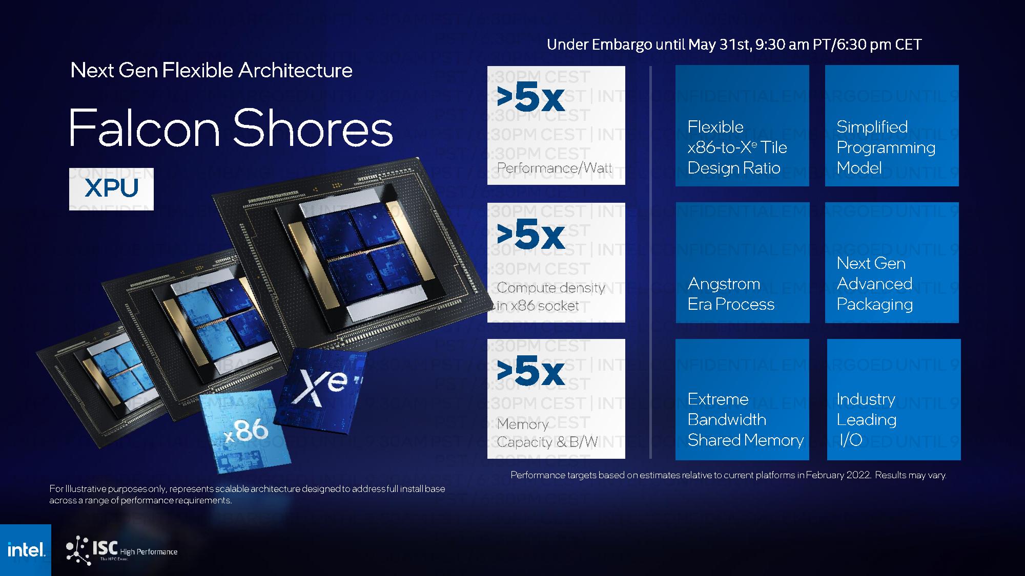
Intel's Falcon Shores XPU represents the continuation of the company's heterogeneous architecture design arc with the end goal of delivering 5X the performance per watt, 5X the compute density in an x86 socket, and 5X the memory capacity and bandwidth of existing server chips. Intel's roadmap of both CPUs and GPUs converges with Falcon Shores, indicating these chips will serve both roles in the future. That's an incredible gamble, but Intel has been building the technological foundation for this sort of paradigm shift for several years, so it has the tools.
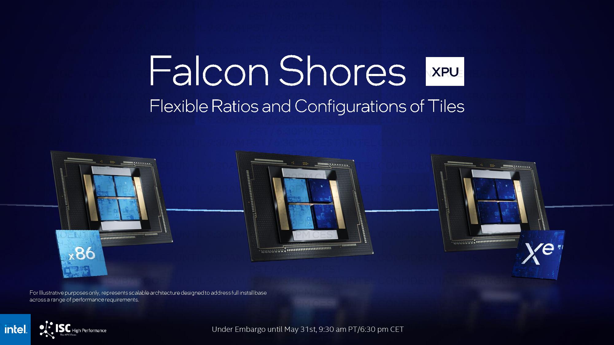
This disaggregated chip design will have separate tiles of x86 compute and GPU cores, but Intel can use those tiles to create any mixture of the two additives, like an all-CPU model, an all-GPU model, or a mixed ratio of the two. Intel hasn't specified, but it is also feasible to expect that the x86 core tiles could have their own mixture of Performance cores (P-cores) and Efficiency cores (E-cores), or we could see clusters of P- and E-cores deployed as complete tiles of their own. Intel notes that these tiles will be fabbed on an unspecified Angstrom-era process node, though Intel's 20A seems to fit the bill for the tiles it could fab itself.
Falcon Shores will come armed with smaller tiles for various flavors of HBM memory and networking additives. The flexible ratio of CPU, GPU, memory, and networking functionality will allow Intel to quickly adjust its Falcon Shores SKUs late in the design process for specific or emerging workloads, an important consideration due to the rapidly-shifting landscape in the AI/ML space. Intel hasn't specified whether or not it will allow customers to mix and match to create their own preferred mixture of tiles, but this would fit well with the company's Intel Foundry Services (IFS) approach that will see it license its own IP and also fabricate chips for other firms. It also isn't hard to imagine other types of tiles, like FPGA or ASIC, working their way into the design if the money is right.
The second slide in the above album shows various combinations of a four-tile design with x86 compute cores and Xe GPU cores, along with four smaller tiles that presumably hold memory and networking chips.
Naturally, this design will allow Intel to leverage its IDM 2.0 model, thus producing some of its own tiles for certain functions while also contracting with third-party fabs and IP providers for some tiles in a mix-and-match fashion that could sidestep any potential fabrication issues with either its own Angstrom-class process node tech, or that of its suppliers. Additionally, leveraging the UCIe ecosystem of chiplets here could prove to be a cornerstone that allows Intel to access the best memory and networking additives the industry has to offer.
Intel will leverage next-gen advanced packaging to deliver 'extreme' bandwidth between the tiles that it will fuse into one cohesive unit. However, it is unclear if these chips will have an (active?) interposer underneath, much as we see with the 3D-stacked Foveros chips, or which flavors of Intel's vast palette of interconnect tech it will use to connect the tiles. Intel has invested heavily in packaging tech, and hopes it pays off here.
Falcon Shores will have a simplified programming model that Intel says will create a "CPU-like" programming experience, presumably based upon the company's OneAPI portfolio. Intel expects this product to come to market in the 2024 timeframe.
Intel Sapphire Rapids HBM Benchmarks
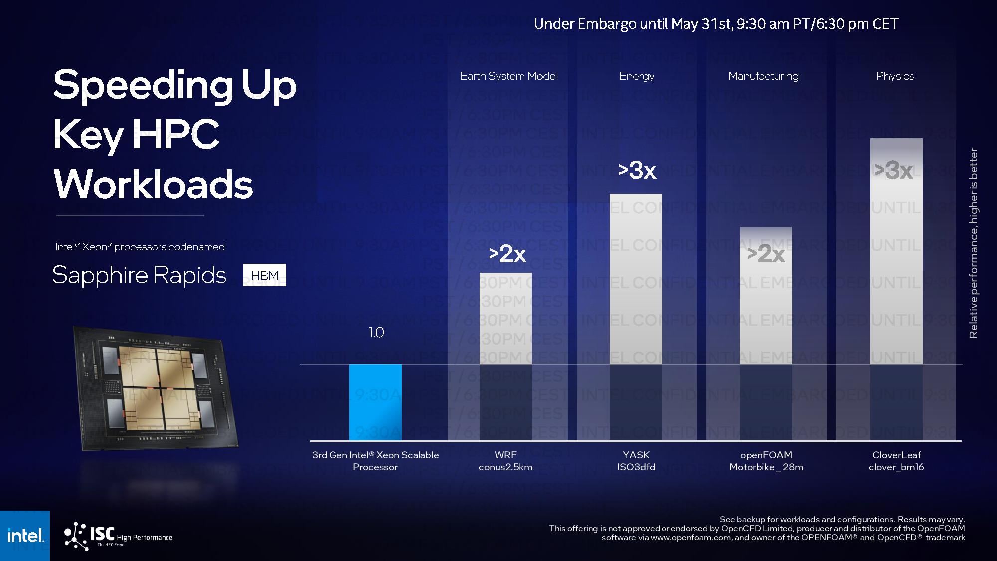
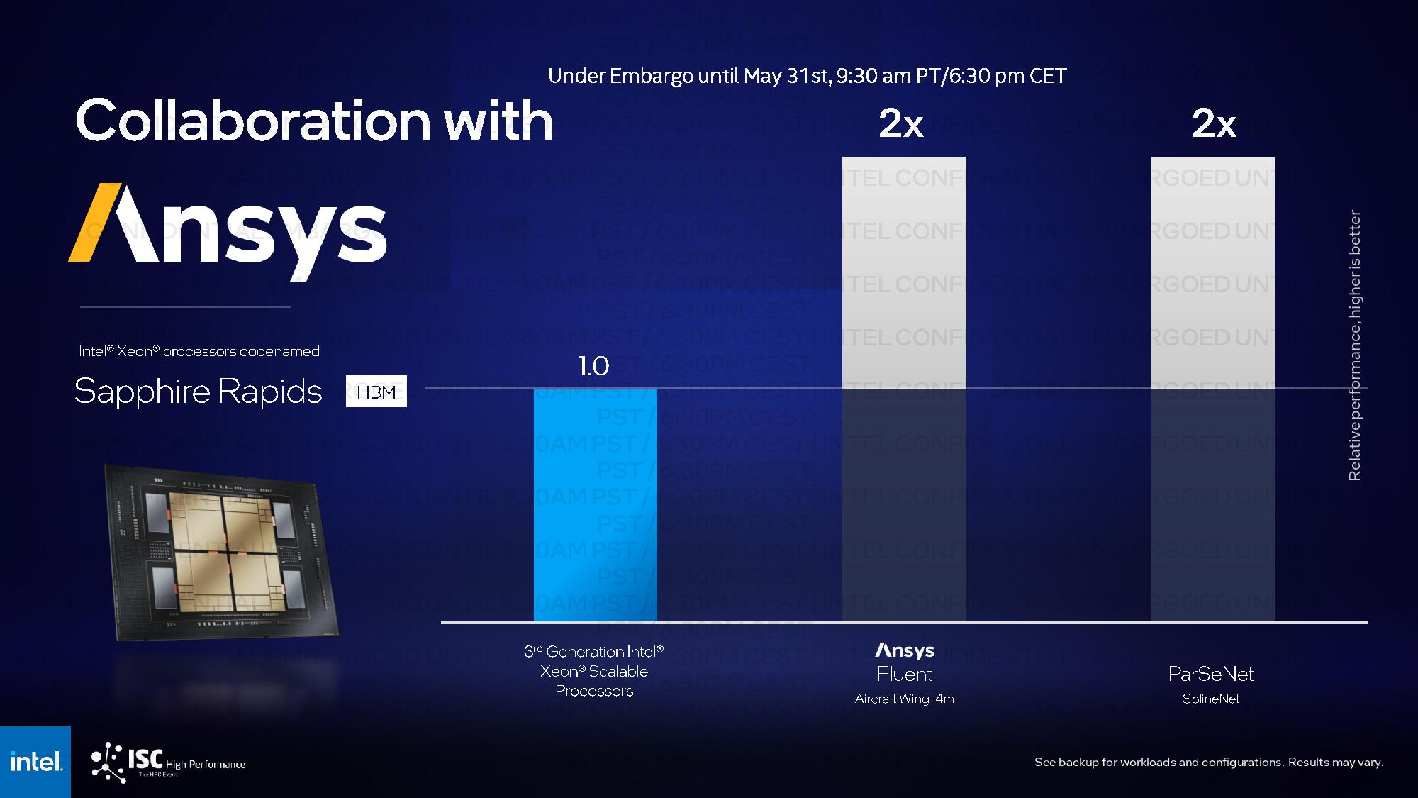
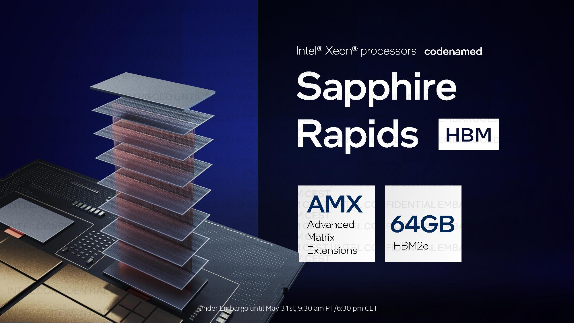
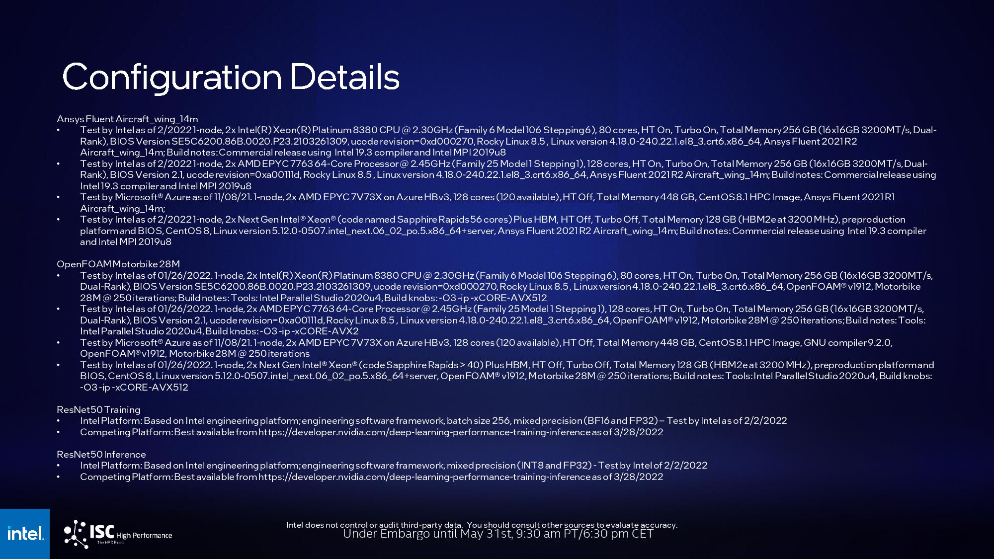
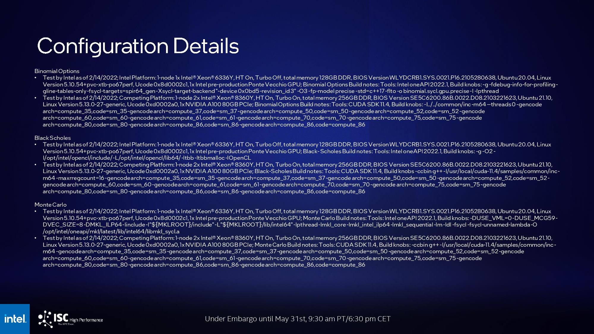
Intel shared benchmarks for its HBM2-equipped fourth-gen Sapphire Rapids Xeon processors, which we know come with up to 64GB of HBM2e memory to boost performance in memory throughput-constrained workloads. As with all vendor-provided benchmarks, take these with plenty of salt. We've included the test notes at the end of the above album.
Intel claims a >2X performance gain over its own Ice Lake Xeon 8380 chip in WRF, a weather forecasting model benchmark that Nvidia recently used to tout its Grace CPU's gains over Intel.
Other highlights include a claimed >3X improvement in the YASK energy benchmark, a 2X improvement in OpenFOAM, and a >3X improvement in the CloverLeaf Euler solver. Intel also claims a 2X speedup in Ansys' Fluent software and a 2X improvement in ParSeNet.
Intel says that its HBM-equipped Sapphire Rapids comes to market this year. The standard Sapphie Rapids models haven't hit the general market yet, so this could be dicey.
Intel's Zettascale Building Blocks
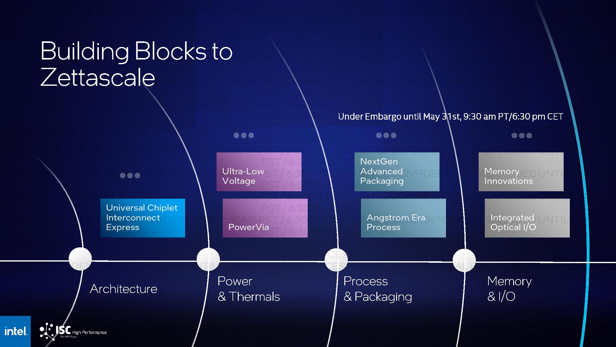
Intel's quest to push forward from the just-minted Exascale era to the Zettascale era is fraught with challenges given its ambitious 2027 goal, particularly as the company has yet to launch its own exascale-class Aurora supercomputer. For now, the exascale crown is AMD's alone with the Frontier supercomputer. Moving to Zettascale will require a 1000X increase in performance and new process node tech, architectures, memories, and packaging technology, not to mention networking technology that ties it all together.
Intel laid out some of the advancements it feels are needed to reach this next level of computing, with the Universal Chiplet Interconnect Express (UCIe) spec being chief among them. UCIe aims to standardize die-to-die interconnects between chiplets with an open-source design, thus reducing costs and fostering a broader ecosystem of validated chiplets. In addition, the UCIe standard aims to be just as ubiquitous and universal as other connectivity standards, like USB, PCIe, and NVMe, while providing exceptional power and performance metrics for chiplet connections. This interconnect allows Intel to access the best IP the industry has to offer, be that in networking, memory, or other additives.
Some future supercomputers may require modular nuclear reactors to feed their expansive appetites for power, so saying that power consumption is a concern is a massive understatement. Intel also plans to extend its Ultra-Low Voltage tech, pioneered in its Bitcoin-mining Blockscale ASICs to provide a 50% clock load voltage reduction, to cut power consumption drastically. This will cut power consumption in high-performance chips, ultimately reducing thermal load and simplifying cooling. Intel's PowerVia tech, which provides backside power delivery to transistors, is another critical advance.
Intel is exploring new memories to provide higher throughput in a smaller package and envisions optical interconnects being brought onto the package to help deal with bandwidth increases. Optical networking could be used for both chip-to-chip and die-to-die links, not to mention extend out of the box in networking scenarios. Intel's Xe Link could pivot to optical interconnects to improve bandwidth, bandwidth density, and reduce power consumption. All of these factors, and more, will be needed for Intel to meet its goal of delivering Zettascale computing power by 2027.
Get Tom's Hardware's best news and in-depth reviews, straight to your inbox.

Paul Alcorn is the Editor-in-Chief for Tom's Hardware US. He also writes news and reviews on CPUs, storage, and enterprise hardware.
-
JamesJones44 Interesting that the watt usage per core is going up 0.5 watts over last gen with a die shrink, I'm curious to see what frequencies they end up running these at.Reply -
dehjomz This all sounds cool, but the question I always have for Intel is, when will the Silicon ship? I'm looking forward to the innovations and I hope Intel can bring them market sooner rather than later. I'm looking forward to what AMD does with Xilinx and Persando.Reply -
targetdrone Before you know it we'll need a dedicated 240V outlet to run a home gaming computer.Reply -
Kamen Rider Blade Reply
Don't give nVIDIA & Intel anymore ideas. They might take it seriously.targetdrone said:Before you know it we'll need a dedicated 240V outlet to run a home gaming computer. -
escksu ReplyJamesJones44 said:Interesting that the watt usage per core is going up 0.5 watts over last gen with a die shrink, I'm curious to see what frequencies they end up running these at.
OK, you have to note that these chips are not intended for consumer user. They are meant for high performance computing (Eg. supercomputers). So, the important thing isn't the how much the chip consume but rather overall performance/watt (eg. Gigaflop per watt).
An example. Say this chip is 100 GFlop and 800W (just an example), older chips are 75GFlop and 600W. Chipwise, both are same performance/watt.... Don't seem that impressive. But here is the catch, to achieve 10,000 GFlop, you need 100 of the new chip instead of 133 of the older ones....
33 more chips means more hardware needed to support these chips. More circuit boards, voltage regulators, interconnects, etc etc.....All additional hardare consume and dissipate power. So cost and power consumption goes up. -
escksu Replytargetdrone said:Before you know it we'll need a dedicated 240V outlet to run a home gaming computer.
ITs not meant for gaming, not meant for consumer use. -
Rdslw Reply
I am quite worried it will be an absurd fireball. I personally would be hesitant to use such power hungry part without long experience in the field. I expect they will have incidents and with that kind of power, it will be intense. (stuff like PCIE data line + 300W power line being single water drop distance from one another like apple did)JamesJones44 said:Interesting that the watt usage per core is going up 0.5 watts over last gen with a die shrink, I'm curious to see what frequencies they end up running these at.
You have 33% less gpu's which means ~33% less racks to worry about. I expect same peta scale supercomputer would end up ~5-10% less power with this and You also have less switching and scheduling, so overall performance can gain a few percents as well.escksu said:OK, you have to note that these chips are not intended for consumer user. They are meant for high performance computing (Eg. supercomputers). So, the important thing isn't the how much the chip consume but rather overall performance/watt (eg. Gigaflop per watt).
An example. Say this chip is 100 GFlop and 800W (just an example), older chips are 75GFlop and 600W. Chipwise, both are same performance/watt.... Don't seem that impressive. But here is the catch, to achieve 10,000 GFlop, you need 100 of the new chip instead of 133 of the older ones....
33 more chips means more hardware needed to support these chips. More circuit boards, voltage regulators, interconnects, etc etc.....All additional hardare consume and dissipate power. So cost and power consumption goes up.
My instincts tell me that something will be wrong, though. I feel like there was a reason why cards were not 1000W each before, and they will have incredible problems with those... -
JamesJones44 Replyescksu said:OK, you have to note that these chips are not intended for consumer user. They are meant for high performance computing (Eg. supercomputers). So, the important thing isn't the how much the chip consume but rather overall performance/watt (eg. Gigaflop per watt).
An example. Say this chip is 100 GFlop and 800W (just an example), older chips are 75GFlop and 600W. Chipwise, both are same performance/watt.... Don't seem that impressive. But here is the catch, to achieve 10,000 GFlop, you need 100 of the new chip instead of 133 of the older ones....
33 more chips means more hardware needed to support these chips. More circuit boards, voltage regulators, interconnects, etc etc.....All additional hardare consume and dissipate power. So cost and power consumption goes up.
Yes, I understand they are not for consumers. My point was, this CPU seems to use 0.5 watts per core more than its predecessor, I'm curious as to why that would be given the die shrink. My thought was maybe they are running them at much higher clocks, but that could be wrong. My primary curiosity is what the PPW ends up being if they are running at very high clock speeds. -
escksu ReplyJamesJones44 said:Yes, I understand they are not for consumers. My point was, this CPU seems to use 0.5 watts per core more than its predecessor, I'm curious as to why that would be given the die shrink. My thought was maybe they are running them at much higher clocks, but that could be wrong. My primary curiosity is what the PPW ends up being if they are running at very high clock speeds.
I am not sure as they did not give more details on the cores. However, it could be numerous factors, so its hard to tell. Can be more cache, more executions units etc etc. Like you said, can be clockspeed too.