ARM Pitches Tri-gate Transistors for 20nm and Beyond
ARM could be introducing Fin-Shaped Field Effect Transistors (FinFET) in 20 nm and smaller chip designs.
Get Tom's Hardware's best news and in-depth reviews, straight to your inbox.
You are now subscribed
Your newsletter sign-up was successful
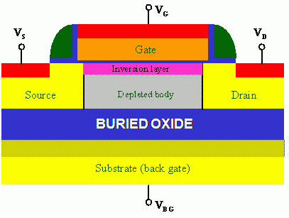
According to a blog post by Jean Luc Pelloie, the company's Fellow Director of SOI Technology, 20 nm may represent an inflection point in which it will be necessary to transition from a metal-oxide semiconductor field-effect transistor (MOSFET) to Fin-Shaped Field Effect Transistors (FinFET) or 3D transistors, which Intel refers to as tri-gate designs that are set to debut with the company's 22 nm Ivy Bridge product generation.
Pelloie explains that it is "increasingly difficult to control the vertical electric field between the gate and the substrate while maintaining the channel depletion below threshold and then minimize the leakage current" when shrinking transistors. FinFETs are considered a solution to solve this problem. The engineer wrote that FiNFETs could be used on either bulk or SOI wafers. However, ARM still has work to do and especially investigate the scalability of this technology. "However, 3D devices are clearly on the road for sub-20nm nodes … and FinFET’s time may finally be here," Pelloie wrote.
FinFET history goes back to a December 2000 paper published in IEEE Transactions on Electron Devices entitled "FinFET - A Self-Aligned Double Gate MOSFET Scalable to 20 nm". Intel was first to move to tri-gates and take this technology into mass-production, but was accused of having switched to 3D transistors only because it was not able to scale its SRAMs, which the company traditionally uses to unveil a manufacturing process, from 32 nm to 22 nm. Intel's tri-gate technology was announced back in May of this year. Intel hopes that tri-gate technology will keep up with Moore's Law and especially drive low-voltage and low-power features.
Article continues belowGet Tom's Hardware's best news and in-depth reviews, straight to your inbox.

Wolfgang Gruener is an experienced professional in digital strategy and content, specializing in web strategy, content architecture, user experience, and applying AI in content operations within the insurtech industry. His previous roles include Director, Digital Strategy and Content Experience at American Eagle, Managing Editor at TG Daily, and contributing to publications like Tom's Guide and Tom's Hardware.
-
freggo Don't you just wish you could take a peek at the computer news in say the year 2212?Reply
We are all quick to dismiss this CPU and that storage device as too slow, too expensive and too whatever. But we have come a long way from the ZX-81 and C64 in a relatively short period of time.
So, given a 200 year time span, what will we be dealing with, and still dismissing as too slow, expensive and what have you.
I wish time travel was more affordable so I could have a look :-)
-
vigilante212 If we could look 200 years into the future I don't think we would even understand what we were looking at concerning computers.Reply -
jujuvivi Sooner or later, silicon transistor technology will reach its limit, slow down and stop.Reply
It might happen in the next 50 years or less.
This doesn't mean we won't produce chips any more,
but that their quality will be more or less the same:
certainly not twice smaller and faster every 3 years.
Mass production of chips based on a completely different techno are still science fiction today. -
CaedenV My bet is that in 2212 we would no longer have traditional 'computers' any longer, and that we would have moved to embedded machines (or something completely else) by that point. Hope I get to see it :)Reply
@jujuvivi
I think we will hit the wall in 20-25 years before moving on so some other type of computing technology (they are talking about hitting the 8-10nm wall within 10 years). After that it will become about 3D chip design (stacked/layered chips), better design, more efficient software, and moving on to quantum computing or some other technology yet to be invented.
What I think is really crazy/wierd about technology is that my son will likely never have a traditional desktop of his own (or at least not need to), and that kids who are currently computer illiterate will never need to become literate because everything will move to personal sized devices using server/cloud services where all that matters is bandwidth and screen size/quality.
The future is wierd, but it is neat to see where ARM and x86 take us. -
itpro Well, if you believe the prognosticators, in 200 years humans will no longer exist and the planet will be populated by intelligent machines. If we do still exist, we will be slaves to our digital overlords, existing only to service the collective.Reply -
BSMonitor ksampannaYes, that is great & all, but first let's survive the 2012 holocaustReply
Crap, what did you hear?? Are we going to elect another brain dead pot fiend Republican as President... Again... -
Namey BSMonitorCrap, what did you hear?? Are we going to elect another brain dead pot fiend Republican as President... Again...Reply
We've already had crackhead and snake in the grass/false hope prezies. I think pot is the least of our worries. -
daneren2005 itproWell, if you believe the prognosticators, in 200 years humans will no longer exist and the planet will be populated by intelligent machines. If we do still exist, we will be slaves to our digital overlords, existing only to service the collective.I never understood why people think superior robots that can mass produce 100x more efficient robots than ourselves would ever have any interest in enslaving mankind.Reply -
stingstang daneren2005I never understood why people think superior robots that can mass produce 100x more efficient robots than ourselves would ever have any interest in enslaving mankind.You are correct. It would require too many resources to keep us alive. Yes sir, our kind will all be in the ground by then.Reply
