China's YMTC Starts Production of 128-Layer, 3D QLC NAND
Planing to serve China's need for NAND, and then some

Get Tom's Hardware's best news and in-depth reviews, straight to your inbox.
You are now subscribed
Your newsletter sign-up was successful
Yangtze Memory Technologies (YMTC) is reportedly now shipping 128-layer, QLC-based consumer-grade NAND manufactured with the company's in-house 3D Xtacking technology. The move is seen as an important one for China to reduce its dependence on high-tech and semiconductor imports, and the company is beginning market penetration via consumer-geared solutions that will be employed in Chinese smartphones and notebooks.
The aim is to take advantage of the explosive growth in capacity requirements for storage applications, as well as for emerging and ballooning technologies such as 5G.
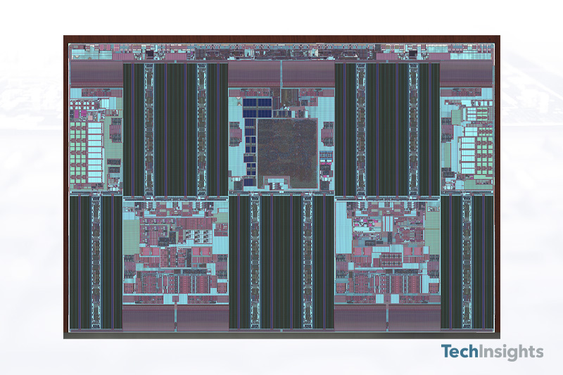
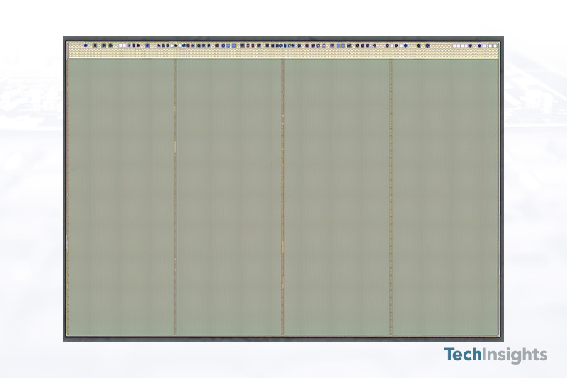
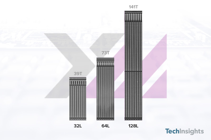
Tech Insights did a teardown of Asgard's latest PCIe 4.0, AN4 1TB SSD solution, which is the first commercial application of the 128-layer manufacturing technology. According to YMTC COO Cheng Weihua, this is a result of volume production being achieved on the 128-layer design. For now, the company's Xtacking 2.0 tech is being used in the manufacturing of 128-layer 512Gb TLC dies (TLC being the preferred cell information density from YMTC until now), as well as the 128-layer QLC 3D NAND itself. The company plans to transition to its Xstacking 3.0 design sometime in the latter half of 2022, with production capacity reaching its peak output by then.
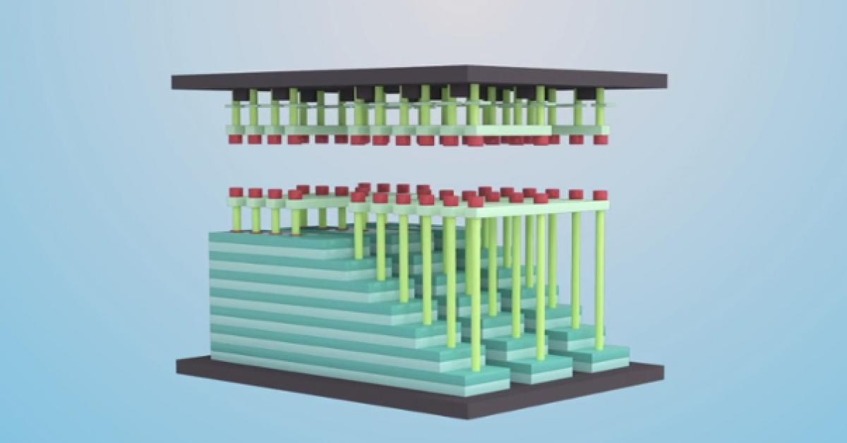
Article continues belowYMTC's Xstacking 2.0 is a 3D manufacturing technology that shies away from actual 3D manufacturing. Instead, the NAND flash's expansion in the Z axis is done via bonding two separately-manufactured wafers: One of these deals with the actual NAND array itself, while the other holds the CMOS circuitry (such as page buffers, column decoders, charge pumps, global datapath and voltage generators/selectors).


The Xstacking technology behind the manufacturing process has been well-received by the industry. The company achieved a 92% higher bit density (8.48 Gb/mm2, 512 Gb) compared to dies manufactured with xStacking 1.0 (4.42 Gb/mm2, 256 Gb), showing that YMTC has a robust future plan for the technology's roadmap. Perhaps more surprising is that YMTC has achieved higher levels of density (8.48) with its TLC Xtacking 2.0 NAND than Samsung (6.91), Micron (7.76) and Sk hynix (8.13). A welcome reversal of expectations for Chinese tech, then; however, YMTC did bring its 128-layer process later to market than the aforementioned manufacturers - there was more knowledge and design time accumulated for their solution than for any of the others.
The launch comes on the heels of a reported delay on volume manufacturing capabilities for the 128-layer QLC NAND, with the company citing unsatisfactory yields as the deciding factor in pushing volume production forward. It's currently unclear if the company has already surpassed those difficulties and is now on schedule with its 100,000 WPM (wafer starts per month); however, the presence of the company's latest NAND in consumer-geared solutions only, sacrificing the high-revenue of professional and server-bound applications, does point towards a conservative estimate on the company's advances when it comes to yields.
Get Tom's Hardware's best news and in-depth reviews, straight to your inbox.

Francisco Pires is a freelance news writer for Tom's Hardware with a soft side for quantum computing.