Researchers See Twinkle of Promise in Diamond Transistors
It is all about improved electron hole mobility.

The unique properties of carbon, when in diamond form, have long drawn the interest of semiconductor researchers. Though heralding diamonds as the next big thing in semiconductors has seen many false starts (and non-starts), some new research from Japan offers renewed promise.
The critical advance demonstrated by researchers from Japan’s National Institute for Materials Science (NIMS) is the design of a diamond field-effect transistor (FET) with high electron hole mobility. Greater hole mobility is desirable because it reduces conduction losses and allows higher operational speeds. However, previous researchers decimated this inherent quality of diamond in their efforts to induce electrical conductivity, which is essential for electronic functionality.
For reference, 'electron hole mobility' is often shortened to just 'hole mobility'. Electrons move in semiconductor crystal lattices, pulled by an electromagnetic field, and so do holes – the positions where the electron can reside. When an electron is excited into a higher state, it leaves a hole in its old state.
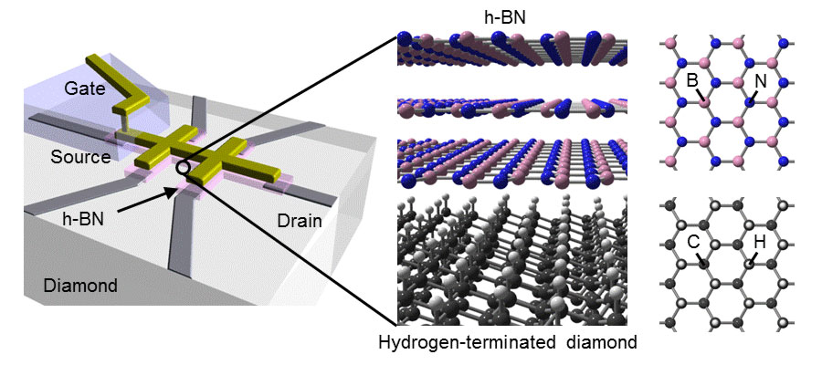
The NIMS researchers, led by principal researcher Takahide Yamaguchi, demonstrated promising results from their new diamond FET, but how did they make it? In the diagram below/left, you can see the structure and materials used to make the breakthrough transistor. Below/right, you can see a micrograph of the diamond FET fabricated by NIMS.
Article continues belowNIMS used single-crystalline hexagonal boron nitride (h-BN) instead of typical oxide material for the gate insulator. There is a graphite gate electrode, and diamond is the substrate. Additionally, the researchers fabricated the new FET in argon gas and then laminated it in h-BN, so it didn't have any contact with air.
Previous attempts at making diamond transistors faced the problem of "very low mobility of between just 1 to 10% of diamond's original hole mobility," according to Yamaguchi. In years past, FET research used diamonds with their superficial carbon atoms covalently bonded with hydrogen atoms. This hydrogen doping technique was previously thought necessary for electrical conductivity but actually stood in the way of diamond's natural wide bandgap semiconductor properties. Unfortunately, this introduced carrier scattering, decimating the material's natural hole mobility.
However, the new diamond FET design offers a "hole mobility five times that of conventional FETs using oxide gate insulators, and more than twenty times that of GaN and SiC p-channel FETs," according to Yamaguchi. Higher hole mobility also means lower conduction loss, so "a twenty-times increase in channel mobility means a one-twentieth reduction loss in the channel," he explained.
Potential First Use Case Applications
The researchers think these new components would be highly desirable in electronics applications where low-loss power conversion and high-speed communications are essential. Another interesting, and potentially very useful, quality of diamond FETS is that they have a normally-off characteristic – which is of great appeal in fail-safe power electronic applications, for example.
Get Tom's Hardware's best news and in-depth reviews, straight to your inbox.
There is still plenty of work needed to refine diamond FETs and make them a practical and useful alternative; however, NIMS has made a significant advance. Even with the obvious obstacle of cost holding back adoption and the issue with the maximum size of diamond wafers blocking the way, some early adopters might still be attracted to diamond FETs.

Mark Tyson is a news editor at Tom's Hardware. He enjoys covering the full breadth of PC tech; from business and semiconductor design to products approaching the edge of reason.
