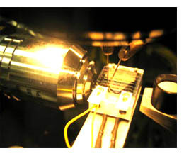
New Intel laser tech could bring photonics to the masses
Get Tom's Hardware's best news and in-depth reviews, straight to your inbox.
You are now subscribed
Your newsletter sign-up was successful
Santa Clara (CA) - Optical components that provide high-bandwidth data transmission today are mostly used in the telecommunications industry and are often too expensive for mainstream technologies. Intel now claims to have found a way to use silicon as optical material - a discovery that could lead to cheaper lasers as well as faster and more capable networks in the future.
Intel calls its "breakthrough" research the "first continuous silicon laser" which allows amplifying photons within silicon material to create a laser output beam. Silicon so far was considered to be unsuited for such an application due to its nature to create strong electromagnetic interference and absorb most of the source light.
"99 percent of the world is still copper," said Dr. Mario Paniccia, Director of Intel's Photonics Technology Lab. Backbone and long data transmission infrastructures with ranges from 300 feet to about 45 miles today are implemented via fiber optics. Rack-to-rack, board-to-board and chip-to-chip connections however are copper-based, mainly because of cost factors. Intel's research results could change this scenario and move high-bandwidth laser technologies down to a chip level.
Paniccia said that the results are just a few weeks old and it was too early to predict, when the technology could be introduced into the mass market. "We created an opportunity that may enable us to combine photonics with common CMOS technology. The future will have to tell how these will work together. It's a matter of cost and integration," he said. The goal however was to transfer the research into commercial products "by the end of the decade".
Potential applications of the silicon laser could include lasers on a chip for telecommunications and networking with high bandwidths: "We think 10 Gbit per second is a start," Paniccia said. Medical devices using high-frequency lasers could become much smaller and cheaper in the future.
The building blocks of Intel's laser consist of the light source, waveguides and light splitter, a modulator, light detection, low-cost assembly and intelligence to combine the technology with CMOS on a chip. All components are currently part of the research program, according to Intel.
What kept the industry to take advantage is the fact that silicon electrons can be knocked out from their atoms through a simultaneous hit by two photons. The result is a cloud of electrons that individually absorb light and cancel the Raman amplification. Intel however found that all electrons could be drawn to one side of the silicon by applying a power source around the silicon. This approach frees the way for photons and allows the creation of a pure laser beam. This laser beam can carry a data beam that matches its wavelength.
Get Tom's Hardware's best news and in-depth reviews, straight to your inbox.
Intel researchers say they are unsure about specific applications this technology could enable but stress it is too early to make any predictions and the announcement just shows a "snapshot" of where the technology could lead to.
The company has a long way to go until networks and communications could take advantage of the research result. So far, the company still has to complete all pieces of its building blocks and work on the efficiency of the silicon laser: According to Paniccia, the announced silicon laser creates an output of eight milliwatts and has an efficiency of about five percent.

Wolfgang Gruener is an experienced professional in digital strategy and content, specializing in web strategy, content architecture, user experience, and applying AI in content operations within the insurtech industry. His previous roles include Director, Digital Strategy and Content Experience at American Eagle, Managing Editor at TG Daily, and contributing to publications like Tom's Guide and Tom's Hardware.
