New research along the frontiers of materials engineering holds promise for a truly astounding performance improvement for computing devices. A research team helmed by Markus Hellbrand et al. and associated with the University of Cambridge believes the new material, based of hafnium oxide layers tunneled by voltage-changing barium spikes, fuses the properties of memory and processing-bound materials. That means the devices could work for data storage, offering anywhere from 10 to 100 times the density of existing storage mediums, or it could be used as a processing unit.
Published in the Science Advances journal, the research gives us a road through which we might end with far greater density, performance and energy efficiency in our computing devices. So much so, in fact, that a typical USB stick based on the technology (which is called continuous range) could hold between 10 and 100 times more information than the ones we currently use.
With RAM doubling in density every four years, as pointed out by JEDEC, it'd take RAM makers decades to eventually achieve the same level of density as this technology has shown today.
The device is also a light at the tunnel of neuromorphic computing. Like the neurons in our brain, the material (known as a resistive switching memory) holds the promise of working as both a storage and processing medium. That's something that simply doesn't happen in our current semiconductor technology: the transistor and materials design arrangements are so different between what you need for a memory cell and what you need for a processing one (mainly in terms of endurance, as in, the ability not to suffer performance degradations) that there's currently no way to merge them.
This inability to merge them means that information must be continuously flowing between the processing system and its various caches (when thinking of a modern CPU), as well as its external memory pool (looking at you, best DDR5 kits on the market). in computing, this is known as von Neumann's bottleneck, meaning that a system with separate memory and processing capabilities will be fundamentally limited by the bandwidth between them both (what's usually known as the bus). This is why all semiconductor design companies (from Intel through AMD, Nvidia, and many others) design dedicated hardware that accelerates this exchange of information, such as Infinity Fabric and NVLink.
The problem is that this exchange of information has an energy cost, and this energy cost is currently limiting the upper bounds of achievable performance. Remember that when energy circulates, there are also inherent losses, which result in increased power consumption (a current hard limit on our hardware designs and a growing priority in semiconductor design) as well as heat — yet another hard limit that's led to the development of increasingly exotic cooling solutions to try and allow Moore's law to limp ahead for a while yet. Of course, there's also the sustainability factor: it's expected that computing will consume as much as 30% of the worldwide energy needs in the not-so-distant future.
“To a large extent, this explosion in energy demands is due to shortcomings of current computer memory technologies,” said first author Dr. Markus Hellenbrand, from Cambridge’s Department of Materials Science and Metallurgy. “In conventional computing, there’s memory on one side and processing on the other, and data is shuffled back between the two, which takes both energy and time.”
The benefits of merging both memory and processing are quite spectacular, as you might imagine. While conventional memory is capable of just two states (one or zero, the cause for the "binary" nomenclature), a resistive switching memory device can change its resistance through a range of states. This allows it to function at increased varieties of voltages, which in turn allows for more information to be encoded. At a high enough level, this is much the same process happening in the NAND realm, with increases in bits per cell corresponding to a higher number of possible voltage states unlocked in the memory cell's design.
One way to differentiate processing from storing is saying that processing means that the information is undergoing writes and rewrites (additions or subtractions, transformations or reorganizations) as fast as its switching cycle is requested to. Storing means that the information needs to be static for a longer period of time — perhaps because it's part of the Windows or Linux kernels, for instance.
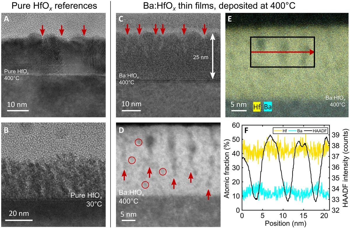
To build these synapse devices, as the paper refers to them, the research team had to find a way to deal with a materials engineering bottleneck known as the uniformity problem. Because hafnium oxide (HfO2) doesn't possess any structure at the atomic level, the hafnium and oxygen atoms that can make or break its insulating properties are deposited haphazardly. This limits its application for conducting electrons (electrical power); the more ordered the atomic structure is, the least resistance will be caused, so the higher the speed and efficiency. But the team found that depositing barium (Ba) within the thin films of unstructured hafnium oxide resulted in highly-ordered barium bridges (or spikes). And because their atoms are more structured, these bridges can better allow the flow of electrons.
But the fun began when the research team found they could dynamically change the height of the barium spikes, allowing for fine-grained control of their electrical conductivity. They found that the spikes could offer switching capabilities at a rate of ~20ns, meaning that they could change their voltage state (and thus hold different information) within that window. They found switching endurances of >10^4 cycles, with a memory window >10. This means that while the material is fast, the maximum number of voltage state changes it can currently withstand stands at around 10,000 cycles - not a terrible result, but not an amazing one.
It's equivalent to the endurance available with MLC (Multi-Level Cell) technology, which will naturally limit its application - the usage of this material as a processing medium (where voltage states are rapidly changed in order to keep a store of calculations and their intermediate results).
Doing some rough napkin math, the ~20 ns switching leads to an operating frequency of 50 MHz (converting to cycles per nanosecond). With the system processing different states at full speed (working as a GPU or CPU, for instance), that means the barium bridges would cease functioning (hit their endurance limit) at around the 0,002-second mark (remember, it's only operating at 50 MHz). That doesn't seem like it could be performant enough for a processing unit.
But for storage? Well, that's where the USB stick that's "10 to 100 times denser" in terms of memory capacity comes in. These synapse devices can access a lot more intermediate voltage states than even the densest NAND technology in today's roomiest USB sticks can - by a factor of 10 or 100.
Who wouldn't love to have a 10 TeraByte or even 100 TeraByte "USB 7" stick on their hands?
There's some work to be done in terms of endurance and switching speed of the barium bridges, but it seems like the design is already an enticing proof of concept. Better yet, the semiconductor industry already works with hafnium oxide, so there are fewer tooling and logistics nightmares to fight through.
But here's a particularly ingenious product possibility: imagine that the technology improves to the point that it's fabricated and useable to design an AMD or Nvidia GPU (which these days operate at around the 2 GHz mark). There's a world where that graphics card comes with a reset factory state where it's entirely operating as memory (now imagine a graphics card with 10 TB of it, the same as our hypothetical USB stick).
Imagine a world where what AMD and Nvidia offered were essentially programmable GPUs, with continuous range-based GPU dies product-stacked in terms of maximum storage capability (remember the 10 to 100 denser than current USB). If you are an AI aficionado attempting to build your own Large Language Model (LLM), you can program your GPU so that just the right amount of these synthetic devices, these neuromorphic transistors, runs processing functions — there's no telling how many trillion parameters models will eventually end up as their complexity increases, so memory will grow increasingly more important.
Being able to dictate whether the transistors in your graphics card are used exactly as memory or exactly as eye-candy-amplifiers to turn graphics settings up to eleven, that'd be entirely up to the end-user; from casual gamer to High Performance Computing (HPC) installer. Even if that meant a measured decay in the longevity of parts of our chip.
We're always upgrading them anyway, aren't we?
But let's not get ahead of ourselves. Even though this isn't as dangerous an issue as AI development and its regulation, there's little to be gained in dreaming so far ahead. Like all technology, it'll come - when it's ready. if it ever is.