Nvidia GT218 Card & Specs Possibly Surfacing
Technical drawings and specifications for the upcoming Nvidia GT218 cards seem to be surfacing slowly – possibly more information to follow at CeBIT this coming March and a possible public launch in April.
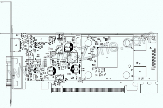
The GT218 will be the first 40nm based GPU rolling out from Nvidia and word has it there are at least 4 SKUs on different PCB designs (something that has yet to be 100% confirmed). The following image was scooped up by outside sources and gives us a glimpse of what the hardware might actually look like. It is based on the P692 PCB design codenamed D10M1-30. Core clock rate is 550MHz and the shader clock comes in at 1375MHz while memory is expected to be introduced at 512MB DDR3 at 800MHz on a 64bit interface. The exact number of shader processors has not been revealed as of current however the card is expected to have typical support for Dual Link DVI, DisplayPort, VGA and all the other common things.
As we can see from the image above, this PCB design is low-profile and from what we gather in the technical drawing, a low-profile adapter will accommodate or at least be available so that the card could be installed into a low-profile Home Theater PC (HTPC) or other small form factor chassis including 2U height boxes with cards that install vertically. We can also see that connector “J2” on the backplane, above the DVI connector could be an S-Video output, which makes a common appearance on low profile cards.
This is the only technical drawing we were able to find, and it is based only on one PCB design, there are apparently more – hopefully they will surface sooner than CeBIT in March and we can give you more insight.
Get Tom's Hardware's best news and in-depth reviews, straight to your inbox.
-
timaahhh 512 MB at 64bits? Is there a point to that? Why would you not buy a lower end card from a previous generation?Reply -
Mr_Man I thought the GTX 2xx naming scheme was supposed to make things less confusing... where do they get the idea for GT218?Reply -
Tindytim Mr_ManI thought the GTX 2xx naming scheme was supposed to make things less confusing... where do they get the idea for GT218?Reply
The GTX 280, 260, 285, and 295 are all based on the GT200 core. This is a new core, the GT218. -
megamanx00 Guess this will have lower memory bandwidth than the 4550 so I suppose it may be a 4350 competitor. Either way it won't exactly be a gaming card ^_^.Reply -
eklipz330 this just in:Reply
nVidia's NOT renaming this time...
with all due respect, i understand taking the the older generation, renaming, and possibly lowering its hierarchy and price to fit the naming scheme making room for newer cards... but renaming, and increasing the price just isn't nice -
ubergeetar I dont get it... It's a new core, with ZERO improvements on memory, core speed, etc. Even if it has more processors, wouldnt the 64-bit interface would really slow things down? Why take such a huge step back from DDR3 512bit?Reply -
stridervm I think the idea is for nVidia to make careful, but baby steps regarding it's new video card.... Process.Reply
If you remember they only just recently relesed their 55nm video cards, and then jumping into another lower process, that takes guts as it's a real gamble. I think they're just playing safe. -
nottheking Uber, this is a lower-end card. While very wide memory interfaces are nice, there are some extra costs they bring that cannot simply be taken away through revisions to smaller fabrication processes.Reply
Basically, the wider the memory interface, the more pins your package needs, and the more interconnects inside the GPU package has to have, all of which require so much edge space. Basically, looking at what GPUs I've been able to gather data on, the lower-end of die size necessary for a given memory interface width is in the neighborhood of the following:
■128-bit: 100 mm²
■256-bit: 196 mm²
■512-bit: 420 mm²
Bigger die sizes equals a greater liklihood of having a chip be bad, and fewer chips cut from a wafer to begin with, resulting in greatly increased prices. This is why, in spite of the advantages in performance it'd bring, no one moves their entire lineup to use wider memory interfaces: it'd require bigger chips.
Furthermore, the wider the interface, the more RAM chips you need to actually use it. I believe a minimum of 1 DRAM chip per 32 bits of interface width is standard for video cards; hence, a 512-bit interface requires a whopping 16 DRAM chips; not good for prices.
Basically, I'm guessing this will probably pack around 8 ROPs, 16 or 32 TMUs, and 32 or 64 stream processors; it will be a low-end part, probably designed, yes, to compete with the Radeon 4550. Looking at it, I'd say that the reason behind these decisions is that their recent beatings have forced nVidia to a more conservative ground, where they're making their first test with a product that will cost them very, very little to make, and will have a volume market that their traditional flagships do not, and could hopefuly restore them to profitability. -
nottheking Bleh, I failed up there, assuming these comments followed the same code as the forums... And no "preview comment" option. Just ignore the ugly tags; it was supposed to be bullet-points, obviously.Reply

