GDDR7 Arrives: Samsung Outs World's First Chip, 32 GT/s for Next-Gen GPUs
Samsung's GDDR7 promises a 20% improvement of power efficiency over GDDR6 .

Get Tom's Hardware's best news and in-depth reviews, straight to your inbox.
You are now subscribed
Your newsletter sign-up was successful
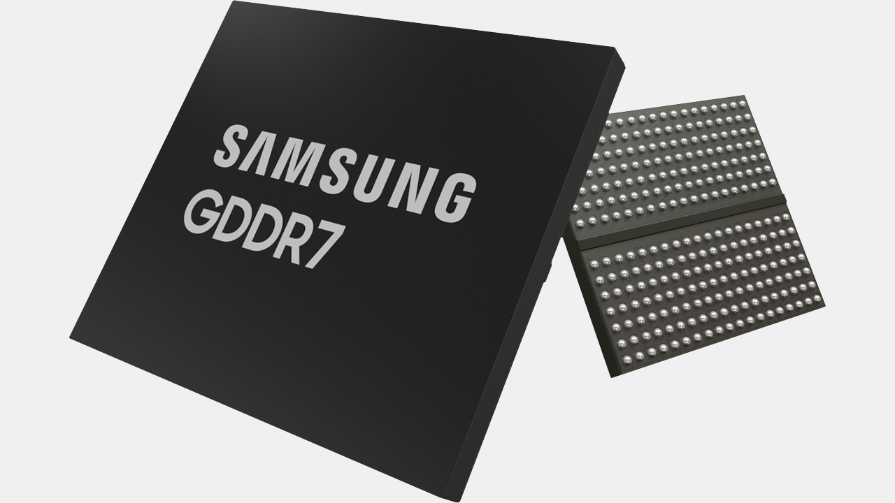
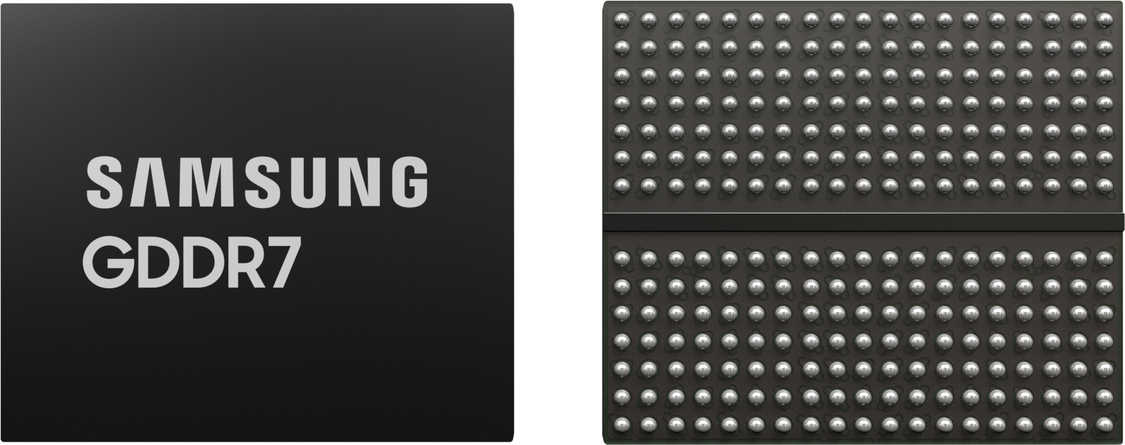
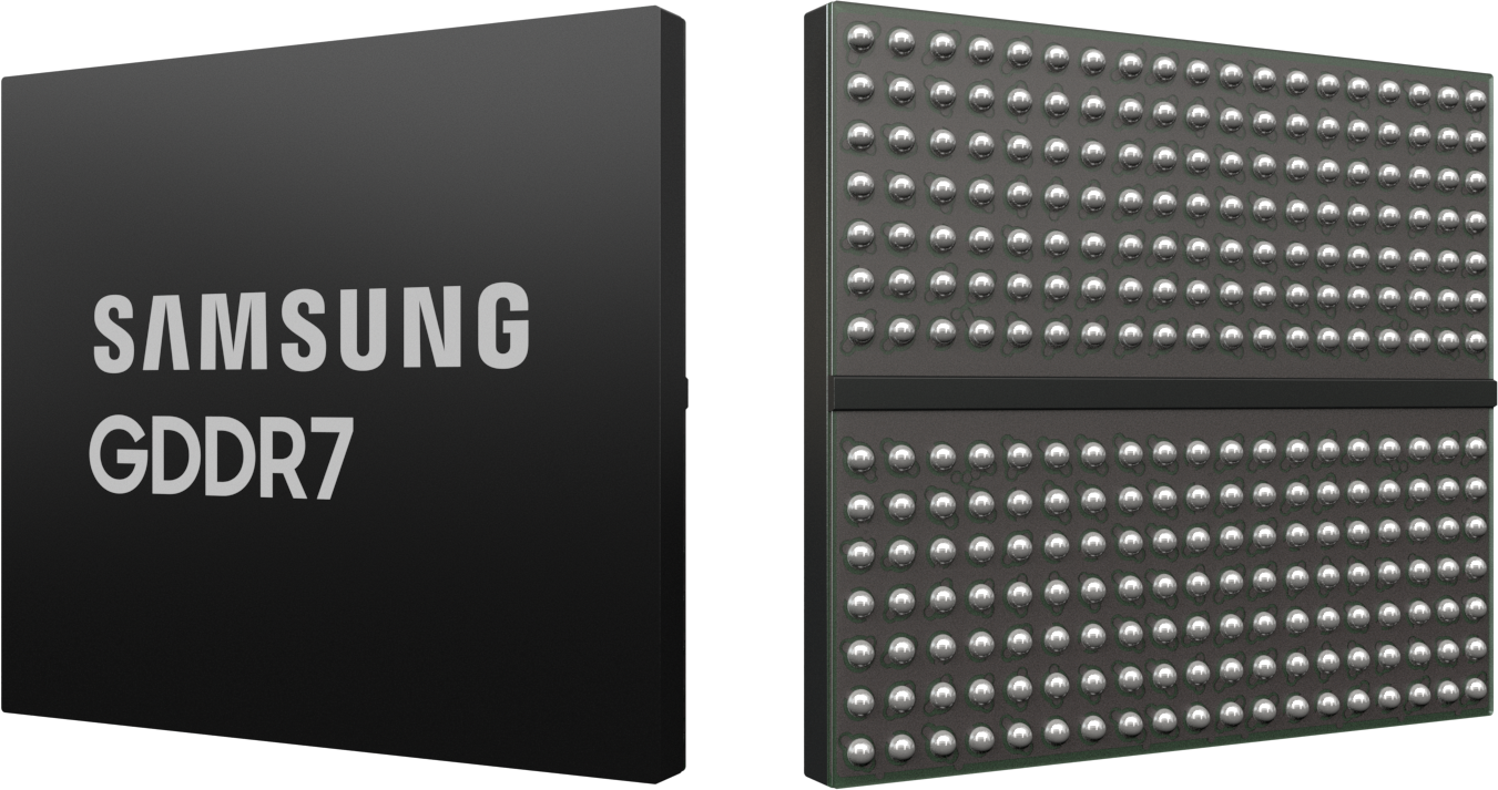
In a quite unexpected twist, Samsung late on Thursday said that it had completed the development of the industry's first GDDR7 memory chip. The new device will feature a data transfer rate of 32 GT/s, use pulse-amplitude modulation (PAM3) signaling, and promise a 20% power efficiency improvement over GDDR6. To achieve this, Samsung had to implement several new technologies.
Samsung's first 16Gb GDDR7 device features a data transfer rate of 32 GT/s and therefore boasts a bandwidth of 128 GB/s, up significantly from 89.6 GB/s per chip provided by GDDR6X at 22.4 GT/s. To put it into perspective, a 384-bit memory subsystem featuring 32 GT/s GDDR7 chips would provide a whopping 1.536 TB/s of bandwidth, which by far exceeds GeForce RTX 4090's 1.008 TB/s.
To hit unprecedentedly high data transfer rates, GDDR7 uses PAM3 signaling, a kind of pulse amplitude modulation featuring three distinct signaling levels (-1, 0, and +1). This mechanism enables the transfer of three bits of data within two cycles, which is more efficient than the two-level NRZ, which is the method used by GDDR6. However, it is important to note that PAM3 signals are more complex to generate and decode than NRZ signals (which means additional power consumption), and they can be more susceptible to noise and interference. Meanwhile, it looks like the benefits of PAM3 outweigh its challenges, so it is set to be adopted by both GDDR7 and USB4 v2.
In addition to higher performance, Samsung's 32 GT/s GDDR7 chip is also said to feature a 20% improvement in power efficiency compared to 24 GT/s GDDR6, though Samsung does not specify how it measures power efficiency. Typically, memory makers tend to measure power per transferred bit, which is a fair thing to do, and from this point of view, GDDR7 promises to be more efficient than GDDR6.
Meanwhile, this does not mean that GDDR7 memory chips and GDDR7 memory controllers will consume less than today's GDDR6 ICs and controllers. PAM3 encoding/decoding is more complex and will require more power. In fact, Samsung even goes on to say that it used an epoxy molding compound (EMC) with high thermal conductivity and a 70% lower thermal resistance for GDDR7 packaging to ensure that the active components (the IC itself) do not overheat, which is an indicator that GDDR7 memory devices are hotter than GDDR6 memory devices, especially when working at high clocks.
It is also noteworthy that Samsung's GDDR7 components will offer a low operating voltage option for applications like laptops, but the company does not disclose what kind of performance we should expect from such devices.
Truth be told, Samsung's announcement is a little bit shy of details. The company does not say when it plans to start mass production of its GDDR7 components and which process technology it is set to use. Given the cadence of new GPU architecture announcements by AMD and Nvidia — every two years — it is logical to expect next-generation graphics processors to hit the market in 2024, and they are more than likely to adopt GDDR7.
Get Tom's Hardware's best news and in-depth reviews, straight to your inbox.
Meanwhile, Samsung expects artificial intelligence, high-performance computing, and automotive applications to take advantage of GDDR7 as well, so perhaps some sort of AI or HPC ASICs may adopt GDDR7 ahead of GPUs.
"Our GDDR7 DRAM will help elevate user experiences in areas that require outstanding graphic performance, such as workstations, PCs and game consoles, and is expected to expand into future applications such as AI, high-performance computing (HPC) and automotive vehicles," said Yongcheol Bae, Executive Vice President of Memory Product Planning Team at Samsung Electronics. "The next-generation graphics DRAM will be brought to market in line with industry demand and we plan on continuing our leadership in the space."

Anton Shilov is a contributing writer at Tom’s Hardware. Over the past couple of decades, he has covered everything from CPUs and GPUs to supercomputers and from modern process technologies and latest fab tools to high-tech industry trends.
-
emike09 And Nvidia will still skimp on VRAM and charge insane prices for higher-memory models. Looking at you, 16GB 4060 Ti.Reply -
thestryker This announcement would have been significantly more meaningful if they were talking 32Gb capacities given the current trend of sliced bus width.Reply -
bit_user IIRC, doesn't GDDR6X use PAM4 signalling?Reply
Also, I seem to recall something about GDDR7 using on-die ECC, like DDR5. That could help explain additional power consumption by the DRAM chips. -
thestryker Reply
Yeah Micron debuted PAM4 with GDDR6X.bit_user said:IIRC, doesn't GDDR6X use PAM4 signalling?
Everything starting with GDDR5 has had memory error correction, but there may be more specifics for GDDR7 as I haven't read up on it yet.bit_user said:Also, I seem to recall something about GDDR7 using on-die ECC, like DDR5. That could help explain additional power consumption by the DRAM chips. -
bit_user Reply
Source? I can't find any indication of that, on any GDDR standards, actually.thestryker said:Everything starting with GDDR5 has had memory error correction, but there may be more specifics for GDDR7 as I haven't read up on it yet.
And are we talking just at the interface level, on-die, or both? -
thestryker Reply
For VRAM I believe it's always been controller level except for ECC of course. I think the GDDR part is CRC (Micron docs refer to data link protection), but it has to be read by the controller it doesn't do it by itself.bit_user said:Source? I can't find any indication of that, on any GDDR standards, actually.
And are we talking just at the interface level, on-die, or both? -
InvalidError Reply
Based on all of the criticism and 16GB failing to smooth out some dips as expected due to the 128bits bottleneck, we can only hope Nvidia learned the lesson that 128bits simply wasn't enough for the 4060(Ti) and it won't do that again. Releasing generation upon generation of GPUs that get thrashed by reviews and rot on shelves is not good for business.emike09 said:And Nvidia will still skimp on VRAM and charge insane prices for higher-memory models. Looking at you, 16GB 4060 Ti. -
hotaru.hino Reply
Considering Samsung only announced a 16Gb (2GB) chip, they're going to have to charge more for VRAM anyway because that would require extra memory interfaces, which need L2 cache. Unless NVIDIA copies AMD, VRAM capacity and bus-width are going to be issues here.emike09 said:And Nvidia will still skimp on VRAM and charge insane prices for higher-memory models. Looking at you, 16GB 4060 Ti.
Really I find it more disappointing a 32Gb (4GB) chip wasn't announced. -
InvalidError Reply
24Gbits chips are already getting somewhat on the large side at ~120sqmm. You are going to have to wait until either the next cell shrink, stacked DRAM packages (ex.: basically do HBM but switch out the HBM base die with a (G)DDRx one) or multi-layer DRAM chips for 32Gbits.hotaru.hino said:Really I find it more disappointing a 32Gb (4GB) chip wasn't announced. -
thestryker Reply
It's not a packaging problem as Samsung already has GDDR6W which runs 32Gb because it combines two 16Gb in one package. That doesn't mean there isn't a feasibility of manufacture issue at hand for a single 32Gb chip of course.InvalidError said:24Gbits chips are already getting somewhat on the large side at ~120sqmm. You are going to have to wait until either the next cell shrink, stacked DRAM packages (ex.: basically do HBM but switch out the HBM base die with a (G)DDRx one) or multi-layer DRAM chips for 32Gbits.

