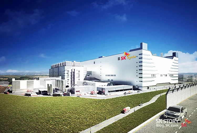
SK hynix late on Wednesday announced that it had decided to build its new advanced memory packaging facility in Indiana, which will start operations in the second half of 2028. Given the timeline, the facility will almost certainly work on HBM4 and HBM4E memory products. In addition, SK hynix inked an R&D deal with Purdue University.
The advanced memory packaging facility will require roughly $3.87 billion in investments from SK hynix and is said to come online sometime in the back half of 2028. The plant will not process wafers with memory circuits, but will get them from elsewhere (presumably from SK hynix's South Korean fabs), and then assemble HBM from known good stacked dies (KGSDs) consisting of multiple memory dies on top of a base die.
HBM memory is used on some of the most advanced processors for AI and HPC, including AMD's Instinct MI300-series and Nvidia's H100/H200 and B100/B200-series products. Having an HBM packaging facility in the U.S. will make the supply chain of high-bandwidth memory somewhat more resilient, but SK hynix will keep making HBM memory devices in South Korea, based on the company's current announcements.
"We are excited to become the first in the industry to build a state-of-the-art advanced packaging facility for AI products in the United States that will help strengthen supply-chain resilience and develop a local semiconductor ecosystem," said SK hynix CEO Kwak Noh-Jung. "With this new facility, we hope to advance our goal of providing AI memory chips with unmatched capabilities, serving the needs of our customers."
The plant will be located in West Lafayette, Indiana, which seems a somewhat strange place to build an advanced memory packaging facility. SK hynix says that the location was chosen because of Indiana's robust industrial infrastructure: an R&D ecosystem led by Purdue University and Ivy Tech Community College; the presence of experts in the semiconductor field; availability of skilled talent from Purdue University; and significant support offered by state and local governments.
Also, SK hynix intends to collaborate with Purdue University for future research and development (R&D) projects. Furthermore, West Lafayette, Indiana, is located about 250 miles west of Columbus, Ohio, where Intel is building its Silicon Heartland production site that will consist of multiple fab phases and will require investments of over $100 billion to be fully built. Also, Intel has an advanced chip packaging facility in Arizona, whereas TSMC is expected to construct its own advanced logic packaging facility in the same state, eventually.
To ensure that it will have enough qualified engineers at its advanced memory packaging facility, SK hynix intends to work in partnership with Purdue University and Ivy Tech Community College to create training programs and multidisciplinary degree courses aimed at nurturing a skilled workforce in high-tech fields and establishing a consistent stream of emerging talent.
"SK hynix is the global pioneer and dominant market leader in memory chips for AI," Purdue University President Mung Chiang said. "This transformational investment reflects our state and university's tremendous strength in semiconductors, hardware AI, and hard tech corridor. It is also a monumental moment for completing the supply chain of digital economy in our country through chips advanced packaging. Located at Purdue Research Park, the largest facility of its kind at a U.S. university will grow and succeed through innovation."
