Samsung Densifies M.2 SSDs With PoP Controller, Forges Ahead With New Spec
Samsung's Global SSD Summit in Korea is always the location of the company's biggest announcements, and this year's event was no exception. Samsung unveiled its new 960 Pro and Evo models, which brought the anticipated increases in performance and capacity, but the company also outlined a new advance in SSD controller technology that promises to bring about a sea change in M.2 SSD designs. Samsung is also forging ahead with a new density-increasing form factor that it outlined (briefly) at the Flash Memory Summit.
Densifying M.2 With PoP
One of Samsung's most interesting revelations is the addition of a package on package (PoP) design for its Polaris SSD controllers. PoP designs, which combine the memory and the logic into one discrete package with two components, have been a staple in the mobile segment for over a decade. In some respects, it is surprising that it took this long for PoP to make it into SSD designs, but economics may have been the true hurdle.
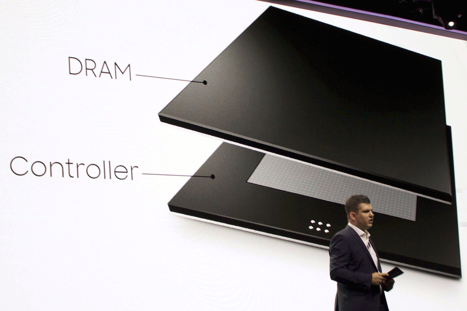
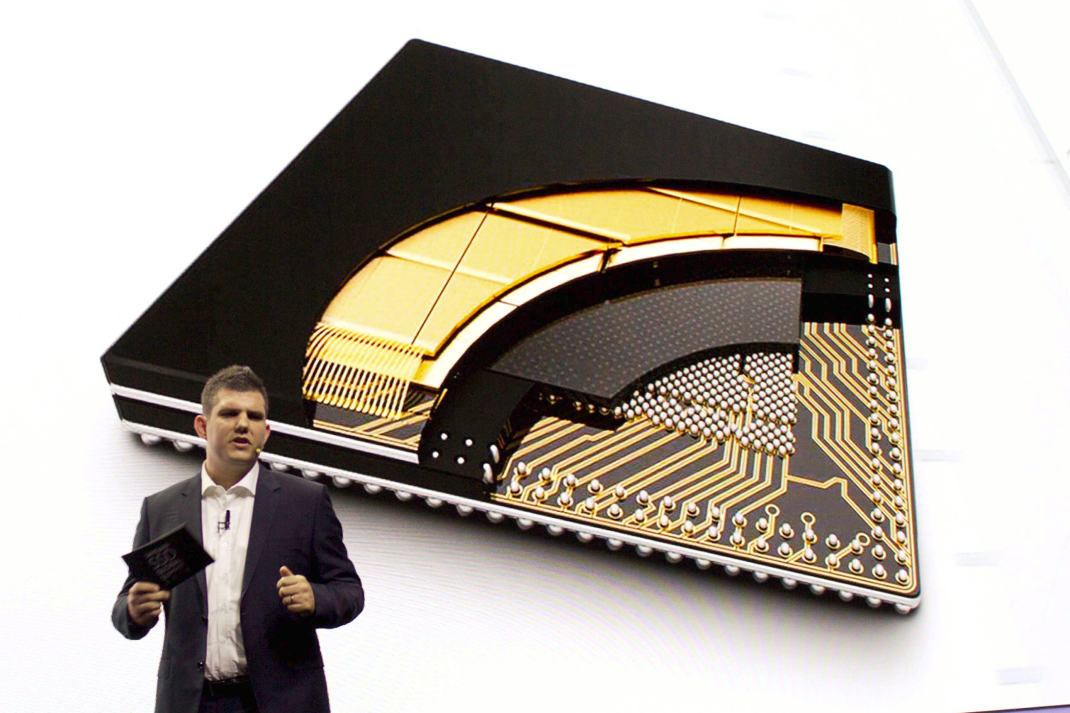
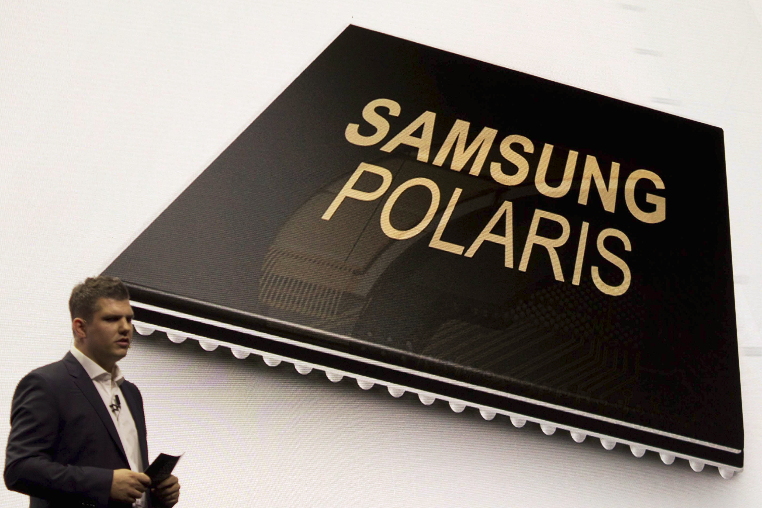
The technique is fairly straightforward: The SSD controller (logic) resides on an underlying substrate that has an array of BGA (Ball Grid Connectors) underneath, just as with a normal BGA-mounted controller. The PoP aspect comes into play when the vendor places a DRAM package on the top of the controller. The DRAM package connects through two additional rows of BGA connectors that ring the underlying controller. As with any standard design, the logic resides on the bottom of the stack due to its need for more connectors.
Article continues belowThere are several advantages to PoP designs, with density being the primary consideration for M.2 SSDs. High-performance SSDs require a DRAM cache to hold the LBA tables, which speeds the process of locating data held on the NAND. The DRAM package consumes space on the PCB, which reduces the number of NAND packages that the vendor can pack into the small form factor.
Most M.2 SSDs have only NAND components on one side of the PCB, which is referred to as a single-sided design. Vendors can mount additional packages on the bottom of the PCB (double-sided) to increase density. Unfortunately, most notebooks and mobile devices support only single-sided M.2 SSDs because the slimmer SSDs offer a lower profile for thin designs. The need to pack as much NAND as possible on one side of the SSD turns every square millimeter of the PCB into precious real estate.
Removing the separate DRAM component from the SSD allows Samsung to include additional NAND packages on the PCB, which increases storage capacity and performance. As a result, Samsung can cram in four 16-die packages onto the 960 Pro, which brings capacity up to 2TB. Using a PoP controller likely increases production costs to some extent, but Samsung has extensive experience with the technology through its line of mobile SoCs. Scale is always helpful to defray production costs, and Samsung has it in spades.
Samsung's vertical integration provides it with a key advantage over its competitors that extends beyond cost. For instance, NAND is the most expensive component on an SSD. In contrast to popular belief, the SSD controller is really only a very small part of the BOM (Build Of Materials) cost, with prices projected between $5 to $15 apiece. However, having access to one's own controller technology provides a faster time to market and tighter integration.
Get Tom's Hardware's best news and in-depth reviews, straight to your inbox.
In many cases, utilizing a third-party SSD controller is like trying to fit a square peg into a round hole. Third-party SSD controller vendors, which almost all of the major fabs use, design their controllers to work with several types of NAND from multiple vendors. Accommodating for a wide range of 2D and 3D NAND in SLC, MLC, TLC (and now QLC) flavors means that there is less targeted optimization for the vendors' specific NAND. In many cases, SSD vendors that utilize third-party controllers also have to interact with the SSD controller vendor to get important fixes and optimizations pushed through the pipeline, which increases the time to market and reduces flexibility. Also, the NAND fabs don't want to give away all of their secrets, so information sharing becomes a major concern. Adding in contractual constraints only complicates the process. Samsung and Toshiba both have their own organic SSD controller programs, which cuts through all of the red tape.
Samsung's new PoP design is yet another advantage, but the third-party SSD controller vendors will likely follow suit. PoP designs require the ultimate in integration and experience, so it will be interesting to see how the industry reacts. There is a pronounced industry-wide move to the M.2 form factor, so PoP could be a big advantage in the hottest market segment. Samsung has dominated the SSD market for several years by leading the race to 3D NAND. The other fabs are finally shipping 3D NAND, which levels the playing field, but PoP may just be the next Samsung advantage for the next few years.
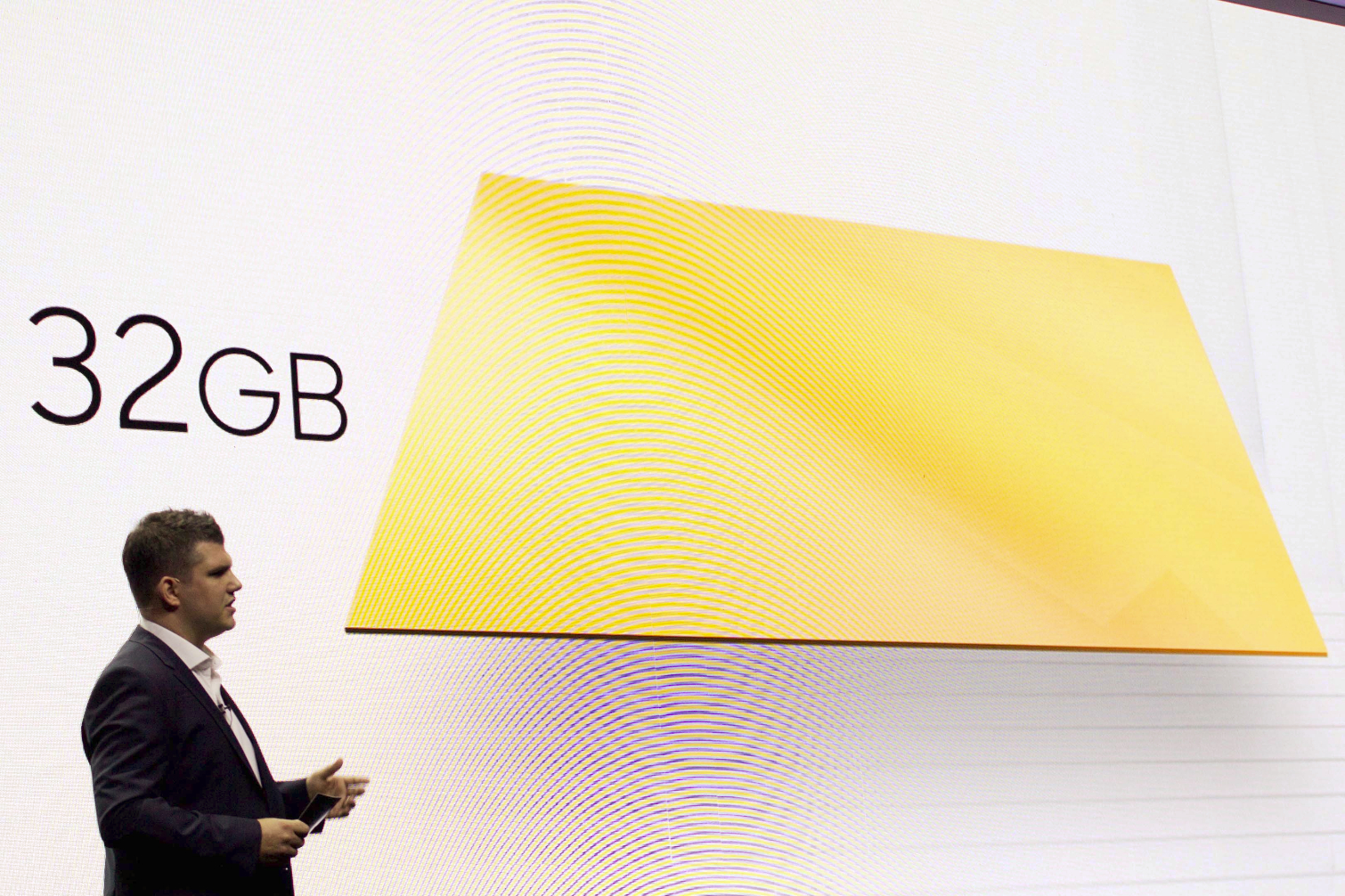
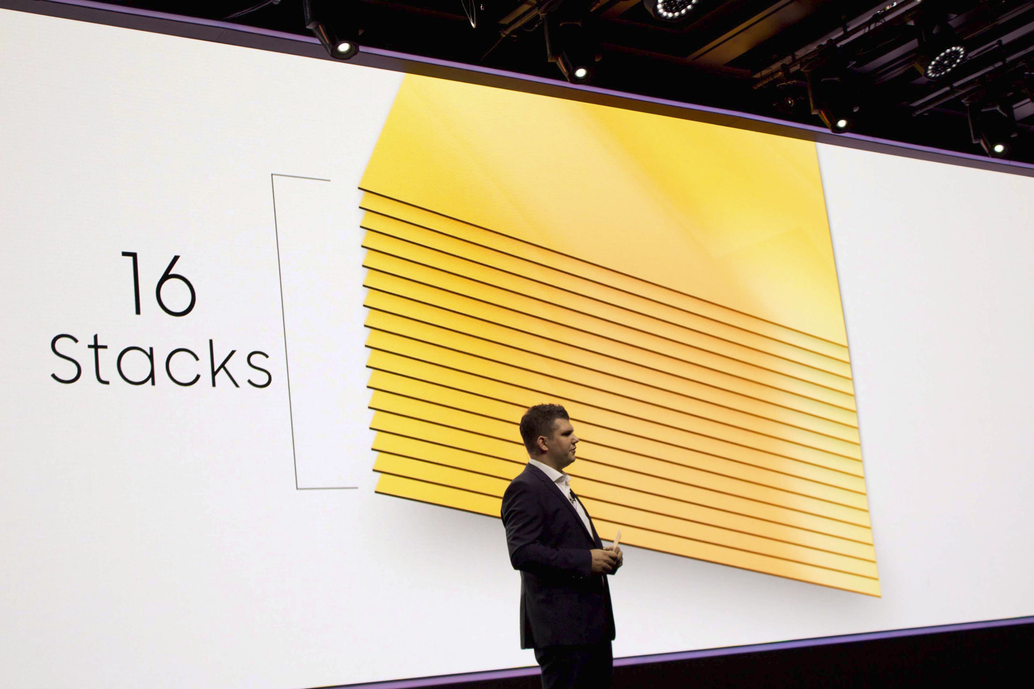
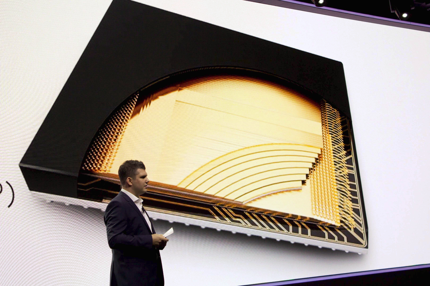
Samsung also touted its 16-die stack technology as another key to its new 2TB SSDs--but it isn't new. Each die has 48-layers, but NAND fabricators stack the die atop each other to increase density. SSD manufacturers tend to shy away from using 16-die stacks because of manufacturing complexity. Samsung's move to the dense packages likely indicates that it has surmounted the manufacturing challenges associated with wire bonding the die together. Higher die stacks also lead to reduced performance due to increased impedance from longer wires. We know that Samsung is already using small F-chips in some 48-layer NAND die, which helps to defray the performance loss associated with the increased impedance, so it already solved the performance challenges.
A New Form Factor Beckons
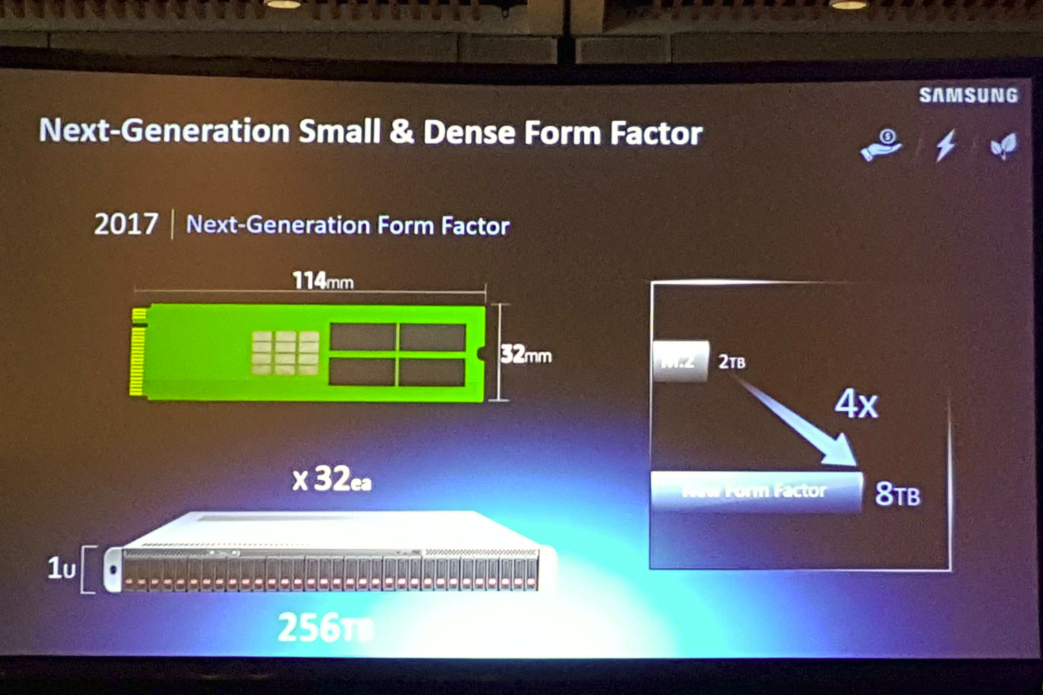
Samsung is also working on a new form factor SSD that will increase density in enterprise environments. Intel famously led the M.2 form factor charge, which it named the "Next Generation Form Factor" (NGFF) before the standards committees shortened the name to the friendlier "M.2." Samsung is driving the next initiative, which it also describes as an NGFF form factor, albeit with the addition of the "Small & Dense" tagline.
The new form factor measures 32 x 114mm, which is much wider than current designs. The increased width allows Samsung to place two rows of NAND chips on each side of the PCB. The technique will increase density up to 8TB per SSD, which easily outweighs any existing products.
Another important addition is a modified latching mechanism. You have to slide current M.2 SSDs into the connector at an angle, and then you latch the SSD downward to lock it into position. The latching mechanism makes it nearly impossible to use M.2 SSDs in the front bay of a server, which hampers adoption. Enterprise users require hot-swappability (another feature M.2 lacks) and front-accessibility to ease servicing. The new Samsung form factor will support both features, and the server rendering indicates that the new SSDs will likely fit into somewhat normal drive sleds.
Samsung is working with the standards committees, much like Intel did with the first NGFF form factor, to foster widespread adoption. A standardized approach means we may eventually see the new form factor from other manufacturers.
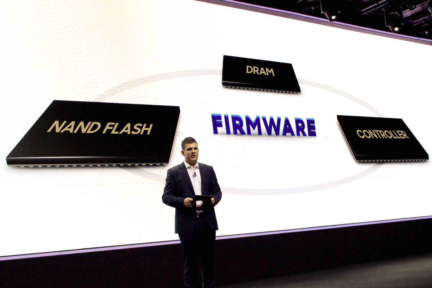
Density is one of the key advantages of SSDs; we always want faster devices with more capacity in smaller packages. Samsung has all four of the most important aspects of an SSD (NAND, controller, DRAM, and firmware) directly under its own control. The company is working on several fronts to increase its capabilities, and in many respects, dragging the rest of the industry along with it.

Paul Alcorn is the Editor-in-Chief for Tom's Hardware US. He also writes news and reviews on CPUs, storage, and enterprise hardware.
-
pocketdrummer Too bad they don't curate the ads they put on their website. Whenever they use services like that, it just results in clutter and scams.Reply -
Game256 Is there any info about more concrete 960 release date (like beginning of October or late October)? NewEgg is already accepting pre-orders.Reply -
CRamseyer We honestly have no idea when they will ship. I heard the samples came back to the US the same day we returned but we do not have samples, a spec sheet or release date information yet.Reply -
Patrick_Bateman I don't get why SSDs are so expensive? They are physically smaller and have no moving parts, which hard drives do. Is it because NAND purity has to be very high? Or is it because the vendors just set a price that most consumers would be ok with? Still waiting for a 100$ 1 TB 3D NAND SSD.Reply -
CRamseyer The fabs to make the flash cost 5 billion Dollars and take several years to build. The technology changes roughly every 18 months and each change requires new tools, new processes and so on. Imagine what a car would cost if each year and a half a new design had to come out.Reply -
Bruce427 Chris,Reply
Would your expectation be that the new Samsung 400GB EVO 960 will be superior to the 256GB Pro 950 in pretty much every performance parameter?
I had planned on replacing several 256GB Pro 950s with Pro 960s, but Samsung didn't choose to offer a 256GB pro version. -
rpg1966 "SSD manufacturers tend to shy away from using 16-die stacks because of manufacturing complexity" ...and "We know that Samsung is already using small F-chips in some 48-layer NAND packages".Reply
Here, is the number of dies in the "stacks", the same as the number of "layers"?
So whilst 16-die stacks are avoided by some, Samsung (and others) are doing 48- or 64-layers? -
Paul Alcorn Reply18653602 said:"SSD manufacturers tend to shy away from using 16-die stacks because of manufacturing complexity" ...and "We know that Samsung is already using small F-chips in some 48-layer NAND packages".
Here, is the number of dies in the "stacks", the same as the number of "layers"?
So whilst 16-die stacks are avoided by some, Samsung (and others) are doing 48- or 64-layers?
Each die has 48 layers of cells.
The individual die are stacked, 16 of them.
So, in effect, that would be 768 layers of data cells.

