SK Hynix Introduces '4D NAND'
SK Hynix unveiled its future roadmap of new flash products here at the Flash Memory Summit. But in a case of the marketing department straying too far from reality, the company has branded the new flash as "4D NAND." That implies a new dimension added to the garden-variety 3D flash, but it looks eerily similar to a technology pioneered by Intel and Micron, albeit with a few other existing flash technologies sprinkled in.

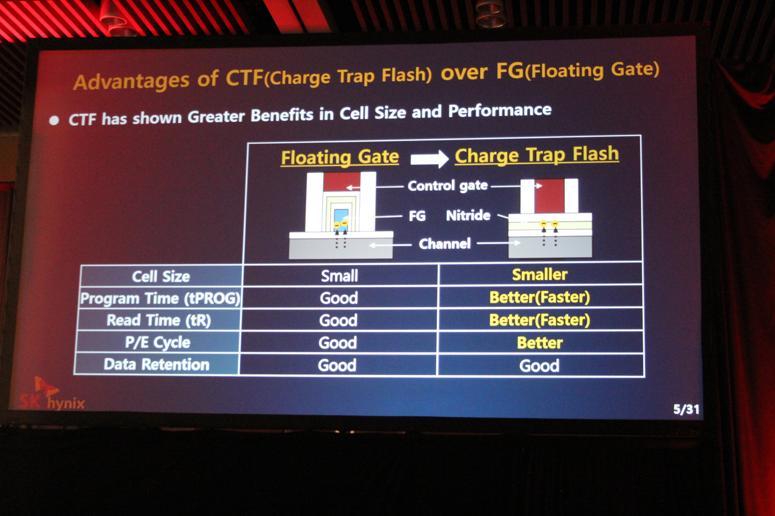
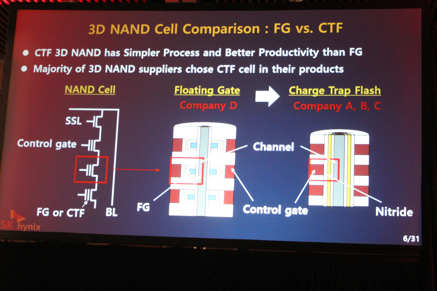
SK Hynix's new 4D NAND uses a charge trap design, just like the flash produced by Samsung and WD/Toshiba. SK Hynix has used Charge Trap Flash (CTF) designs for several years, so it isn't new, and currently Micron and Intel are the only two flash-fabbers using floating gate technology. Intel and Micron plan to diverge on their flash development efforts after their next-gen flash comes to market, after which Micron will use its own 'Replacement Gate' technology, which is simply a re-branded Charge Trap Flash design. In other words, Intel will soon be the only flash producer using floating gate technology.
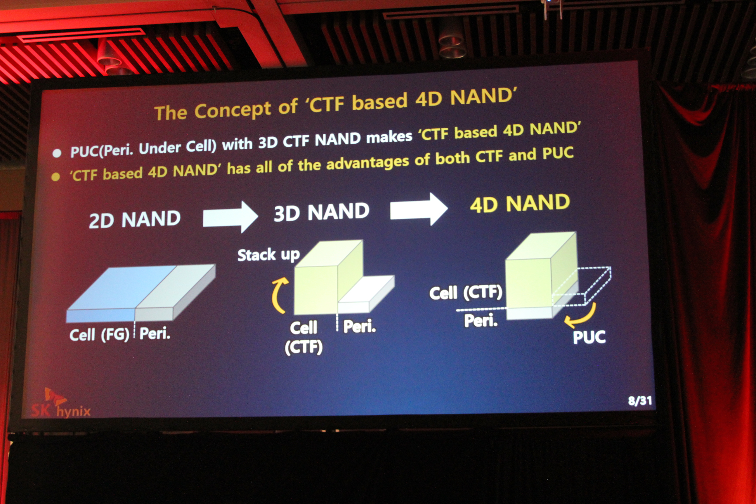
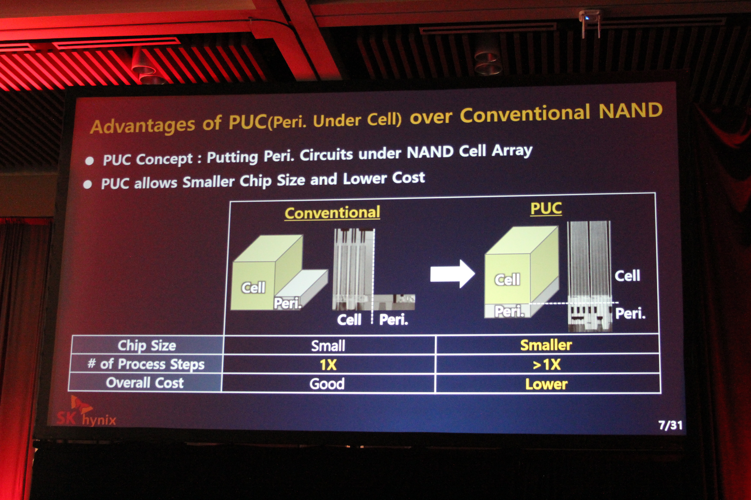
So what separates SK Hynix's 4D NAND from the 3D NAND competitors? The company touts its CTF design paired with its Periphery Under Cell (PUC) technology. In short, 3D flash consists of two primary components: the array and the periphery circuitry. Just like every other 3D NAND, SK Hynix's array is a vertical stack of layers that stores data, and the periphery circuitry lines the edges of the die. This circuitry controls the array, but it consumes die space and increases in complexity and size as more NAND layers are added. That added complexity and size increases the cost of the end product.
Article continues belowTo circumvent this issue, SK Hynix's 4D NAND uses the PUC design, which places the circuitry under the array instead of around it. This tactic increases density, and thus reduces cost. However, this is the same design that Intel and Micron pioneered with their very first generation of 3D flash, though they refer to it as "CMOS under Array" (CuA). Samsung has also announced that it's moving to a CuA-type design in the future, so this tactic is definitely not new.
As such, SK Hynix's rebranding of existing technologies certainly does not take NAND into the fourth dimension. While we've yet to see how this new NAND will perform, 4D NAND as a technology brand seems to mostly be marketing gone wild.
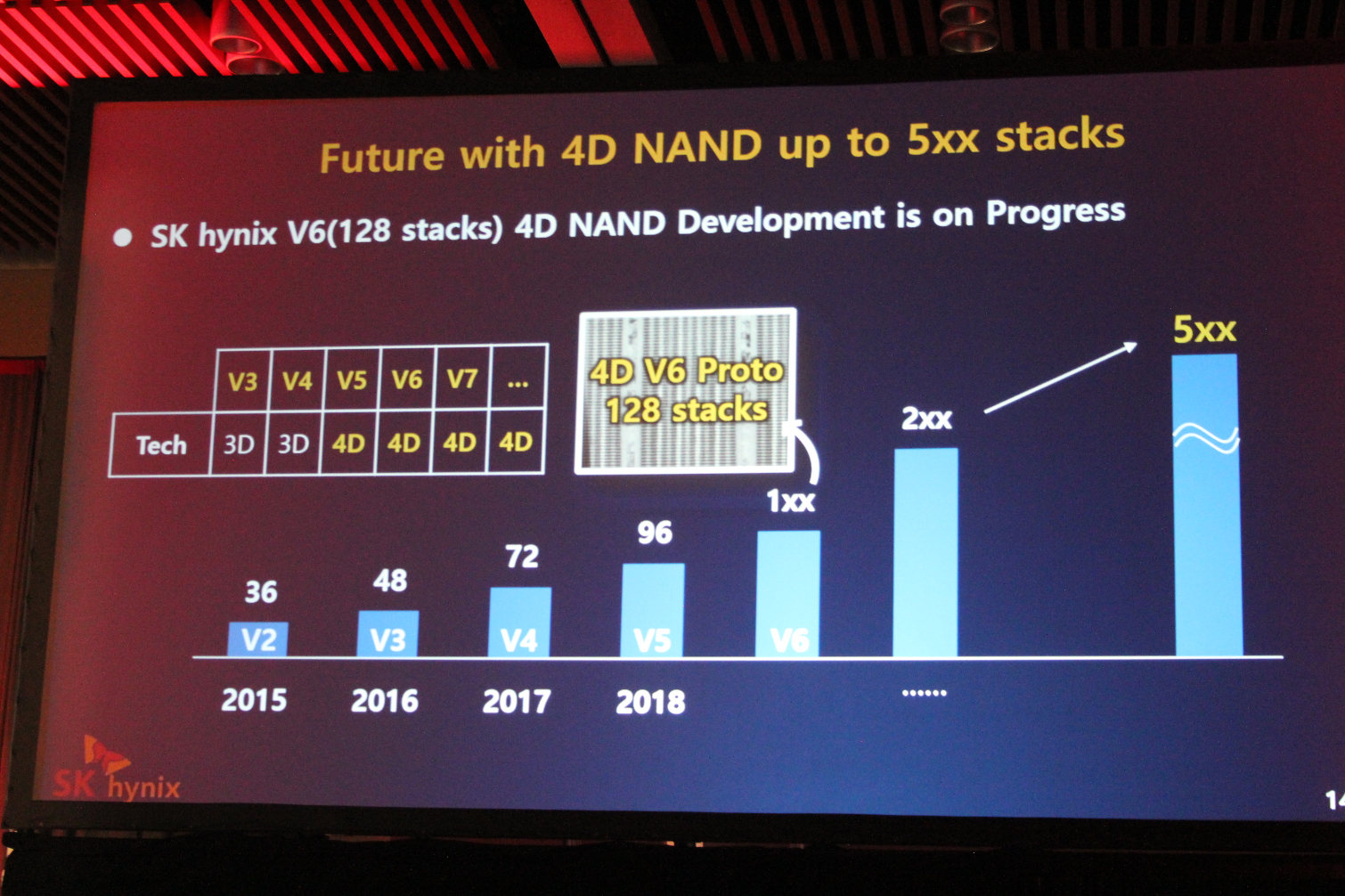
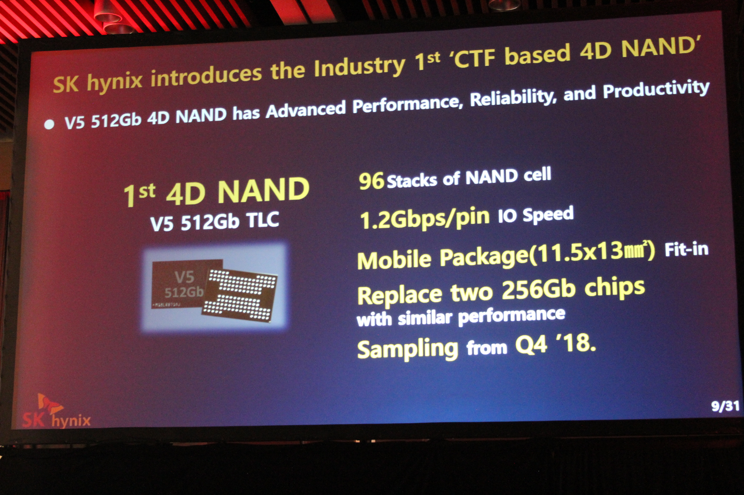
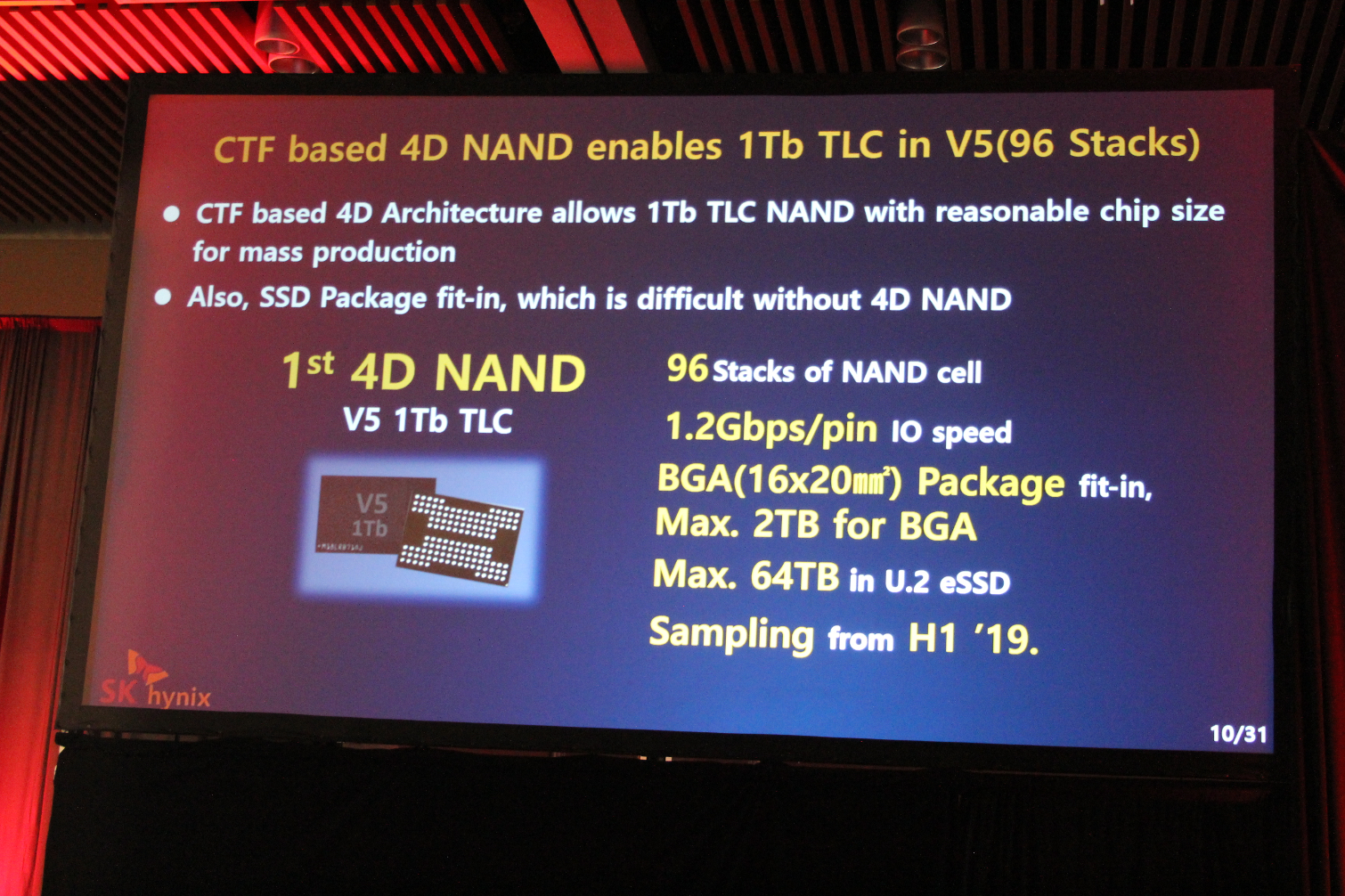
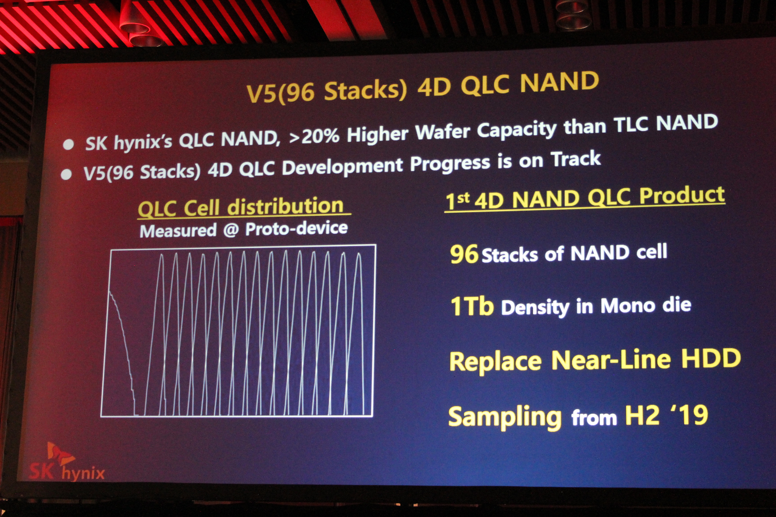
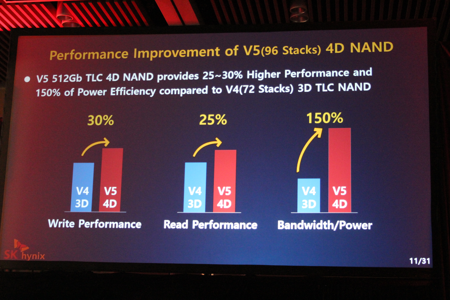
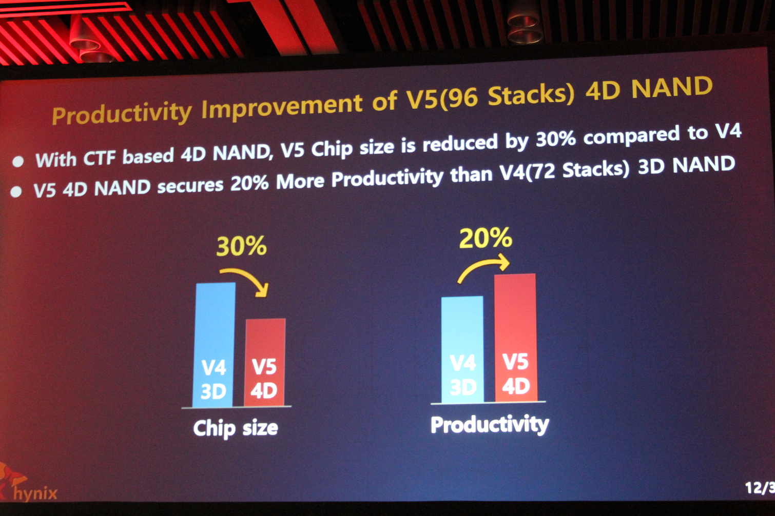
All that aside, SK Hynix does have an impressive-looking roadmap. The company will sample its first-gen 4D NAND in Q4 2018. The 96-layer TLC flash will come as standard 1Tb die for SSDs and a 512Gb die for BGA packages. The company also has QLC 4D NAND in development. This variant of the 96-layer flash will come to market in the second half of 2019, which is well behind the other flash-fabbers that are either shipping QLC products or have them coming to market this year.
SK Hynix sees a path forward to 500-layer 4D NAND, but hasn't specified a timeline for the product.
Get Tom's Hardware's best news and in-depth reviews, straight to your inbox.

Paul Alcorn is the Editor-in-Chief for Tom's Hardware US. He also writes news and reviews on CPUs, storage, and enterprise hardware.
-
derekullo Reply21214479 said:The 4th dimension NAND... cmon... who is the genius who named it 4D...
I bet that person was a "Doctor"
-
littleleo Samsung has their 3-bit MLC marketing hype, lol! Just makes you wonder how stupid do they think we are? Oh wait Trump is pres they are right.Reply -
jpe1701 Why can't I just scroll down and see the stories in order like I used to? Now I have to click back and choose the stories. Does it make more clicks for ad revenue or something?Reply -
Darkbreeze "There is a fourth dimension, beyond that which is known to man. It is a dimension as vast as space, and as timeless as infinity. It is the middle ground between light and shadow, between science and superstition, and it lies between the pit of man's fears and the summit of his knowledge. This is the dimension of imagination. It is an area which we call The Nand Zone."Reply -
enewmen Reply21214583 said:21214479 said:The 4th dimension NAND... cmon... who is the genius who named it 4D...
I bet that person was a "Doctor"
Yup ! -
cookiemania66 Reply21216459 said:"There is a fourth dimension, beyond that which is known to man. It is a dimension as vast as space, and as timeless as infinity. It is the middle ground between light and shadow, between science and superstition, and it lies between the pit of man's fears and the summit of his knowledge. This is the dimension of imagination. It is an area which we call The Nand Zone."
You sir. you would be a better president then this orange with his corn hair -
littleleo Reply
So would my Cat and he doesn't send tweets he eats them.21216512 said:21216459 said:"There is a fourth dimension, beyond that which is known to man. It is a dimension as vast as space, and as timeless as infinity. It is the middle ground between light and shadow, between science and superstition, and it lies between the pit of man's fears and the summit of his knowledge. This is the dimension of imagination. It is an area which we call The Nand Zone."
You sir. you would be a better president then this orange with his corn hair
-
USAFRet Reply21216459 said:"There is a fourth dimension, beyond that which is known to man. It is a dimension as vast as space, and as timeless as infinity. It is the middle ground between light and shadow, between science and superstition, and it lies between the pit of man's fears and the summit of his knowledge. This is the dimension of imagination. It is an area which we call The Nand Zone."
I wonder when we will find the outer edge of this type of technology. There may be a limit somewhere.