Engineer creates CPU from scratch in two weeks — begins work on GPUs
The finished design is heading for TinyTapeout 6
Get Tom's Hardware's best news and in-depth reviews, straight to your inbox.
You are now subscribed
Your newsletter sign-up was successful
An engineer has shared his experience of designing a CPU from scratch, over two weeks, “with no prior experience.” During this brief period, Adam Majmudar claims to have learned the fundamentals of chip architecture, absorbed the finer points of chip fabrication, and prepared his first full chip layout using EDA tools. The next step in his “speed-running the chip stack” to-do list is designing a GPU from scratch. When finished this project is destined for production via Matthew Venn’s TinyTapeout 6.
We’ve reported on enthusiast DIY CPU designs previously, as well as DIY GPU projects. However, some of those feats have eaten through years of spare time for the people involved. Majmudar must be on vacation and spending all his surplus time on this “speed run” project to have gotten as far as he has “from scratch.”
I've spent the past ~2 weeks trying to make a chip from scratch with no prior experience. It's been an incredible source of learning so far.Progress tracker in thread (coolest stuff at the end)👇 pic.twitter.com/tKuYg7GgdIApril 11, 2024
The fledgling chip designer, who describes himself as one of the founding engineers at a web3 development company, outlines the steps he has made so far in his quest. You can click and read through all the steps leading up to the current GPU focus via the embedded Tweet, above. We’ve also bullet-pointed the speed run steps which have been completed to date, below.
Article continues below- Learning the fundamentals of chip architecture – a strong understanding is a critical foundation
- Learning the fundamentals of chip fabrication – materials, wafer prep, patterning and packaging
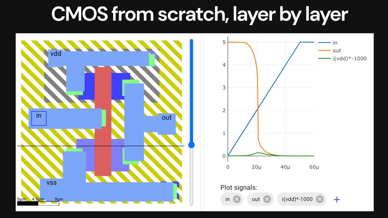
- Starting electronic design automation by making a CMOS transistor, layer-by-layer
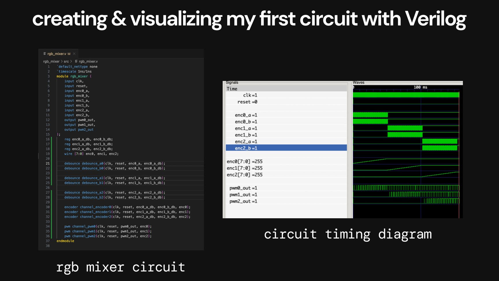
- Creating my first full circuit in Verilog – “my first experience with programming hardware using software.”
- Implementing simulation & formal verification for my circuit
- Designing my first full chip layout – designing and optimizing using OpenLane, which is an open-source EDA tool
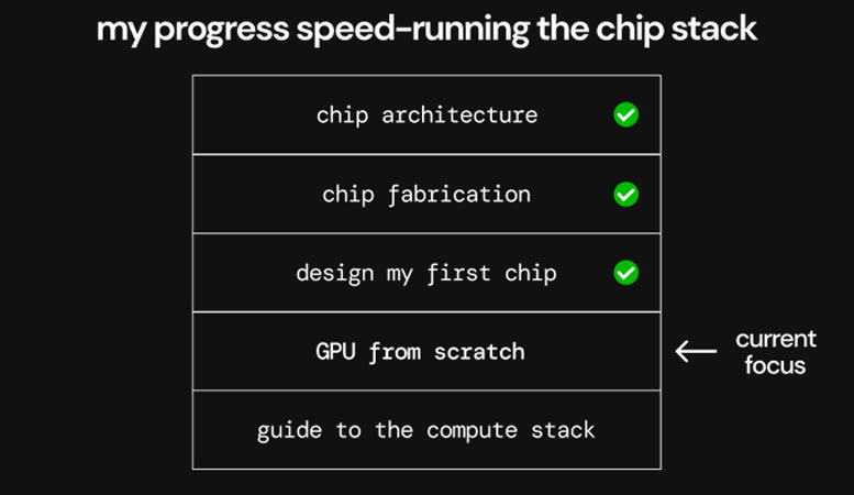
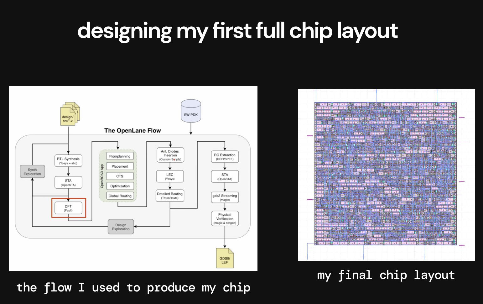

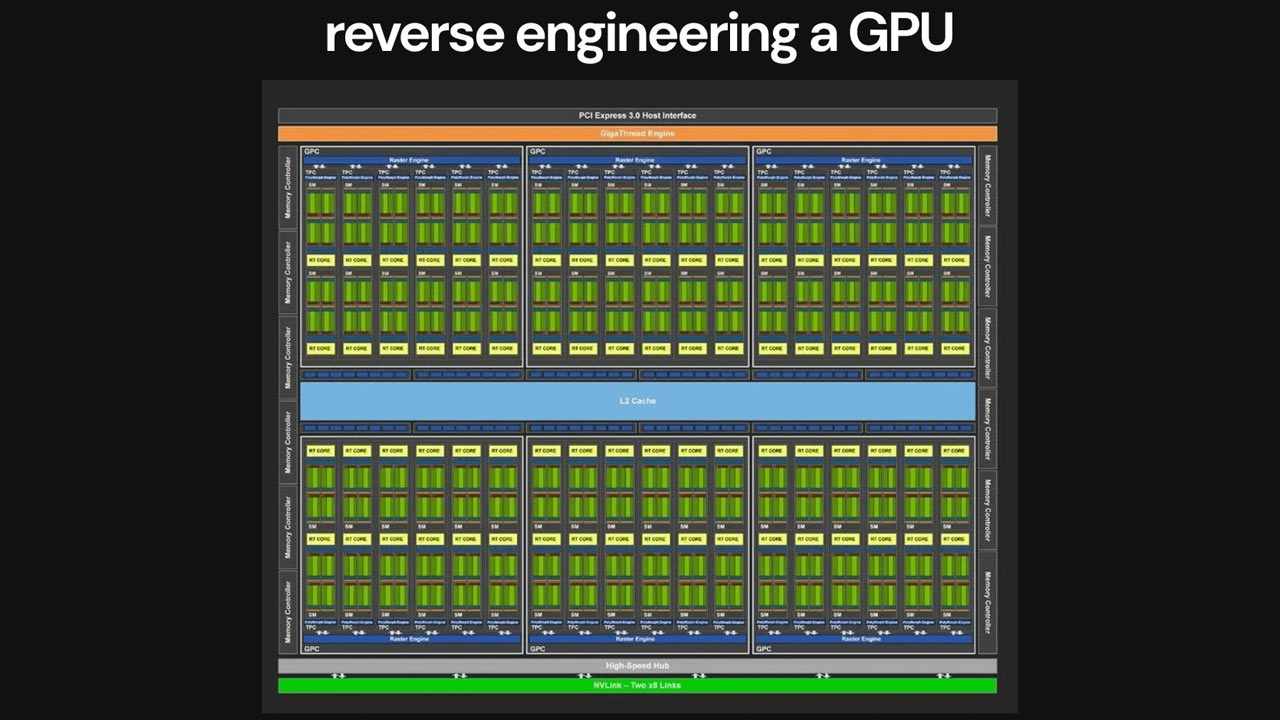
As we mentioned in the intro, the significant step that Majmudar now faces is designing a GPU from scratch. He knows this will be a difficult task and admits that, after initial investigations, it is harder than expected. The fledgling chip designer explains that there simply aren’t the learning resources online for building a GPU. “Because GPU companies are all trying to keep their secrets from each other, most of the GPU architecture data is all proprietary and closed source,” the engineer finds.
Despite this hurdle, Majmudar says the big GPU-makers’ secrecy has made this part of the project “way more fun for me.” Interestingly, Anthropic’s Claude Opus AI tools have been useful during this GPU designing stage. “I've been proposing my ideas for how each unit must work to Claude, and then somehow it will guide me toward the right implementation approaches which I can then go and confirm with open-source repos,” explained the engineer. However, he observed that “if I search some of the things publicly, nothing shows up which is a testament to how well hidden the implementation details are.”
After taking just two weeks or so to get through three out of five legs of his speed run, the above concerns expressed regarding GPUs might make readers worry that Majmudar may have hit a speed bump, a snag, or even a brick wall. That doesn’t seem to be the case, as he optimistically predicts that his GPU design will be shipping “in the next few days,” and a cut-down version sent to be taped out.
It may be well worth keeping an eye open for this engineer’s next updates. However, we know it can take quite some time between submitting work to projects like TinyTapeout and the production run. The maker of the Rickroll ASIC, for example, said there were nine months between submitting his design and receiving the silicon. Please note that TT06 closes just eight days from now.
Get Tom's Hardware's best news and in-depth reviews, straight to your inbox.

Mark Tyson is a news editor at Tom's Hardware. He enjoys covering the full breadth of PC tech; from business and semiconductor design to products approaching the edge of reason.
-
Blastomonas I don't believe that this is true. I suspect that some exaggeration is going on here..Reply -
why_wolf I'm imagining this is creating a "functional" but not "useful" CPU. So something that can maybe run "Hello, World" and that's it.Reply -
Blastomonas Reply
This would make more sense.why_wolf said:I'm imagining this is creating a "functional" but not "useful" CPU. So something that can maybe run "Hello, World" and that's it.
I struggle to accept that an engineer had no relatable experience in chip design before deciding to make one. The idea that one Monday morning this guy decided to build a cpu from scratch with no knowledge and then 14 days later its ready to go seems unlikely to me.
Genius level inteligence or down playing their own knowledge and experience? I believe that people go to university for years to learn the skills and knowledge to do this. -
Conor Stewart Learning things quickly isn't always a good thing.Reply
Creating my first full circuit in Verilog – “my first experience with programming hardware using software.”
This is an example, by using verilog you are not programming hardware using software, verilog is not a software programming language, it is a hardware description language. Yes you could argue they mean using software to synthesize and implement the hardware but I doubt this is what they mean. Too many people, especially software engineers which they claim to be, treat verilog and VHDL as just another programming language.
Something definitely seems off too, it would be hard but possible to go from no knowledge to a basic CPU in two weeks, however it would not be any more than a demonstration, there is pretty much no way they went from no knowledge to an actually useful CPU in just two weeks unless they copied others work. Based on the fact they mention using some kind of AI and open source projects for learning this might be the case.
It could also just be that this is an awful design but it does technically work, maybe something like Ben Eater's breadboard computer that I believe only had 16 bytes of memory and was 8 bit. It does work well enough to run a simple program like incrementing a counter or performing basic calculations but it is not useful in any way other than just for learning.
If I remember bitluni's video on his tiny tapeout design then the cells they were allowed were very small and he pretty much implemented a ROM and he couldn't manage to fit much in, so it ended up being a very small ROM and even then used up 4 of the available cells (I think bitluni was given a chance just because they had space to fill so that may be why he was allowed 4 cells, also he wasn't given much notice or time to finish it which also probably also means it was just to fill space). So making a CPU within tiny tapeout, it either has to have no on board memory or it is a very very basic CPU with very little memory.
I think there is probably a reason that people haven't implemented usable CPUs (like RISC-V) on tiny tapeout before.
Edit: looking at tiny tapeout 6, someone may be trying to make a RISC-V EC processor on it but I'm not sure how functional it will be. -
rfdevil ReplyConor Stewart said:Learning things quickly isn't always a good thing.
This is an example, by using verilog you are not programming hardware using software, verilog is not a software programming language, it is a hardware description language. Yes you could argue they mean using software to synthesize and implement the hardware but I doubt this is what they mean. Too many people, especially software engineers which they claim to be, treat verilog and VHDL as just another programming language.
Something definitely seems off too, it would be hard but possible to go from no knowledge to a basic CPU in two weeks, however it would not be any more than a demonstration, there is pretty much no way they went from no knowledge to an actually useful CPU in just two weeks unless they copied others work. Based on the fact they mention using some kind of AI and open source projects for learning this might be the case.
It could also just be that this is an awful design but it does technically work, maybe something like Ben Eater's breadboard computer that I believe only had 16 bytes of memory and was 8 bit. It does work well enough to run a simple program like incrementing a counter or performing basic calculations but it is not useful in any way other than just for learning.
If I remember bitluni's video on his tiny tapeout design then the cells they were allowed were very small and he pretty much implemented a ROM and he couldn't manage to fit much in, so it ended up being a very small ROM and even then used up 4 of the available cells (I think bitluni was given a chance just because they had space to fill so that may be why he was allowed 4 cells, also he wasn't given much notice or time to finish it which also probably also means it was just to fill space). So making a CPU within tiny tapeout, it either has to have no on board memory or it is a very very basic CPU with very little memory.
I think there is probably a reason that people haven't implemented usable CPUs (like RISC-V) on tiny tapeout before.
Edit: looking at tiny tapeout 6, someone may be trying to make a RISC-V EC processor on it but I'm not sure how functional it will be.
If you check the twitter thread, he didn't create a CPU, or anything close to one. As far as I can tell, he just took some circuits that others created (e.g., debouncer, pwm) and hooked them up to create a 3 channel LED controller that can output a pulse signal. That's it. He did go through the rest of the flow (synthesis, STA, P&R, etc.) but it seems to be the core only, there's no pads or anything to connect the chip to a package, it's just the core logic.
He has not sent the design for fabrication (it would be rejected anyway) and doesn't seem to have a plan to do so. His plan is to now jump to reverse engineering a full GPU and tape that out. I give him an A+ for effort and self motivation, but he is not anywhere near as far along the path of designing any kind of real processor that he seems to think he is. -
CmdrShepard Reply
This article sports a clickbait headline which is as misleading as the one about the developer "hacking" Denuvo DRM.artk2219 said:I wonder what the specs are and if he's actually gotten any code to run on it.
The headline says "Engineer creates CPU from scratch in two weeks" and burries the lede again by leaving the most important detail for the end.
CPU has not been created -- it has only been designed.
We don't even know if his design was validated and whether he wants to tape it out, let alone what kind of CPU he was designing (i.e. 32-bit or 64-bit? RISC or something else? How many registers? Size of instruction set?).
We don't have ballpark figures on the node size it will be made in, how many CPUs will be made, how much it's going to cost, as well as what are expected power consumption, working frequency, and performance.
We don't know whether he already has a dev toolchain for it nor whether he even intends to follow up and write some code for it.
We don't get any information about the Tiny Tapeout 6 but are left to research that on our own.
Oh, and we don't get any information about what university this guy has finished if any. People studying computer science on university of electrical engineering in my country get to design their own RISC CPU as part of their study so this is maybe nothing more than putting that kind of knowledge to use.
TL;DR -- Instead of providing us with useful info like what I just enumerated above, this vapid, pointless, article does literally no effort to answer any of the questions its lack of facts raises. -
CmdrShepard Reply
Thank you for doing the research the author of this miserable clickbait fluff article didn't bother to do before submitting it. If I could have upvoted you more than once I would have.rfdevil said:If you check the twitter thread, he didn't create a CPU, or anything close to one. As far as I can tell, he just took some circuits that others created (e.g., debouncer, pwm) and hooked them up to create a 3 channel LED controller that can output a pulse signal. That's it. He did go through the rest of the flow (synthesis, STA, P&R, etc.) but it seems to be the core only, there's no pads or anything to connect the chip to a package, it's just the core logic.
He has not sent the design for fabrication (it would be rejected anyway) and doesn't seem to have a plan to do so. His plan is to now jump to reverse engineering a full GPU and tape that out. I give him an A+ for effort and self motivation, but he is not anywhere near as far along the path of designing any kind of real processor that he seems to think he is. -
DevL0rd I've done this in 3 days before.Reply
https://circuitverse.org/users/17603/projects/16-bit-computer-be083c00-104f-4bec-bfea-0cdc0126e9bc
Only experience was MC redstone lol
There is more of us nerds out there than you think ❤️