U.S. Semiconductor Renaissance: All the Upcoming Fabs
Everything we know about new chip manufacturing facilities in America.
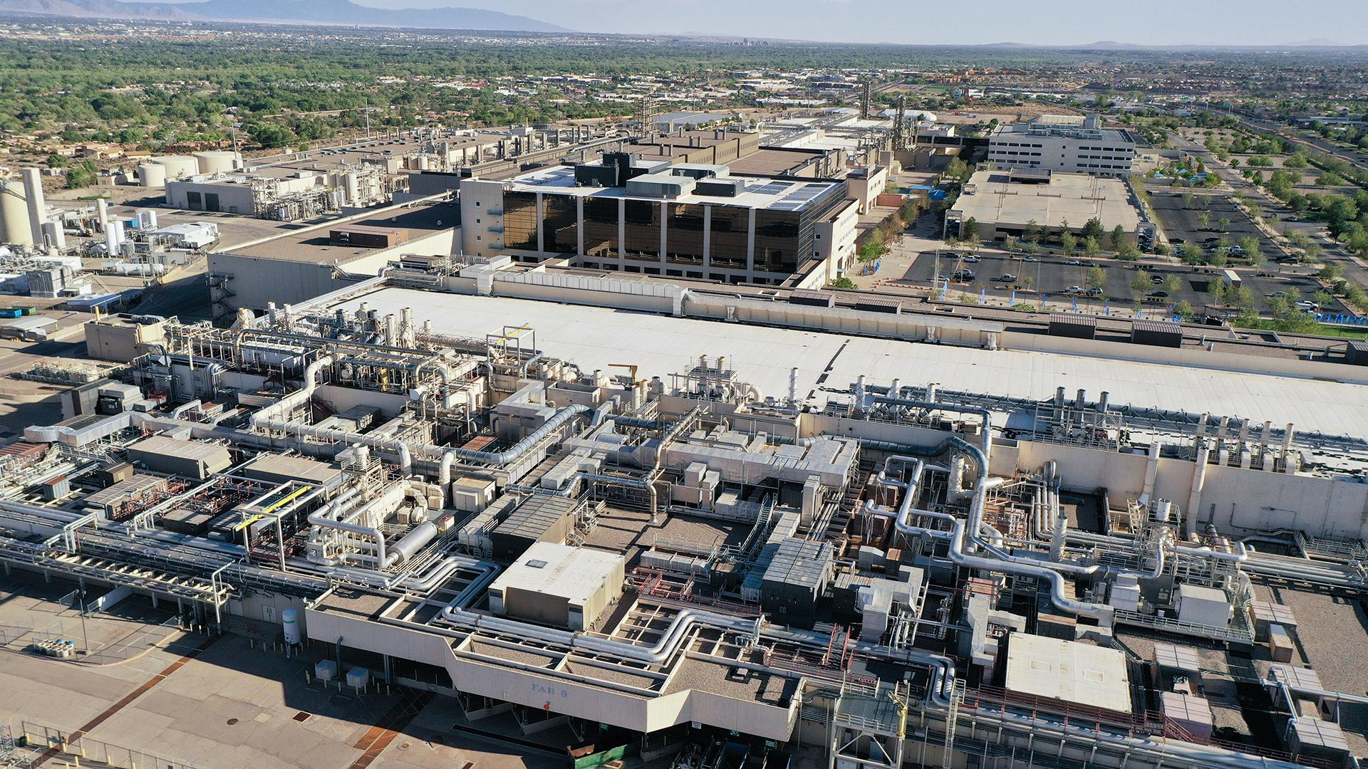
The U.S. share of global semiconductor manufacturing capacity has decreased from 37% in 1990 to 12% in 2021, according to the Semiconductor Industry Association (SIA), but some 47% of the chips sold worldwide are designed in the U.S. This disparity poses major risks to American national security and the economy, which is why both industry insiders and politicians recently began to call for building semiconductor fabs in the USA.
Their calls have been heard, and today five major chipmakers — GlobalFoundries, Intel, Samsung Foundry, TSMC, and Texas Instruments — are building new semiconductor production facilities in the U.S. These efforts will inevitably be bolstered by a new wave of funding provided by the newly-approved CHIPS act. This U.S. subsidy initiative will pump $52 billion into new US-based chip fabs and provide fresh tax incentives. Those funds will spur a wave of new investment over the coming years, and its sorely needed.
There are many reasons why countries like Taiwan, South Korea, and Singapore became leading producers of logic and memory chips in the 1990s and 2000s. In addition to lower labor costs in these states, those governments and their local authorities provided various incentives to chipmakers, which is why it was significantly cheaper to build fabs in Asia than in the U.S. and Europe.
New York and Saratoga County authorities understood this early and offered AMD significant incentives in 2006 when the company made plans for what is now known as GlobalFoundries Fab 8. Unfortunately, other states and the federal government weren't that agile, which is why the deployment of brand-new fabs became a rare occurrence in America. In fact, Intel even adjusted its manufacturing capacity strategy, culminating in it delaying the Fab 42 equipment move in by five years and its coming online by six years.
While we can't say that the semiconductor production industry in the U.S. didn't add capacity in recent years — both Intel and GlobalFoundries gradually expanded their production capacities in the late 2010s — brand-new leading-edge fabs haven't been deployed in the U.S. for a while. That's about to change. Here's how and where those changes will take place.
Intel: Spending Over $40 Billion on Chip Facilities in the U.S.
Intel is certainly one of the oldest chipmakers in the U.S. and one of the world's biggest. It also happens to be the only company spending more than $40 billion on new semiconductor fabs in the U.S. Unlike some of its industry peers that set long-term plans and option new fabs, Intel is investing tens of billions of dollars into four U.S. fabs that will come online in three years. Currently, Intel is building four chip production plants, two in Arizona and two in Ohio, and one advanced packaging facility in New Mexico.
Arizona
Get Tom's Hardware's best news and in-depth reviews, straight to your inbox.
Intel broke ground on Fab 52 and Fab 62 in the Ocotillo campus near Chandler, Arizona, in late September 2021, and the construction of those buildings is well underway. The fabs are designed to produce chips using Intel's 20A fabrication technology both for Intel and its Intel Foundry Services customers.
Intel's 20A production node will be the company's first process to incorporate RibbonFET gate-all-around field-effect transistors (GAAFETs) and PowerVia backside power delivery. These radical improvements are expected to bring significant power, performance, and area (PPA) improvements.
Intel's Fab 52 and Fab 62 will come online in 2024 and cost around $20 billion. These fabs will be instrumental for Intel's IDM 2.0 strategy that will find the company manufacturing chips for other companies, a first.
Ohio
Intel is building two fabs in Ohio that are yet to be named, but their significance for Intel and the U.S. chip industry is hard to overestimate. For years, Intel has gradually expanded its mega sites in Arizona, New Mexico, and Oregon. Expanding existing campuses makes a lot of sense since the semiconductor supply chain is very complex. Intel needs support from partners (e.g., raw materials suppliers, parts, etc.) with a local presence.
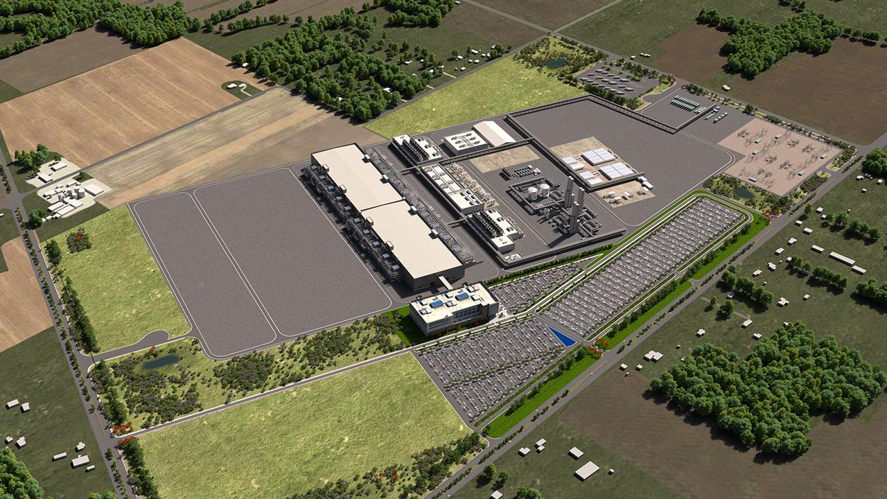
In Ohio, Intel wants to establish yet another mega site that will house up to eight semiconductor manufacturing facilities (we would include an advanced packaging facility, too, but Intel has not confirmed this). The site will require investments of around $100 billion to be fully built over the next decade. Furthermore, the new campus will require Intel's partners to establish a local presence, which essentially means a major expansion of the U.S. semiconductor supply chain. Actually, of all the chipmakers building new plants in the U.S., only Intel is willing to build a new mega-site from scratch.
The first two new fabs are near Columbus, Ohio, and are expected to produce chips on Intel's 18A/20A nodes sometime in 2025 when they come online. Intel's 18A manufacturing technology was meant to be the first fabrication process to take advantage of ASML's Twinscan EXE 0.55 High-NA extreme ultraviolet (EUV) lithography scanners. However, earlier this year, Intel said it could keep using current-gen Twinscan NXE 0.33 NA EUV tools for 18A by adopting multi-patterning. But even without High-NA tools, the new technology promises to bring a variety of power, performance, and area (PPA) advantages as it will rely on Intel's 2nd-Gen GAA RibbonFETs.
Intel's mega fab project will initially cost over $20 billion and will be Ohio's biggest economic development project in history. To lure Intel to Ohio, the state had to provide Intel with about $2.1 billion in various incentives. In addition, Intel is requesting funding from the federal government as part of the CHIPS act, but it isn't clear how much funding it will receive.
In fact, government funding is crucial for Intel's Ohio mega site project. Fab buildings are not expensive (but have the longest lead time), but semiconductor production tools are (e.g., one EUV scanner costs about $160 million). Intel can build shells, but then it needs to equip them with tools in a timely manner to meet its production schedules. Equipping a fab for a leading-edge node means buying all kinds of lithography (including immersion and EUV scanners), coating, etching, deposition, resist removal, inspection, and other tools, which cost billions of dollars.
If it takes too long to equip a brand-new chip plant due to a lack of financial resources, Intel can add extra tools to an existing facility to produce chips on a certain new node. But this means that Intel will have to put its new building on hold and wait for another opportunity to equip it, which means that it will generate costs without producing any earnings.
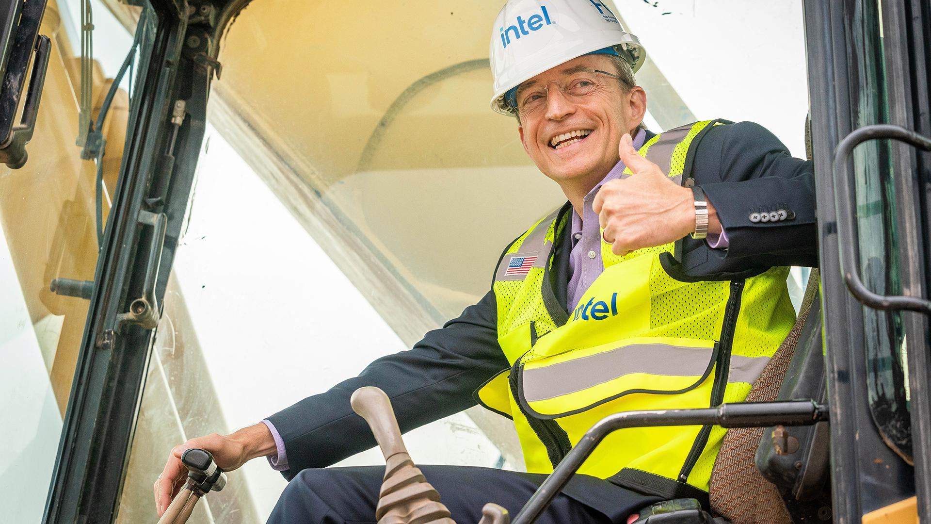
While Intel officially considers spare fab shells as a 'smart capital strategy' that gives it flexibility in how and when it brings additional capacity and tools online, it is still better to equip the buildings after they are constructed. This is why Intel CEO Pat Gelsinger warned the U.S. authorities and legislators that if the CHIPS act bill was not passed and the company didn't get financial incentives and support from the government, he might move the company's next mega site project to Europe.
New Mexico
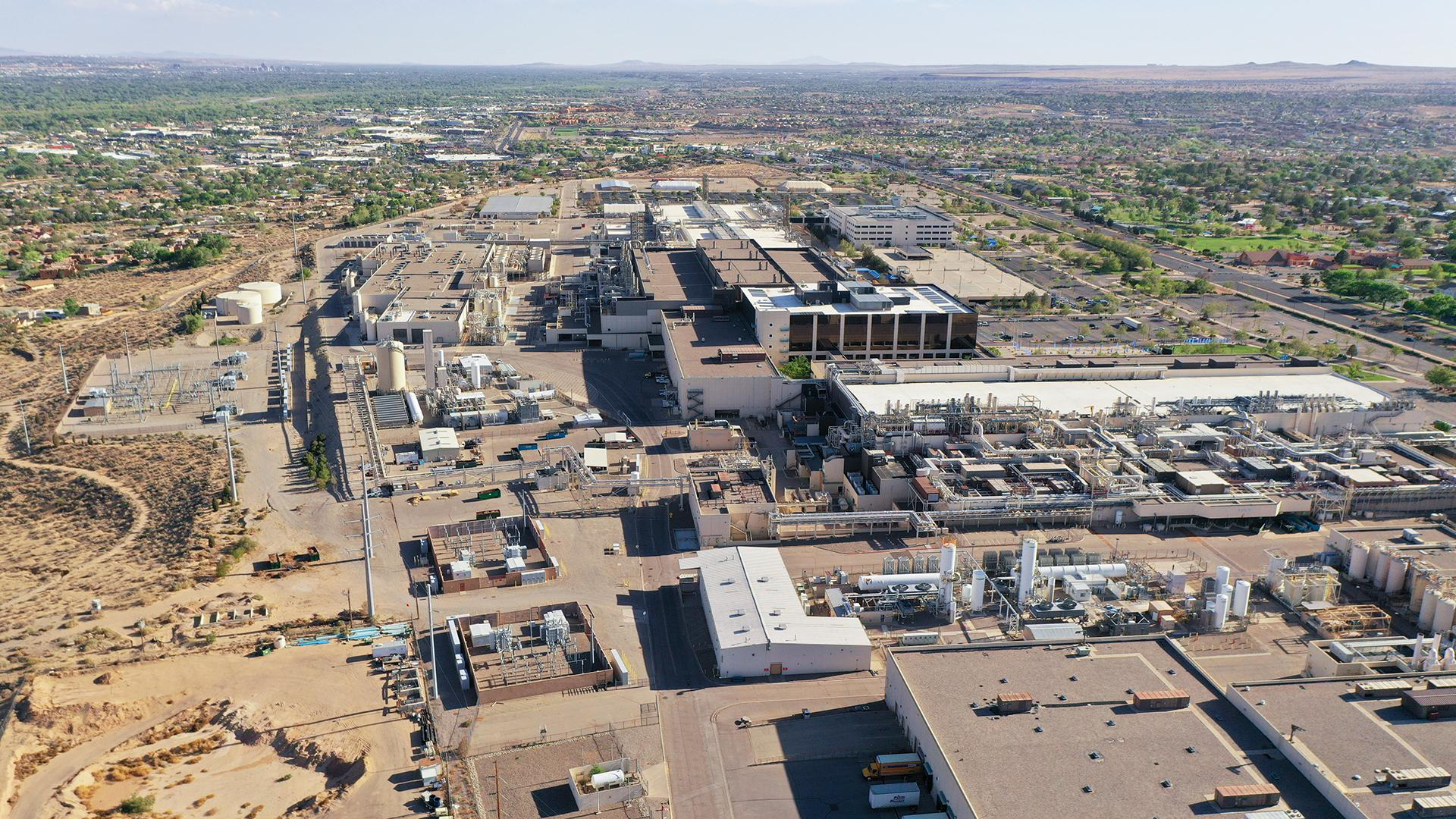
Intel's advanced packaging facility in New Mexico will enable the company and its clients to build complicated multi-chiplet designs (a-la Meteor Lake) that will become widespread in the coming years in the U.S.
Since sophisticated packaging technologies like embedded multi-die interconnect bridge (EMIB) and Foveros require a cleanroom, it is safe to call the packaging operations in New Mexico a fab. In fact, the equipment for the packaging facility will cost Intel $3.5 billion, the price of a new fab a couple of decades ago.
The advanced packaging operations will be instrumental for producing sophisticated designs in the U.S. when it becomes operational in 2023 ~ 2024, so this is yet another Intel project whose importance for the U.S. semiconductor industry is hard to overrate.
TSMC: 5nm Coming to the U.S.
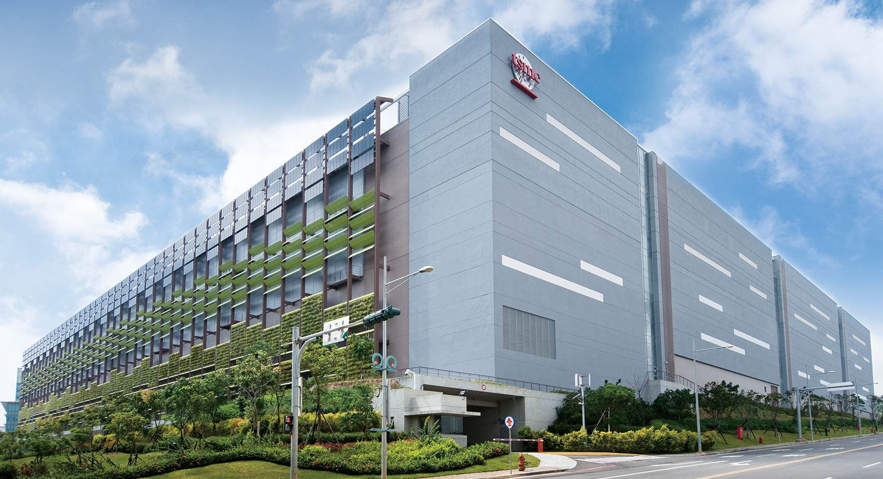
TSMC made quite a splash when it announced plans to build its 5nm-capable fab near Phoenix, Arizona, in mid-2020. Throughout its history, the company has only built two fabs outside of Taiwan — the WaferTech plant in Camas, Washington (which still processes 200-mm wafers using mature nodes) and Fab 16 in Nanjing, Jiangsu Province, China (which makes chips using TSMC's 28nm nodes). Therefore, the intention to build a fairly advanced fab in Arizona was considered a major shift in strategy.
Being the world's largest contract chipmaker, TSMC certainly has hundreds of customers in the USA, so bringing a fab closer to them might be beneficial. Yet, the first phase of the fab will have a capacity of around 20,000 WSPM (wafer starts per month) when it becomes operational in early 2024, which is significantly lower than the fabs that TSMC operates in Taiwan. Consequently, many observers view the project as a method to address some very specific customers serving the U.S. government and military institutions, as well as a way to please the U.S. government that wants to diversify chip supply chains amid its tensions with China.
Later, it transpired that TSMC considers its Fab 21 project as yet another multi-phase fab, albeit co-financed by the state of Arizona and the U.S. government. TSMC will build its Fab 21 in six phases over many years to come. The first phase will come online in early 2024 and produce chips using TSMC's N5 (N5, N5P, N4, N4P, N4X) family of process technologies, but it is logical to expect subsequent phases to adopt more advanced nodes.
In any case, a TSMC fab coming to Arizona will strengthen the U.S. semiconductor industry. Meanwhile, it is necessary to note that the world's No. 1 foundry chose Arizona because this state already hosts an Intel mega site, which means access to experienced talent and a variety of relevant suppliers.
GlobalFoundries: New Facilities for Specialty Chips
Since 2012, when GlobalFoundries's completed its Fab 8, the company has been gradually increasing the production capacity of the facility either by expanding its cleanroom space or by installing more advanced equipment with higher productivity.
Last year, the company announced plans to invest $1 billion to increase Fab 8's capacity from 47,500 wafer starts per month (WSPM) to 60,000 WSPM. Interestingly, GlobalFoundries only shipped 35,700 wafers from Fab 8 in 2021.
GlobalFoundries's Fab 8 processes wafers using a host of fabrication technologies, including various FinFET-based nodes (14LPP, 14HP, 12LP, 12LP+) as well as NVM, RFSOI, and Silicon Photonics, which are important nodes not only for GloFo's U.S.-based customers but also for the country's national security as the military uses many of GF's chips.
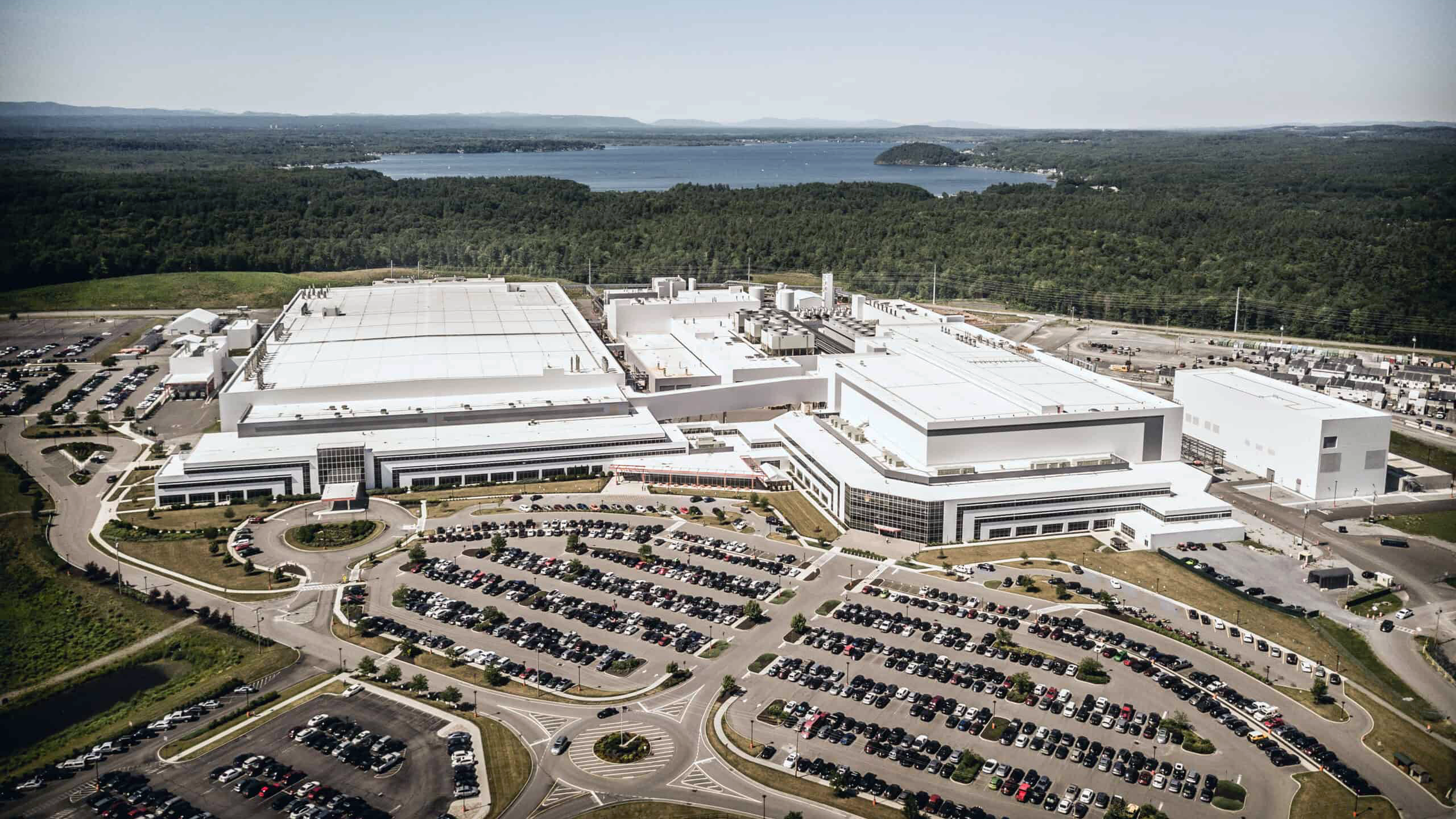
In addition, GlobalFoundries said it would build an all-new fab in Malta, New York, in a private-public partnership to support growing demand. The company hasn't revealed any information about this upcoming production facility, but given GlobalFoundries's focus on specialty nodes, expect the new chip plant to be aimed at various advanced specialty manufacturing technologies.
Recently Thomas Caulfield, chief executive of GlobalFoundries, said that GloFo would need financial support from the U.S. government provided under the CHIPS act to build and equip the new fab in New York quickly.
Samsung Foundry: SF's Leading-Edge Nodes Return to the U.S.
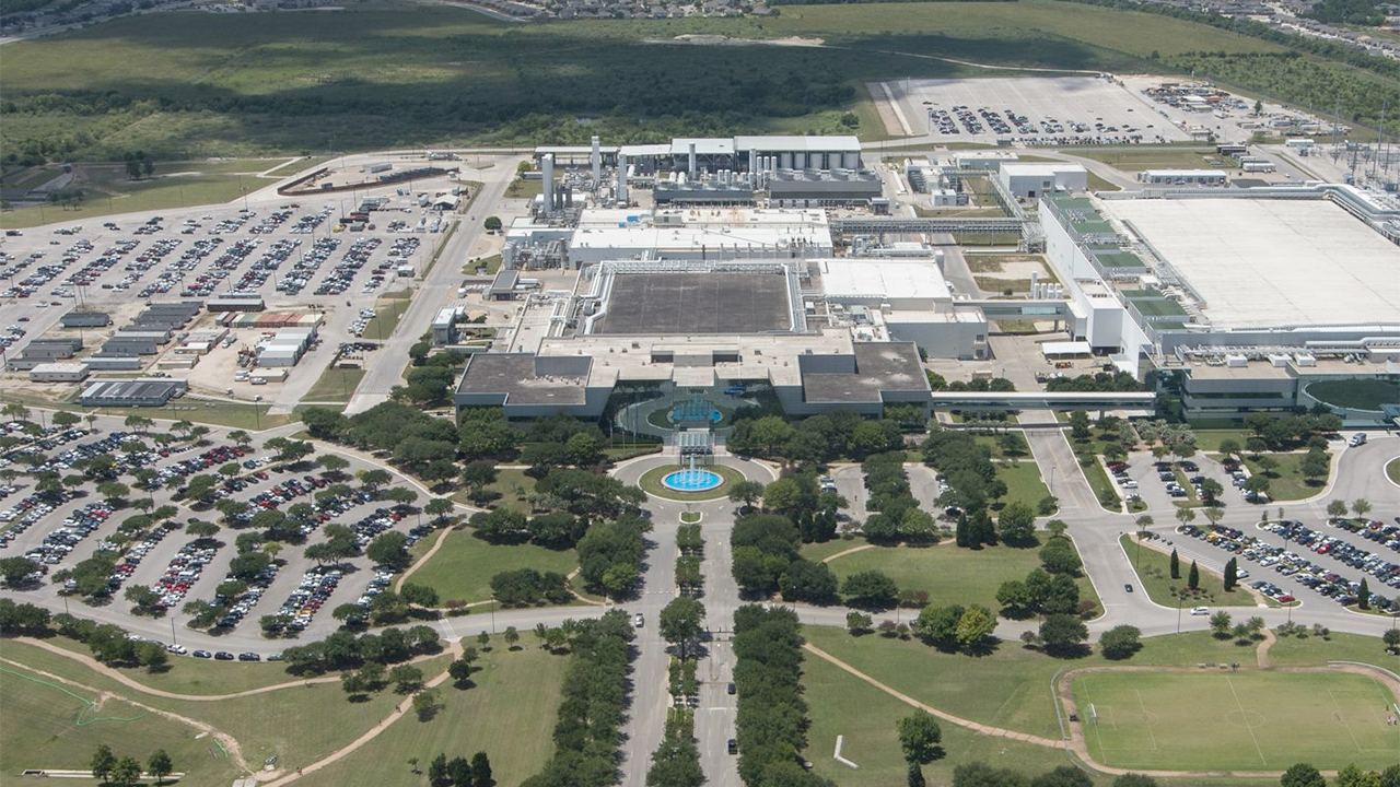
The Samsung Foundry division was quietly established in the U.S. in 2005 (with U.S.-based Qualcomm being the first customer). Since 2009, it has produced chips for Samsung and third-party customers in Austin, Texas.
Since Samsung was a part of IBM's common platform alliance (together with AMD/GlobalFoundries, Chartered, Freescale, and Infineon), at some point, it made sense for Samsung Foundry to produce chips using leading-edge technologies co-developed with its partners at its S2 plant in Austin, Texas. As a result, Samsung made its advanced 32nm, 28nm, and 14nm SoCs in Texas. In fact, cross-fab compatibility (and hence flexibility) between S2, S1 (Giheung, South Korea), and GF's Fab 8 provided Samsung with many advantages and put the Texas production facility in a unique position with its 14nm node.
Since IBM's fab club essentially ceased to exist and Samsung needed EUV lithography both for its DRAM and SoCs, it eventually moved its leading-edge node production to South Korea, leaving its S2 fab in Texas with older trailing nodes (14nm/11nm ~ 65nm). But Samsung still has many customers in the U.S. that need leading-edge nodes, so in late 2021 the company announced plans to build an all-new fab near Taylor, Texas. The project will cost $17 billion, and the new facility will come online in the second half of 2024.
Samsung hasn't formally disclosed which process technologies it will use at its new fab in Texas. Meanwhile, the company indicated that it would use the facility to manufacture chips for 5G, mobile, high-performance computing (HPC), and artificial intelligence (AI) applications starting in the second half of 2024. Timing and target applications clearly indicate that we are dealing with an advanced fab.
While this is pure speculation, we would expect Samsung to use its Taylor fab to produce chips on various 3nm-class fabrication nodes that rely on GAA transistors. As a result, Samsung will bring its leading-edge nodes back to Texas, which is good news for the company's customers in the U.S. and the country's semiconductor industry.
But Samsung Foundry apparently has big plans for Texas that span through 2042. The contract chipmaker recently filed 11 applications seeking tax breaks in Austin and Taylor for building new chip plants in the Manor and Taylor school districts. The total cost of the fabs is $192 billion (i.e., $17.5 billion per fab). The initial facilities will come online in 2034, whereas the remaining will start operations by 2042.
For now, the applications look like a means to secure incentives under the Chapter 313 incentives program that expires this year. Also, this is a good way to demonstrate to various authorities the intentions to invest in the U.S. semiconductor industry. Yet, these applications can hardly be considered even as optioned fabs as semiconductor fabrication facilities will cost significantly more in the looming High-NA EUV era.
Texas Instruments: $30 Billion for Specialty and Trailing Nodes
Although Texas Instruments is usually credited for inventing the microprocessor nearly simultaneously with Intel, the company has never become a supplier of general-purpose mass-market CPUs. It even wound down its OMAP mobile SoC business in 2012. But Texas Instruments is the world's largest maker of analog chips. For example, Apple's shiny new MacBook Pro comes with TI's audio amplifiers and USB-C power delivery controllers (these power controllers are used very widely these days). With a portfolio of over 45,000 products, Texas Instruments serves virtually all imaginable applications that need analog chips.
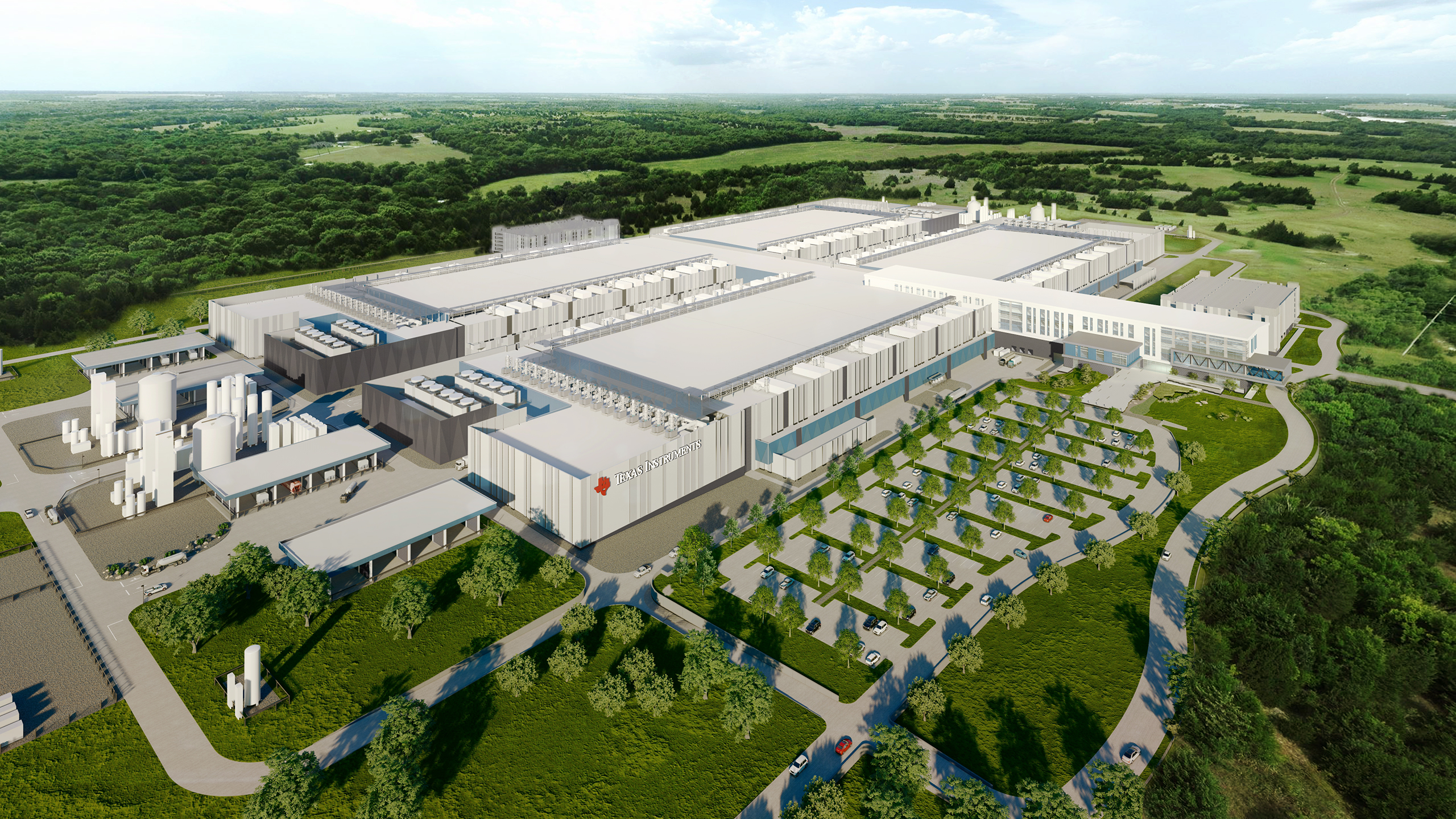
Texas Instruments runs its own fab as well as outsources some of the components it supplies. Like other chipmakers, TI faced unprecedented demand for its devices during the pandemic and is facing strong demand driven by contemporary industry megatrends (5G, AI, HPC, edge computing, autonomous vehicles). To meet the growing demand for its products, Texas Instruments started to build its new massive fab near Sherman, Texas, this May.
The new chip plant will be built in four phases, with the first fab coming online in 2025. The endeavor will be the largest economic project ever in Texas; it will cost TI about $30 billion and span a decade. Local authorities approved an incentive package that abates 90% of TI's property taxes for the fab's first 30 years to encourage TI to invest in Sherman and Grayson County.
There were other reasons why TI preferred Texas over other locations, though. The company already has three 300-mm semiconductor production facilities in the state (including DMOS6 in Dallas, RFab Phase 1 in Richardson, and the soon-to-be-completed RFab Phase 2 in Richardson), so it can share engineering talent between the sites. Furthermore, the company's suppliers are located locally too, so it will be easier to get materials and other goods for the new chip plant.
Summary
After years of stagnation, the U.S. is finally getting brand-new chip plants. Intel, GlobalFoundries, TSMC, and Samsung Foundry are set to spend well over $70 billion on U.S. fabs by 2025. If Texas Instruments's massive fab project (that comes online in 2025 and spans for several more years as new phases are built) and subsequent TSMC Fab 21 phases are added, we are looking at investments that might hit the $200 billion mark (or even exceed it) over the next decade.
To a large degree, such massive investments are made possible by several factors: incentive packages from local authorities, government subsidies enabled by the CHIPS act, availability of engineering talent, and the existing semiconductor production supply chain. Other reasons include geopolitical tensions and the necessity to diversify manufacturing bases.
The big question is whether the new American fabs are enough to compete against the massive upcoming Gigafab projects in South Korea and Taiwan. The answer isn't clear yet - new chip plants in the U.S. will build chips mostly developed in the U.S. and such centralization might bring some interesting rewards that we yet have to recognize. Meanwhile, the forthcoming fabs in Asia will produce chips designed in the U.S. and China, as South Korea and Taiwan (as countries) haven't yet developed their own chip designing capabilities.

Anton Shilov is a contributing writer at Tom’s Hardware. Over the past couple of decades, he has covered everything from CPUs and GPUs to supercomputers and from modern process technologies and latest fab tools to high-tech industry trends.
-
escksu Looking at the economy downturn and excess chips from Intel and Nvidia. I am not sure if this is a good thing.Reply -
Geef The need for chips will only increase. There are always good times and bad times for items but more and more people use tech that needs those chips. Don't think of only CPUs and Video Cards, consider every chip just in your kitchen. Microwave, Refrigerator, Stove, Blender. The list goes on and thats just a few items in a kitchen. :geek:Reply -
Pei-chen Let’s pretend TSMC and Samsung really want to bring their country’s most valuable technology leads to the US;)Reply -
Kahless01 Reply
you left out the $80 billion+ 11 building campus Micron is wanting to build in Lockhart tx. the locals are fighting it because they dont wanna become a big city. but since this is texas the government will always let businesses come in.Admin said:Intel, GlobalFoundries, Samsung Foundry, TI, and TSMC are building new fabs in the U.S. Here's everything we know about the upcoming facilities.
U.S. Semiconductor Renaissance: All the Upcoming Fabs : Read more -
Geef ReplyPei-chen said:Let’s pretend TSMC and Samsung really want to bring their country’s most valuable technology leads to the US;)
If China invades Taiwan I have a feeling there will be a LOT of TSMC employees who will immigrate to America. Having a place to immediately get to work would really help. -
Why_Me Reply
Let's pretend China isn't threatening Taiwan's sovereign status.Pei-chen said:Let’s pretend TSMC and Samsung really want to bring their country’s most valuable technology leads to the US;)

