Intel to Make Custom x86 CPUs as Part of Ambitious Expansion Plan
Intel will keep its fabs, outsource some of its products, produce chips for others.
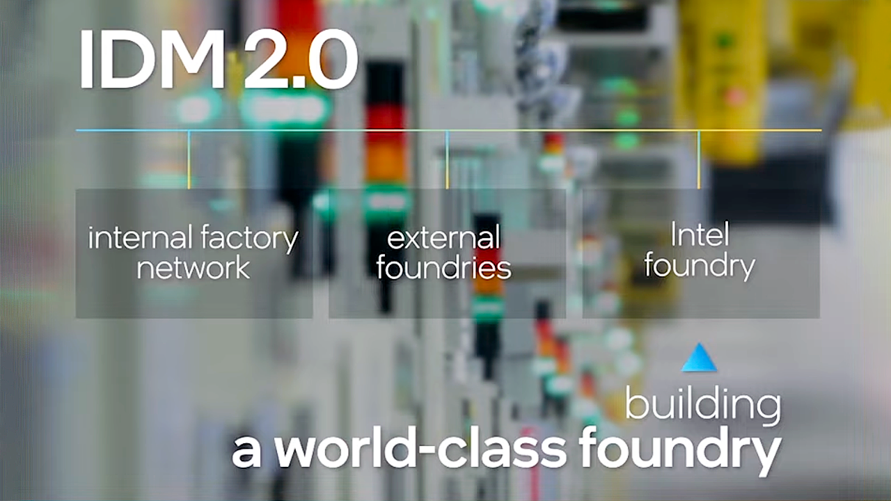
Intel on Tuesday revealed its vision for the future called IDM 2.0, which is an evolution of the company's integrated device manufacturing (IDM) model mixed with two contrasting ingredients: outsourcing and foundry services.
Intel will not give up its own manufacturing and will do everything it needs to recapture process technology leadership. Furthermore, Intel will build additional production capacities in the U.S. and Europe and will start offering foundry services to third parties. The company will spend $20 billion to expand its capacities in Arizona.
To gain customers, Intel Foundry Services will offer clients Intel's IP, including customizable CPU cores, and will embrace industry-standard IP and flows, making it relatively easy to switch from other makers to Intel. Imagine an Amazon, Microsoft or Google-designed x86 chip! Meanwhile, to offer its customers absolutely the best products, Intel will outsource some of its devices to third parties that happen to have something that Intel does not.
Regaining Process Technology Leadership
Intel was late to market with its 10 nm fabrication process and while this node proves to be competitive against TSMC's N7 as far as the combination of performance, power, and transistor density is concerned, TSMC's N5 and Samsung's 5LPE technologies clearly offer lower power and better density.
The 10 nm delay is nothing good, but such things happen with IDMs without causing major problems. What is particularly bad for Intel is that Samsung Foundry and TSMC are gaining experience with extreme ultraviolet (EUV) lithography in high volume manufacturing (HVM) while the CPU giant is fixing yields at 10 nm fabs and redeveloping its 7 nm node in the lab.
A redesign is indeed what Intel has done with its 7 nm fabrication process. Pat Gelsinger, Intel's new CEO said that when Intel started to develop its 7 nm technology, it was not sure it could extensively use EUV tools, so it sticked to multi patterning techniques. Things like quad, penta, or hexa-layer patterning already affected defect density at 10 nm and forced Intel to redesign the node. At 7 nm, multi patterning naturally causes even more negative effects than it does on 10 nm, which is why the company eventually found defect density of its initial 7 nm technology too high.
As a result, the manufacturer had to redesign the process, increase usage of EUV tools by two times (i.e., use it for 2X more layers), and simplify design rules, which will be good for yields, cycle times, and costs. Unfortunately, Intel does not share characteristics of its new 7 nm fabrication process and how it stacks up against its 10 nm SuperFin and 10 nm Enhanced SuperFin technologies.
Get Tom's Hardware's best news and in-depth reviews, straight to your inbox.
In general, the good news is that Intel is finally happy with its 7 nm EUV-based technology and is on track to tape in one of its 7 nm designs — CPU tile of the codenamed Meteor Lake product — in Q2 2021. If everything goes well, Meteor Lake will hit the market sometimes in 2023. Meanwhile, it looks like GPU compute slice for Intel's codenamed Ponte Vecchio processor for supercomputers will have to be made at TSMC for quite a while as the product has to ship in 2022.
Many observers note that one of the reasons why Intel's 10 nm technology suffered too high defect density initially were too-aggressive design goals. Having learned its lessons with its 10 nm process, Intel has adopted a foundry-like iterative node development model that is rather cautious and is made to reduce risks.
Starting from 2019, Intel introduced a new version of its 10 nm technology every year with some improvements. Each new iteration does not have to bring a huge set of improvements, but it enables the company to build competitive products. The company will follow the same tactics going forward, according to Pat Gelsinger, chief executive of Intel. Such an approach will be beneficial not only for Intel itself, but also for its foundry customers.
As far as products are concerned, Intel is predicting 'unquestioned' CPU performance leadership in the 2024 – 2025 timeframe. Meanwhile, the company says nothing particular about when it plans to regain process technology leadership.
Since Intel's 7 nm is on track for 2023, it will compete against TSMC's N3 (3 nm, FinFET) and Samsung's 3GAE (3 nm, MBFCFET) nodes. Analysts from China Renaissance Securities modeled that if Intel can realize full node PPA (power, performance, area) gains transiting from 10 nm to 7 nm, then its next-gen technology's transistor density will be between 230 MTr/inch2 and 240 MTr/inch2.
Meanwhile, the transistor density of TSMC's N3 is projected to be in the range of 250 MTr/inch2, whereas Samsung Foundry's 3GAE's transistor density is projected to be slightly below 220 MTr/inch2. These numbers are very rough estimates, so it is hard to draw many conclusions based on them. Still, it does not look like Intel could have the industry's best fabrication process with its 7 nm in 2023.
Research Collaboration with IBM
In order to be a successful maker of its own products and offer competitive foundry services, Intel will have to offer a portfolio of comprehensive process technologies and be able to produce chips in high volume. Developing of modern semiconductor fabrication processes is already very expensive as it requires extensive fundamental research of materials and transistor structures.
In a bid to strengthen its research organization and share costs, Intel signed a deal with IBM regarding joint research of upcoming fabrication processes as well as advanced packaging technologies, two things that are fundamental to the future of semiconductor manufacturing in the coming years.
The two companies did not elaborate on what are they going to research and develop together and the press statement reading that they "aim to accelerate semiconductor manufacturing innovation, enhance the competitiveness of the U.S. semiconductor industry and support key U.S. government initiatives" does not really tell a lot. But perhaps the key message here is that Intel is now willing to work with industry peers rather than research and develop everything in house.
New Fabs in the U.S. and Europe
Intel Foundry Services (IFS) is not Intel's first attempt to enter the foundry business. Intel used to have its Intel Custom Foundry (ICF) division several years ago, but it never really took off mainly because Intel did not really need it at the time. Today, Intel needs to increase the scale of its semiconductor manufacturing beyond its own products due to increasing R&D costs, increasing costs of tools, and rising operational costs (consumables, parts, etc. are getting more expensive). To that end, Intel needs IFS to be competitive.
Intel Foundry Services will be a separate company within Intel that will be led by semiconductor industry veteran Dr. Randhir Thakur, who will report directly to Pat Gelsinger. IFS will be focused primarily on advanced technologies and will use not only Intel's existing fabs, but will also add new capacities specifically built for the foundry operations. Just like foundries like TSMC, IFS will offer industry-standard process development kits (PDKs) containing building blocks and design rules. It will also embrace industry-standard electronic design automation (EDA) tools from Cadence and Synopsys that fabless developers of chips use. By contrast, neither PDKs nor standard EDA tools were ever made available to ICF customers years ago, so Intel is fixing this with IFS.
To enable its large-scale foundry operation in the U.S., Intel is set to build two new EUV-capable fabs in Arizona, located at the company’s Ocotillo campus near other fabs that make Intel's products for existing customers. Intel will begin construction of the new fabs this year and will spend about $20 billion on them, which suggests that these are not going to be very large fabs. The State of Arizona as well as the U.S. government are set to provide a set of incentives for Intel to build these fabs, the company said without elaborating.
Going forward, Intel plans to build additional fabs for its own products and the IFS division particularly in the U.S., Europe, and other locations. The appropriate announcements are expected within 2021. The company is not yet ready to disclose exact plans as it is probably considering various options, but it is evident that the firm wants to offer its foundry services globally.
Unlike with traditional foundries, Intel does not seem to be interested in legacy nodes and wants to make chips using lucrative advanced fabrication technologies. Meanwhile, as the company is working to become one of the U.S. Department of Defense's primary foundries, it will have to keep outdated fabs afloat for quite a while.
Bringing 7 nm to Europe
As a part of its ongoing effort to spread its production capacities across the globe, Intel has invested an additional $7 billion from 2019 to 2021 in an ongoing expansion of its Ireland fab. The upgrade will install EUV tools into the production facility and will make it capable of producing chips using Intel's 7 nm node, essentially bringing a leading-edge 7 nm technology to Europe in the coming years. But there is a catch.
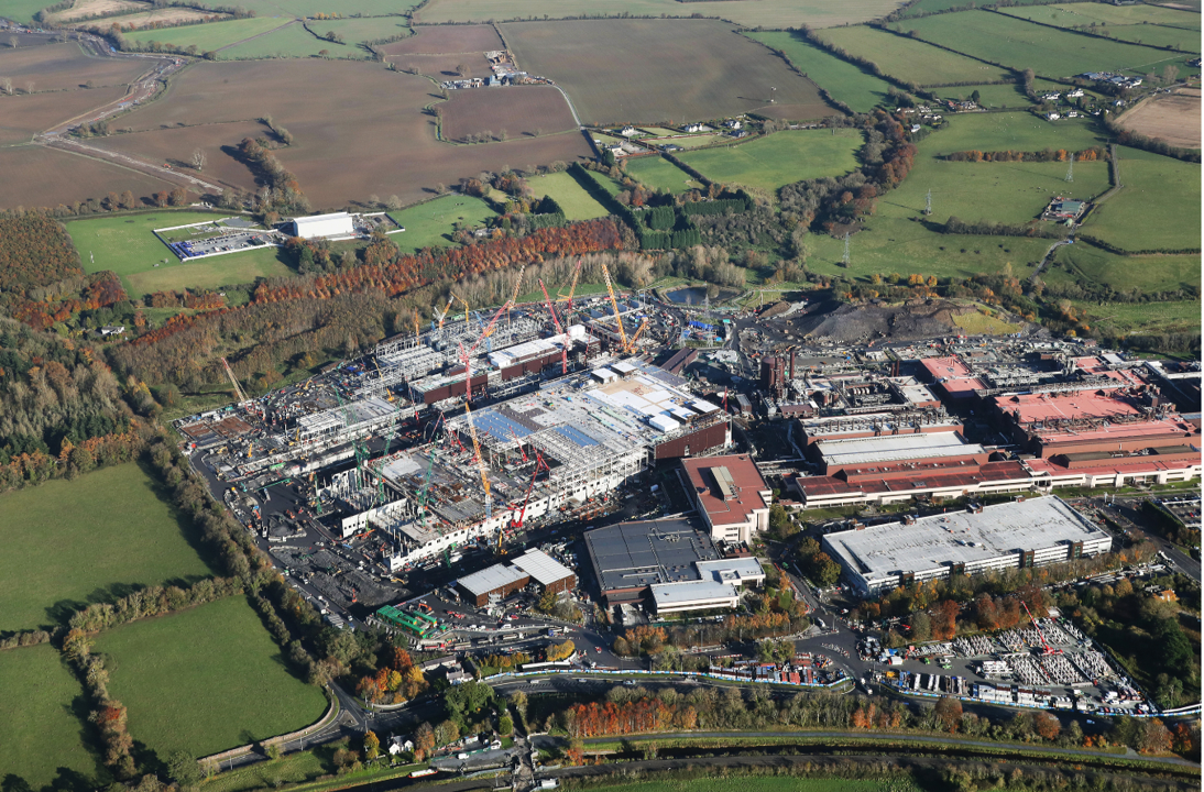
As Pat Gelsinger told the news conference this week, the company plans to announce the next phase of expansions to support the company's new foundry business in the USA, Europe and other global locations within the year, so Intel might be bringing more EUV-capable capacities to Europe, well ahead of other foundries, which might be offered an opportunity by the EU authorities.
Intel yet has to reveal particular details about its foundry efforts in Europe, but it is evident that the chip giant is very serious about making advanced chips on this side of the pond.
Intel's IFS: Agnostic to Architectures, But with Unique Propositions
Contract production of semiconductors has many ingredients. Production capacities and process technologies are two corner stones of any chipmaking operation. Foundries also need to ensure that they have decent PDKs, simple design rules, compatibility with industry-standard design tools, and a portfolio of foundational IP that further simplifies chip development. To make IFS a world-class foundry Intel plans to invest in an IP portfolio that will include standard interfaces, third-part IP building blocks, and Intel's own IP blocks.
As a foundry, Intel's IFS will be agnostic to chips and architectures it produces. The company has no problems making SoCs based on Arm or RISC-V CPU cores and featuring graphics by Arm or Imagination Technologies, just like any other contract maker of semiconductors. But IFS will have two important advantages over its industry peers as its customers will have access to Intel's IP and packaging technologies.
Nowadays the majority of system-on-chips are designed by developing and implementing differentiating IP or IPs, then throwing-in a defined Arm core developed by Arm, memory and storage controllers as well as appropriate physical interfaces developed by another supplier as well as various necessary IP blocks. Instead of using Arm, RISC-V, or PowerVR, IFS customers will be able to opt for Intel's x86 CPU, Xe GPU, media, graphics, fabric, and other critical IP. Of course, they will have to pay a license fee and agree to certain terms, but in a nutshell, IFS could build custom x86 processors that will rival those from Intel.
Of course, the vast majority of IFS's customers will stick to industry-standard IP for many reasons (competing with Intel on its own field might not be a good idea), but an ability to license Intel's IP cores may be plausible for at least some companies. For example, building a custom SoC with Intel's market-leading media encoders/decoders as well as graphics IP might be an interesting option for various cloud gaming companies. Also, exascalers like Microsoft or Google could design their own x86-based datacenter SoCs. Given how complex modern SoCs may be, Intel's HVM-proven EMIB and Foveros technologies will be extremely important for customers looking to build something very small (like Intel's Lakefield) or very big (like Intel's Ponte Vecchio).
In fact, there are a number of companies that Intel said were excited about establishment of IFS and opportunities it provides, including Amazon, Ericssson, Google, Microsoft, and Qualcomm. While certainly these companies do not commit to use Intel's foundry services, even endorsing IFS is a good start for the operation.
Summary
For most of its 52-year history, Intel has been an integrated device manufacturer of CPUs. In the last 20 years Intel's products portfolio expanded rather significantly and in the most recent years Intel began its foray into GPUs, FPGAs, and XPUs. Last year the company started a major effort to re-invent itself and its approach to product design. The newly announced IDM 2.0 strategy is a yet another step in the direction towards the new Intel.
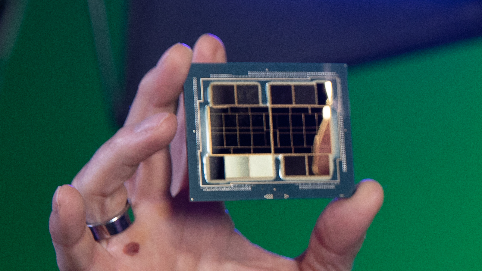
A modular approach to chip design enables Intel to make chiplets or tiles for its products using different process technologies at different fabs internally and externally, so in 2023, the company is going to take advantage of this by outsourcing some of its products to TSMC. Even before that, it will release its codenamed Ponte Vecchio compute GPU that will be produced using a variety of fabrication processes and will contain building blocks by Intel, TSMC, and Samsung Foundry.
At the same time, Intel's decision to enter contract semiconductor production business indicates that the company is confident of its ability to offer the best node in the future. Meanwhile, Intel needs its IFS business in a bid to stay on par with TSMC and Samsung Semiconductor in terms of scale.
For now, there are more questions than answers about Intel's strategy for IFS as so far, the company has only announced intentions to build additional capacities around the globe and that it was interested primarily in lucrative advanced manufacturing technologies. Meanwhile, it is unclear how often Intel will be able to upgrade its fabs if it has long-term supply contracts with clients like the U.S. DoD.

Anton Shilov is a contributing writer at Tom’s Hardware. Over the past couple of decades, he has covered everything from CPUs and GPUs to supercomputers and from modern process technologies and latest fab tools to high-tech industry trends.
-
dave.jeffers The ship has been floundering for years now. The Lieutenant has been promoted to Captain, and is now saying whatever it takes to calm the crew and passengers. But make no mistake, the ship is sinking.Reply -
spongiemaster Reply
AMD was practically bankrupt before Ryzen launched. Intel replaced their CEO 2 months ago. AMD didn't turn it around that quickly, and Intel isn't starting from nearly the dire position that AMD was in. We won't know for a couple years if Intel is in a death spiral or if they've gotten back on track.dave.jeffers said:The ship has been floundering for years now. The Lieutenant has been promoted to Captain, and is now saying whatever it takes to calm the crew and passengers. But make no mistake, the ship is sinking. -
atomicWAR Replydave.jeffers said:The ship has been floundering for years now. The Lieutenant has been promoted to Captain, and is now saying whatever it takes to calm the crew and passengers. But make no mistake, the ship is sinking.
Hardly, this isn't the first time AMD has knocked Intel off balance. AMD64 CPUs thoroughly creamed Intel's Pentium 4 and Pentium D processors when they launched. That situation was even worse than now for Intel. Intel can at least compete as of now even if they don't have the advantage unlike when AMD64 launched. Regardless Intel still has loads of money to throw at the problem and the engineering talent to make it happen. Plus when you look at the Alder Lake launch, that will be the first Keller designed architecture...you know the guy who designed Zen. So until Intel cash reserves are toast and they've lost the server/data center market, the fight is far from over. Besides the last thing any enthusiast should want is for an x86 maker to go under. If we lose Intel, we lose competition and we'll be in a worse boat than the early Intel Core days when AMD Faildozer...I mean bulldozer just couldn't keep up and AMD stock price was in the trash can. -
jkflipflop98 Replydave.jeffers said:The ship has been floundering for years now. The Lieutenant has been promoted to Captain, and is now saying whatever it takes to calm the crew and passengers. But make no mistake, the ship is sinking.
LOL no. -
hotaru.hino Reply
Adding to everything said above, Intel is more than a CPU manufacturing company. They have their hands in plenty of other products that are doing just fine. This is on top of Intel's net income is still an order of magnitude higher than AMD's.dave.jeffers said:The ship has been floundering for years now. The Lieutenant has been promoted to Captain, and is now saying whatever it takes to calm the crew and passengers. But make no mistake, the ship is sinking. -
JasHod1 The article says that they would custom design x86 with other customers but not x64. As x64 is a AMD design which AMD cross licenses with Intel exclusively for their use (not to be fabbed or designed for other companies) and most programs are now written and run in x64, what use is this announcement?Reply -
JayNor "Still, it does not look like Intel could have the industry's best fabrication process with its 7 nm in 2023."Reply
Intel has the combination of Foveros, EMIB, silicon photonics, PAM4 technology, CXL, Optane, FPGAs.
The xe-hpc chip that the CEO held up ... if it works ... will certainly make their point. -
TerryLaze Reply
It's AMD that should be scared to death right now, if intel can supply GPUs all year around instead of only around release date it's going to be a really bad time for AMD, and nvidia to a somewhat smaller degree.spongiemaster said:AMD was practically bankrupt before Ryzen launched. Intel replaced their CEO 2 months ago. AMD didn't turn it around that quickly, and Intel isn't starting from nearly the dire position that AMD was in. We won't know for a couple years if Intel is in a death spiral or if they've gotten back on track.
If intel decides to make super cheap CPUs with a big XE chip in it and offer them to MS and Sony in "unlimited" supply it's going to be an even worse time for AMD.
What do you mean, the other thing besides x64 is x32 (64 bit and 32 bit) they both run on x86 technology.JasHod1 said:The article says that they would custom design x86 with other customers but not x64. As x64 is a AMD design which AMD cross licenses with Intel exclusively for their use (not to be fabbed or designed for other companies) and most programs are now written and run in x64, what use is this announcement? -
JasHod1 ReplyTerryLaze said:It's AMD that should be scared to death right now, if intel can supply GPUs all year around instead of only around release date it's going to be a really bad time for AMD, and nvidia to a somewhat smaller degree.
If intel decides to make super cheap CPUs with a big XE chip in it and offer them to MS and Sony in "unlimited" supply it's going to be an even worse time for AMD.
What do you mean, the other thing besides x64 is x32 (64 bit and 32 bit) they both run on x86 technology.
Intel licence x64, the 64 bit extensions, from AMD. AMD made that extension to x86. That would not be covered by this agreement. Intel can make and fab a plain x86 processor for anyone they like but not with the x64 extensions, they're AMD's. They do not run on x86, try running x64 on any Intel processor before a Pentium 4. -
ekio It's so annoying to see those companies trying to force the obsolete x86 to continue its painful existence, instead of providing the world with newer high quality ISAs like RISC-V....Reply
