Intel’s Long Awaited Fab 42 is Fully Operational
Intel’s Fab 42 joins fleet of Intel’s 10nm production facilities
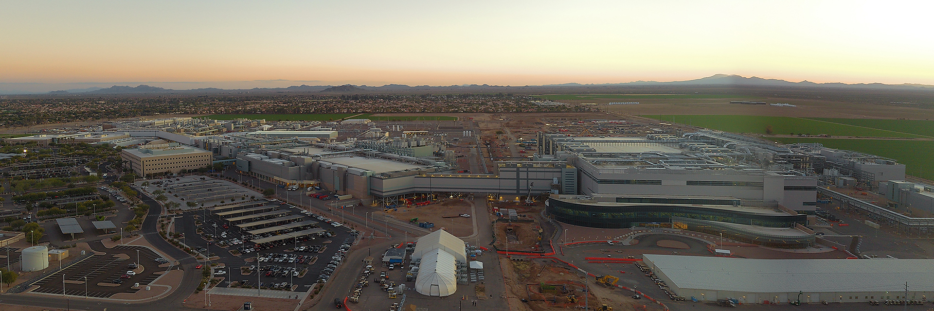
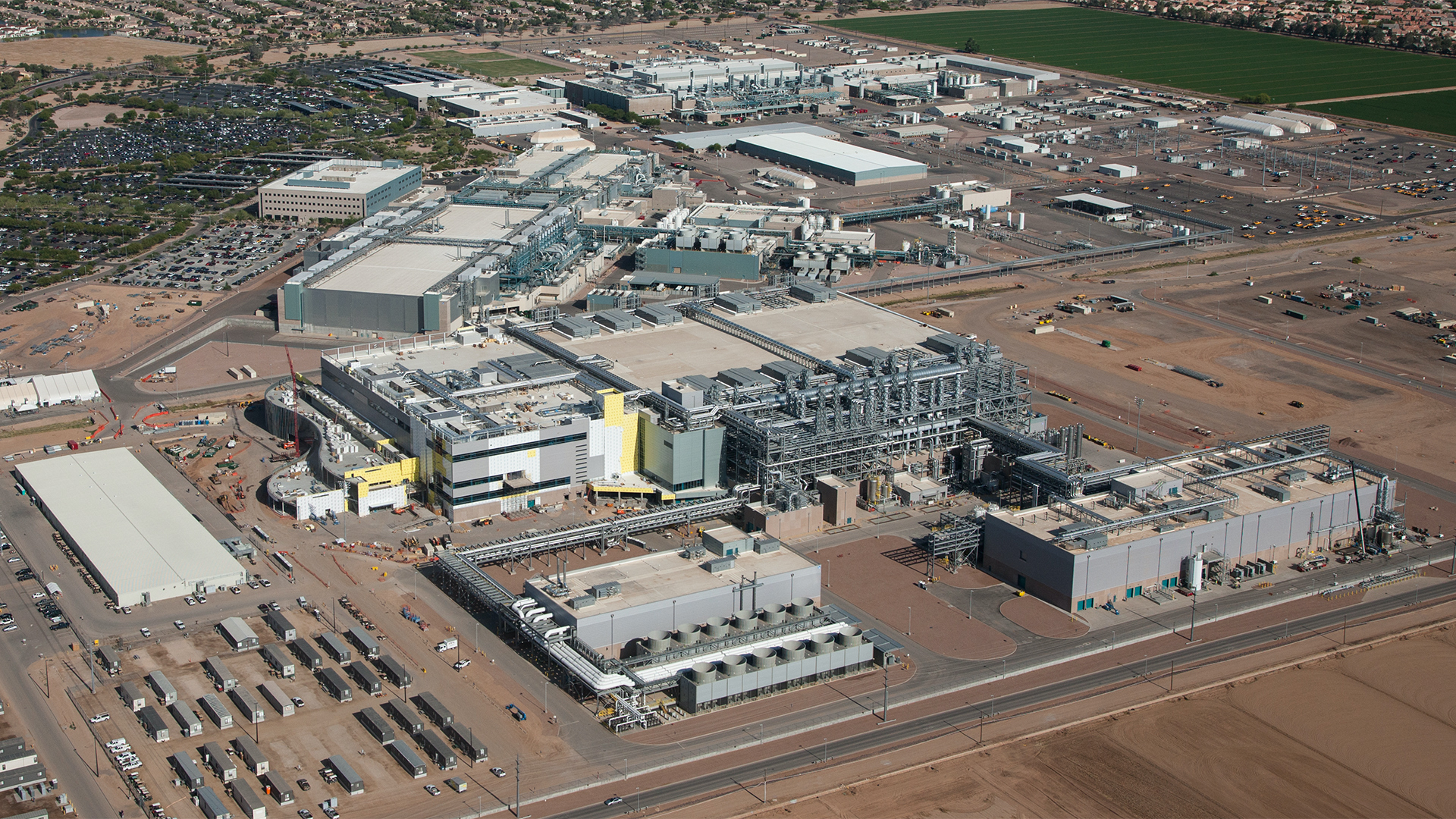
Intel last week said that its Fab 42, which began construction in 2011, had started operations. The manufacturing facility is producing processors using the company’s 10nm process technology and is the company’s third location to use the company’s latest node. The addition of the third 10nm capable fab to the fleet can significantly improve availability of Intel’s latest products. (Via AZCentral/Intel)
The Third 10nm Fab
Intel can produce chips using its 10 nm process technologies (2nd generation 10nm used for Ice Lake, Ice Lake-SP, Elkhart Lake, Snow Ridge as well as 3rd generation 10nm SuperFin used for Tiger Lake and DG1) at three of its sites: in Israel, Oregon, and Arizona. All of the company’s 10nm products released to date were produced either in Oregon or in Israel as Fab 42 in Arizona was waiting for demand for 10nm CPUs to pick up.
The addition of Fab 42 to the fleet of facilities that manufacture 10nm products in high volume promises to significantly improve Intel’s abilities to supply said processors. As a result, there will be more Tiger Lake-based designs when compared to Ice Lake-powered designs.
Intel traditionally does not disclose production capacity of its fabs, but it noted that Fab 42 connects to three other Intel fabs, making the site the company’s ‘first mega-factory network.’ Typically, megafabs are fabrication facilities that offer capacity between 25,000 and 100,000 wafer starts per month. Meanwhile, WSPM capacity depends on particular process technology and varies between nodes.
According to Intel, so far it has invested over $23 billion on its manufacturing facility in Arizona. At present, it employs 12,000 people in the state.
Intel’s Fab 42: A Short History Lesson
Intel’s Fab 42 has an interesting history as one of the company’s leading-edge manufacturing facilities. The world’s largest maker of processors started to construct the factory in 2011. Back then the prospects of extreme ultraviolet (EUV) lithography were uncertain, so Intel envisioned that the industry might move to larger — 450mm — wafers in the foreseeable future. As a result, Fab 42 was built to be compatible with equipment processing 450mm wafers.
The construction was completed in 2013 and essential things like heating and air conditioning were installed. But in early 2014 the company decided not to move in semiconductor production equipment used to make chips using then leading edge 14nm process technology as it was not sure about demand.
Get Tom's Hardware's best news and in-depth reviews, straight to your inbox.
In early 2017, Intel announced plans to spend $7 billion to equip its Fab 42 in a bid to make chips using its next-generation 7nm fabrication technology. Over time it turned out that Intel needed more 10nm capacity, so the fab was equipped with tools required for 10nm nodes that are supposed to use the same production equipment. Meanwhile, it is unclear whether Fab 42 can indeed produce chips using Intel’s 7nm manufacturing process that relies both on DUV and EUV lithography.

Anton Shilov is a contributing writer at Tom’s Hardware. Over the past couple of decades, he has covered everything from CPUs and GPUs to supercomputers and from modern process technologies and latest fab tools to high-tech industry trends.
-
spongiemaster ReplyAll of the company’s 10nm products released to date were produced either in Oregon or in Israel as Fab 42 in Arizona was waiting for demand for 10nm CPUs to pick up.
Not sure about that one, unless you mean demand from Intel themselves as in having a functional product to produce at the fab. -
InvalidError That will hopefully be enough to move most remaining laptop chip production to 10nm and free up some 14nm to catch up on the backlog there.Reply -
digitalgriffin ReplyInvalidError said:That will hopefully be enough to move most remaining laptop chip production to 10nm and free up some 14nm to catch up on the backlog there.
If Intel doesn't hurry and get a competitive desktop part out soon (Rocket lake), 14nm supply really won't be an issue. Trends indicate a downward movement of sales now the back to school laptop rush is over. -
TerryLaze Reply
Which year do you live in?digitalgriffin said:If Intel doesn't hurry and get a competitive desktop part out soon (Rocket lake), 14nm supply really won't be an issue. Trends indicate a downward movement of sales now the back to school laptop rush is over.
Back to school sales?! Sales have been crazy since the start of the year due to the human malware.
If you have a specific link that you got that idea from please link it here,I'm very curious to read that. -
digitalgriffin ReplyTerryLaze said:Which year do you live in?
Back to school sales?! Sales have been crazy since the start of the year due to the human malware.
If you have a specific link that you got that idea from please link it here,I'm very curious to read that.
Some schools quit the school year early to avoid at home teaching.
There was a second rush at the beginning of the new school year.
While its not quantitative, I have a number of friends on facebook who are getting new laptops. Schools are ramping up with new curriculum and software packages for teaching and parents are discovering their old equipment isnt up to snuff. A visit to my local best buy and walmart also shows just about every laptop sold out. But im seeing increased availability online finally. -
neojack this new facility would be even nicier with some blue solar panels on the roof.Reply
because , you know... Arizona...
plus it's good advertizing (well maybe not in the southern US because they prefer to burn coal for some reason) -
cryoburner Reply
The coronavirus mitigations may have significantly boosted computer hardware sales this year, but how long do you expect that to last? Most of those who decided to buy a new system as a result of the pandemic have likely already done so by this point. And once someone has a new system, they probably won't be buying a replacement for some years to come. So, in many cases, they have effectively moved up a purchase of new hardware to an earlier date, and as a result, there will likely be a dropoff in demand before long. While 2020 sales may have been notably higher than expected, 2021 sales could easily be lower.TerryLaze said:Which year do you live in?
Back to school sales?! Sales have been crazy since the start of the year due to the human malware.
If you have a specific link that you got that idea from please link it here,I'm very curious to read that.
The majority of those getting a new system for working at home probably did so back in the spring or early summer. Those getting one for school have probably done so already as well. There will likely continue to be decent sales numbers through the holiday shopping season, but after that, we may see somewhat of a downturn in sales. I suppose if there happens to be an increase in businesses and schools shutting down during the flu season we could see strong sales continue for some time, but with more precautions being taken to to reduce transmission this time around, it seems likely that we probably won't see a similar situation as there was last spring.
I can't really see Intel "hurrying" to get Rocket Lake out there, since they just released their Comet Lake desktop processors several months back. And realistically, those processors are relatively competitive. They finally more or less roughly match AMD in terms of thread counts in most product segments, and while the higher-end unlocked parts still cost more, they do offer a bit more lightly-threaded performance. That might potentially change once AMD launches their new generation of processors though. Of course, we don't even know if Rocket Lake will be a notable step up over their existing offerings. Either way, I wouldn't expect them before the first quarter of next year, at the earliest, and it could be later.digitalgriffin said:If Intel doesn't hurry and get a competitive desktop part out soon (Rocket lake), 14nm supply really won't be an issue. Trends indicate a downward movement of sales now the back to school laptop rush is over. -
shady28 Replycryoburner said:The coronavirus mitigations may have significantly boosted computer hardware sales this year, but how long do you expect that to last? Most of those who decided to buy a new system as a result of the pandemic have likely already done so by this point. And once someone has a new system, they probably won't be buying a replacement for some years to come. So, in many cases, they have effectively moved up a purchase of new hardware to an earlier date, and as a result, there will likely be a dropoff in demand before long. ,,,
Well, I don't think anyone knows, and if they do know for sure how it will play out they should be finding some beat up small cap PC stocks to buy, or to short, for whatever the scenario may be.
As for myself, a software engineer, I built a PC for the first time in 10 years back in June/July. I had stopped building but bought new every 3 years. My personal laptop started to fall apart after 3 months of WFH.
Actually so has my work laptop, so I'll be getting a new one soon. I also just bought a 34" 100Hz UW 3440x1440 monitor. And about $250 into mouse and keyboard. Also a 3TB USB 3.1 backup drive. And a UPS after a few power outages.
Oh and I was rather quick to upgrade my stuff. I know a lot of people, developers, who are starting to think about it now. A lot of people are upgrading things other than their PCs, but there are some who are upgrading because MS Teams can bring a haswell gen laptop to its knees.
IMO, we will continue to see sustained demand for PCs and peripherals through the end of the year.
After that, like pretty much every other sector of the economy, it's going to depend on if the economy can really recover. If all these failed businesses get replaced with startups and companies that have done massive permanent layoffs start to come back, PC demand will boom.
If it starts to spiral down, and it may well do that, then how to save money by reducing the amount of water your toilet bowl uses by displacing it with a 2 liter soda bottle will probably be a more important topic.

