Japanese scientists develop simplified EUV scanner that can make production of chips considerably cheaper
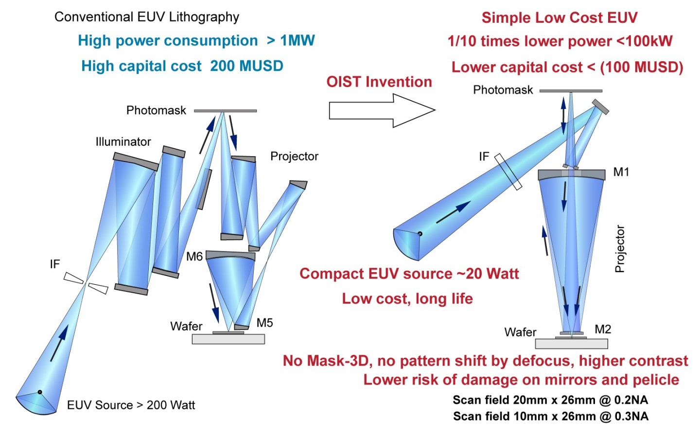
OIST's simplified EUV litho system uses two mirrors instead of six.

Professor Tsumoru Shintake of the Okinawa Institute of Science and Technology (OIST) has proposed an all-new and greatly simplified EUV lithography tool that is cheaper than those developed and made by ASML. If the device hits mass production, it could reshape the chipmaking equipment industry, if not the whole semiconductor industry.
The new system uses only two mirrors in its optical projection setup, a significant departure from the conventional six-mirror configuration. The challenge of such an optical system is that it involves aligning these mirrors in a straight line, which ensures that the system maintains high optical performance without the usual distortions associated with EUV light. The new optical path allows more than 10% of the initial EUV energy to reach the wafer, compared to about 1% in standard setups, an improvement which is a major breakthrough.

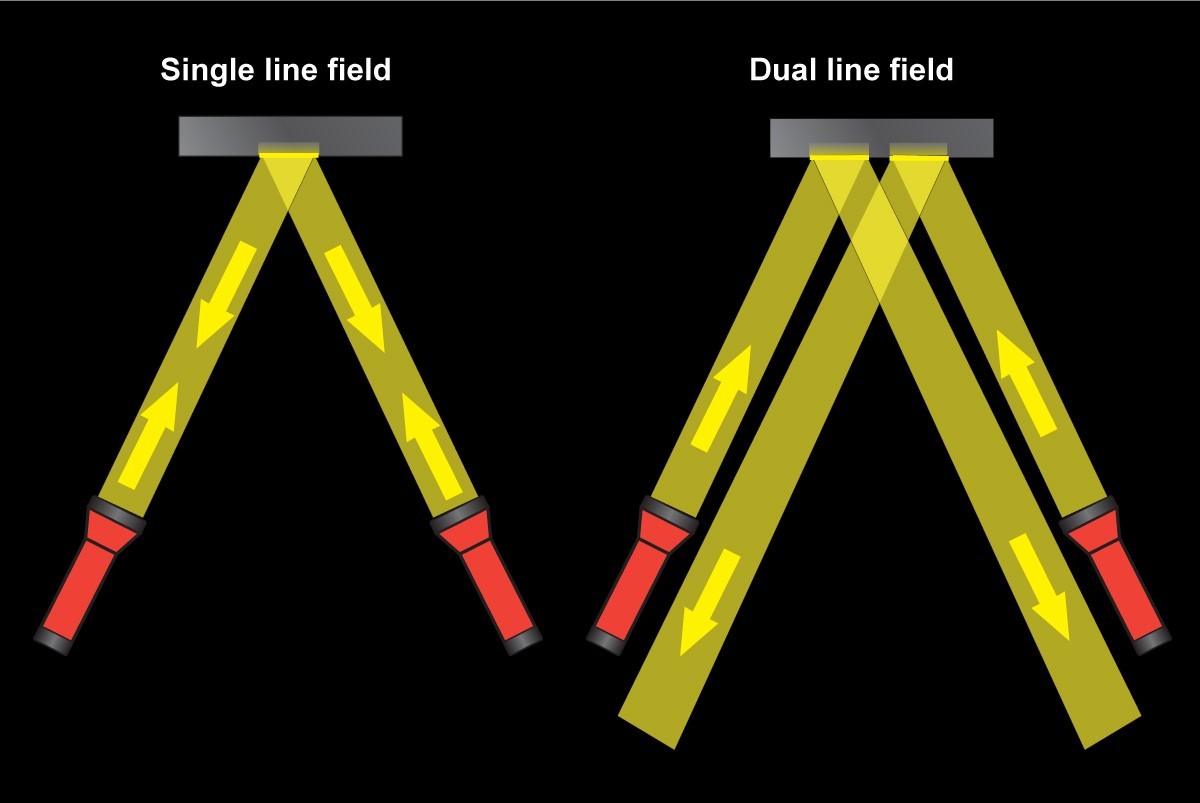
Professor Shintake's team solved two major challenges in EUV lithography: preventing optical aberrations and ensuring efficient light transfer. OIST's 'dual-line field' method illuminates the photomask without interfering with the optical path, which minimizes distortions and enhances image precision on the silicon wafer.
One of the key advantages of this minimalist design is that it enhances reliability and reduces maintenance complexities. Another advantage of this EUV lithography tool design is a drastic reduction of its power consumption. Thanks to the optimized optical path, the system operates with an EUV light source of just 20W, leading to a total power consumption of less than 100kW. In contrast, traditional EUV lithography systems often require over 1MW of power. Because of lower power consumption, the new litho system does not require a sophisticated and expensive cooling system.

The performance of this new system has been rigorously verified using optical simulation software, confirming its capability for producing advanced semiconductors. The technology's potential has led to a patent filing by OIST, indicating readiness for commercial deployment.
OIST is committed to advancing its EUV tool design further, aiming to bring it to practical application. The institute sees this innovation as a vital step toward solving global challenges, such as the costs of chip production and power consumption of semiconductor fabs, which affect the environment.
The economic implications of this invention are promising. The global EUV lithography market is expected to grow from $8.9 billion in 2024 to $17.4 billion by 2030. With this simplified design of EUV tools, the industry could adopt more EUV systems in the coming years. However, it is unclear how close OIST is to commercialization of its tool.
Get Tom's Hardware's best news and in-depth reviews, straight to your inbox.

Anton Shilov is a contributing writer at Tom’s Hardware. Over the past couple of decades, he has covered everything from CPUs and GPUs to supercomputers and from modern process technologies and latest fab tools to high-tech industry trends.
-
edzieba Reading the paper, this comes with a few heavy caveats:Reply
- only 0.2 NA, with a 0.3 NA version being proposed but requires a curved surface photomask to be fabricated (not a trivial task). High-NA EUV is 0.5 NA, and 'standard' EUV is 0.33 NA.
- 10m x 26mm field size. Even the 'small' field of TSMV's high-NA EUV machines is 16.5x26, and 'standard' EUV is 33x26mm.
- all-aspheric optics
- has not been tested in a physical system
So the technique is both lower resolution than both standard and high-NA EUV, a much smaller reticule size than even high-NA EUV, and may require custom 2D curved masks and pellicles requiring new fabrication techniques compared to existing masks and pellicles (as if EUV pellicles weren't already enough of an issue).. It also requires fabrication of perforated aspheric Bragg mirrors, which is nontrivial. -
dehjomz So should ASML be worried as we enter the Angstrom era, or is this tech not for 18A, 14A and below, but rather, 3nm, 4nm ?Reply -
Rinko_x_7 Reply
Well, using the Rayleigh criterion equation, CD = k1 * λ / NA, even if they do achieve a k1 factor of 0.25 (which is the physical limit) and an EUV wavelength of 13.5nm, they would achieve a critical dimension of 16.875nm if they achieve 0.2NA and 11.25nm if they achieve 0.3NA.dehjomz said:So should ASML be worried as we enter the Angstrom era, or is this tech not for 18A, 14A and below, but rather, 3nm, 4nm ? -
dehjomz Reply
I mean manufacturing node. Is it 3nm class or sub 2nm class?Rinko_x_7 said:Well, using the Rayleigh criterion equation, CD = k1 * λ / NA, even if they do achieve a k1 factor of 0.25 (which is the physical limit) and an EUV wavelength of 13.5nm, they would achieve a critical dimension of 16.875nm if they achieve 0.2NA and 11.25nm if they achieve 0.3NA. -
Rinko_x_7 Reply
Well, different companies have different definitions of process nodes. But Samsung's 7nm process nodes (7LPE, 7LPP) have gate lengths of 8/10nm.dehjomz said:I mean manufacturing node. Is it 3nm class or sub 2nm class?